

I C™ Serial EEPROM Family Data Sheet - Microchip
I C™ Serial EEPROM Family Data Sheet - Microchip
I C™ Serial EEPROM Family Data Sheet - Microchip

Create successful ePaper yourself
Turn your PDF publications into a flip-book with our unique Google optimized e-Paper software.
Features:<br />
• 128-bit through 1024 Kbit Devices<br />
• Single Supply with Operation Down to 1.7V for<br />
24AAXX Devices<br />
• Low-Power CMOS Technology:<br />
- 1 mA active current, typical<br />
- 1 μA standby current, typical (I-temp)<br />
• 2-Wire <strong>Serial</strong> Interface Bus, I 2 C Compatible<br />
• Schmitt Trigger Inputs for Noise Suppression<br />
• Output Slope Control to Eliminate Ground Bounce<br />
• 400 kHz (≥ 2.5V): 24LCXX and 24AAXX<br />
• 1 MHz (≥ 2.5V) and 400 kHz (1.7V): 24FCXX<br />
• Self-Timed Write Cycle (including Auto-Erase)<br />
• Page Write Buffer<br />
• Hardware Write-Protect Available on Most<br />
Devices<br />
• Factory Programming (QTP) Available<br />
• ESD Protection >4,000V<br />
• 1 Million Erase/Write Cycles<br />
• <strong>Data</strong> Retention >200 years<br />
• 8-lead PDIP, SOIC, TSSOP and MSOP Packages<br />
• 5-lead SOT-23 Package (Most 1-16 Kbit Devices)<br />
• 8-lead 2x3mm and 5x6mm DFN Packages<br />
Available<br />
• Pb-Free and RoHS Compliant<br />
• Available for Extended Temperature Ranges:<br />
- Industrial (I): -40°C to +85°C<br />
- Automotive (E): -40°C to +125°C<br />
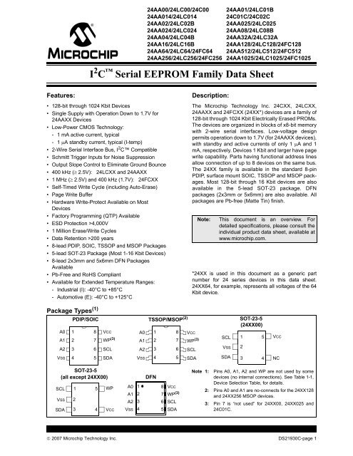
Package Types (1)<br />
PDIP/SOIC<br />
A0<br />
A1<br />
A2<br />
VSS<br />
1<br />
2<br />
3<br />
4<br />
8<br />
7<br />
6<br />
5<br />
VCC<br />
WP (3)<br />
SCL<br />
SDA<br />
SOT-23-5<br />
(all except 24XX00)<br />
SCL<br />
VSS<br />
SDA<br />
1 5<br />
2<br />
3<br />
A0<br />
A1<br />
A2<br />
VSS<br />
24AA00/24LC00/24C00 24AA01/24LC01B<br />
24AA014/24LC014 24C01C/24C02C<br />
24AA02/24LC02B 24AA025/24LC025<br />
24AA024/24LC024 24AA08/24LC08B<br />
24AA04/24LC04B 24AA32A/24LC32A<br />
24AA16/24LC16B 24AA128/24LC128/24FC128<br />
24AA64/24LC64/24FC64 24AA512/24LC512/24FC512<br />
24AA256/24LC256/24FC256 24AA1025/24LC1025/24FC1025<br />
I 2 C <strong>Serial</strong> <strong>EEPROM</strong> <strong>Family</strong> <strong>Data</strong> <strong>Sheet</strong><br />
4<br />
WP<br />
VCC<br />
A0<br />
A1<br />
A2<br />
VSS<br />
TSSOP/MSOP (2)<br />
1<br />
2<br />
3<br />
4<br />
DFN<br />
8<br />
7<br />
6<br />
5<br />
WP (3)<br />
1 8 VCC<br />
2 7<br />
3 6 SCL<br />
4 5 SDA<br />
Description:<br />
The <strong>Microchip</strong> Technology Inc. 24CXX, 24LCXX,<br />
24AAXX and 24FCXX (24XX*) devices are a family of<br />
128-bit through 1024 Kbit Electrically Erased PROMs.<br />
The devices are organized in blocks of x8-bit memory<br />
with 2-wire serial interfaces. Low-voltage design<br />
permits operation down to 1.7V (for 24AAXX devices),<br />
with standby and active currents of only 1 μA and 1<br />
mA, respectively. Devices 1 Kbit and larger have page<br />
write capability. Parts having functional address lines<br />
allow connection of up to 8 devices on the same bus.<br />
The 24XX family is available in the standard 8-pin<br />
PDIP, surface mount SOIC, TSSOP and MSOP packages.<br />
Most 128-bit through 16 Kbit devices are also<br />
available in the 5-lead SOT-23 package. DFN<br />
packages (2x3mm or 5x6mm) are also available. All<br />
packages are Pb-free (Matte Tin) finish.<br />
Note: This document is an overview. For<br />
detailed specifications, please consult the<br />
individual product data sheet, available at<br />
www.microchip.com.<br />
*24XX is used in this document as a generic part<br />
number for 24 series devices in this data sheet.<br />
24XX64, for example, represents all voltages of the 64<br />
Kbit device.<br />
© 2007 <strong>Microchip</strong> Technology Inc. DS21930C-page 1<br />
VCC<br />
WP (3)<br />
SCL<br />
SDA<br />
SCL<br />
VSS<br />
SDA<br />
SOT-23-5<br />
(24XX00)<br />
1 5<br />
2<br />
3<br />
4<br />
VCC<br />
NC<br />
Note 1: Pins A0, A1, A2 and WP are not used by some<br />
devices (no internal connections). See Table 1-1,<br />
Device Selection Table, for details.<br />
2: Pins A0 and A1 are no-connects for the 24XX128<br />
and 24XX256 MSOP devices.<br />
3: Pin 7 is “not used” for 24XX00, 24XX025 and<br />
24C01C.
24AAXX/24LCXX/24FCXX<br />
TABLE 1-1: DEVICE SELECTION TABLE<br />
Part Number<br />
VCC<br />
Range<br />
Max. Clock<br />
Frequency<br />
Page<br />
Size<br />
Write-<br />
Protect<br />
Array<br />
Functional<br />
Address<br />
Pins<br />
Temp.<br />
Range<br />
Packages (5)<br />
128-bit devices<br />
24AA00 1.7-5.5V 400 kHz (1)<br />
I P, SN, ST, OT, MC<br />
24LC00 2.5-5.5V 400 kHz — None None<br />
(1) I<br />
24C00 4.5-5.5V 400 kHz I, E<br />
1 Kb devices<br />
24AA01 1.7-5.5V 400 kHz (2)<br />
24LC01B 2.5-5.5V 400 kHz<br />
8 bytes Entire Array None<br />
I<br />
I, E<br />
P, SN, ST, MS, OT, MC<br />
24AA014 1.7-5.5V 400 kHz (2)<br />
24LC014 2.5-5.5V 400 kHz<br />
16 bytes Entire Array A0, A1, A2<br />
I<br />
I<br />
P, SN, ST, MS, MC<br />
24AA01H (6)<br />
1.7-5.5v 400 kHz (1)<br />
16 bytes Upper Half A0, A1, A2 I P, SN, ST, MS, OT, MC<br />
24LC01H (6)<br />
2.5-5.5v 400 kHz (1)<br />
16 bytes Upper Half A0, A1, A2 I, E P, SN, ST, MS, OT, MC<br />
24C01C<br />
2 Kb devices<br />
4.5V-5.5V 400 kHz 16 bytes None A0, A1, A2 I, E P, SN, ST, MC<br />
24AA02 1.7-5.5V 400 kHz (2)<br />
24LC02B 2.5-5.5V 400 kHz<br />
8 bytes Entire Array None<br />
I<br />
I, E<br />
P, SN, ST, MS, OT, MC<br />
24AA024 1.7-5.5V 400 kHz (2)<br />
24LC024 2.5-5.5V 400 kHz<br />
16 bytes Entire Array A0, A1, A2<br />
I<br />
I<br />
P, SN, ST, MS, MC<br />
24AA025 1.7-5.5V 400 kHz (2)<br />
24LC025 2.5-5.5V 400 kHz<br />
16 bytes None A0, A1, A2<br />
I<br />
I<br />
P, SN, ST,MS, MC<br />
24AA02H (6)<br />
1.7-5.5v 400 kHz (1)<br />
16 bytes Upper Half A0, A1, A2 I P, SN, ST, MS, OT, MC<br />
24LC02H (6)<br />
2.5-5.5v 400 kHz (1)<br />
16 bytes Upper Half A0, A1, A2 I, E P, SN, ST, MS, OT, MC<br />
24C02C 4.5-5.5V 400 kHz<br />
16 bytes Upper Half<br />
of Array<br />
A0, A1, A2 I, E P, SN, ST, MC<br />
4 Kb devices<br />
24AA04 1.7-5.5V 400 kHz (2)<br />
16 bytes Entire Array None I P, SN, ST, MS, OT, MC<br />
24LC04B<br />
8 Kb devices<br />
2.5-5.5V 400 kHz I, E<br />
24AA08 1.7-5.5V 400 kHz (2)<br />
24LC08B<br />
16 Kb devices<br />
2.5-5.5V 400 kHz<br />
16 bytes Entire Array None<br />
I<br />
I, E<br />
P, SN, ST, MS, OT, MC<br />
24AA16 1.7-5.5V 400 kHz (2)<br />
24LC16B<br />
32 Kb devices<br />
2.5-5.5V 400 kHz<br />
16 bytes Entire Array None<br />
I<br />
I, E<br />
P, SN, ST, MS, OT, MC<br />
24AA32A 1.7-5.5V 400 kHz (2)<br />
24LC32A 2.5-5.5V 400 kHz<br />
32 bytes Entire Array A0, A1, A2<br />
I<br />
I, E<br />
P, SN, SM, ST, MS, MC<br />
Note 1: 100 kHz for VCC
TABLE 1-1: DEVICE SELECTION TABLE (CONTINUED)<br />
Part Number<br />
VCC<br />
Range<br />
Max. Clock<br />
Frequency<br />
Page<br />
Size<br />
24AAXX/24LCXX/24FCXX<br />
Write-<br />
Protect<br />
Array<br />
Functional<br />
Address<br />
Pins<br />
Temp.<br />
Range<br />
Packages (5)<br />
64 Kb devices<br />
24AA64 1.7-5.5V 400 kHz (2)<br />
I P, SN, SM, ST, MS, MC<br />
24LC64 2.5-5.5V 400 kHz 32 bytes Entire Array A0, A1, A2 I, E<br />
24FC64 1.7-5.5V 1 MHz (3)<br />
128 Kb devices<br />
I<br />
24AA128 1.7-5.5V 400 kHz (2)<br />
64 bytes Entire Array<br />
A0, A1,<br />
A2 (4)<br />
24LC128<br />
24FC128<br />
2.5-5.5V<br />
1.7-5.5V<br />
400 kHz<br />
1 MHz<br />
I<br />
I, E<br />
P, SN, SM, ST, MS, MF<br />
(3)<br />
256 Kb devices<br />
I<br />
24AA256 1.7-5.5V 400 kHz (2)<br />
64 bytes Entire Array<br />
A0, A1,<br />
A2 (4)<br />
24LC256<br />
24FC256<br />
2.5-5.5V<br />
1.7-5.5V<br />
400 kHz<br />
1 MHz<br />
I<br />
I, E<br />
P, SN, SM, ST, MS, MF<br />
(3)<br />
512 Kb devices<br />
I<br />
24AA512 1.7-5.5V 400 kHz (2)<br />
24LC512<br />
24FC512<br />
2.5-5.5V<br />
1.7-5.5V<br />
400 kHz<br />
128<br />
bytes<br />
Entire Array A0, A1, A2<br />
I<br />
I, E<br />
P, SM, MF,<br />
(3) 1 MHz I<br />
1024 Kb devices<br />
24AA1025 1.7-5.5V 400 kHz (2)<br />
I P, SM<br />
24LC1025<br />
24FC1025<br />
2.5-5.5V<br />
1.7-5.5V<br />
400 kHz 128<br />
bytes<br />
Entire Array A0, A1 I, E<br />
(3) 1 MHz I<br />
Note 1: 100 kHz for VCC
24AAXX/24LCXX/24FCXX<br />
2.0 ELECTRICAL CHARACTERISTICS<br />
Absolute Maximum Ratings (†)<br />
VCC.............................................................................................................................................................................6.5V<br />
All inputs and outputs w.r.t. VSS ......................................................................................................... -0.6V to VCC +1.0V<br />
Storage temperature ...............................................................................................................................-65°C to +150°C<br />
Ambient temperature with power applied................................................................................................-40°C to +125°C<br />
ESD protection on all pins ......................................................................................................................................................≥ 4kV<br />
† NOTICE: Stresses above those listed under “Absolute Maximum Ratings” may cause permanent damage to<br />
the device. This is a stress rating only and functional operation of the device at those or any other conditions<br />
above those indicated in the operational listings of this specification is not implied. Exposure to maximum rating<br />
conditions for extended periods may affect device reliability.<br />
TABLE 2-1: DC CHARACTERISTICS<br />
Electrical Characteristics:<br />
DC CHARACTERISTICS<br />
Industrial (I): VCC = +1.7V to 5.5V TA = -40°C to +85°C<br />
Automotive (E): VCC = +2.5V to 5.5V TA = -40°C to 125°C<br />
Param.<br />
No.<br />
Sym. Characteristic Min. Max. Units Conditions<br />
D1 — A0, A1, A2, SCL, SDA and<br />
WP pins:<br />
— — — —<br />
D2 VIH High-level input voltage 0.7 VCC — V —<br />
D3 VIL Low-level input voltage — 0.3 VCC<br />
0.2 VCC<br />
D4 VHYS Hysteresis of Schmitt Trigger<br />
inputs (SDA, SCL pins)<br />
DS21930C-page 4 © 2007 <strong>Microchip</strong> Technology Inc.<br />
V<br />
V<br />
VCC ≥ 2.5V<br />
VCC < 2.5V<br />
0.05 VCC — V (Note 1)<br />
D5 VOL Low-level output voltage — 0.40 V IOL = 3.0 mA @ VCC = 2.5V<br />
D6 ILI Input leakage current — ±1 μA VIN = VSS or VCC<br />
D7 ILO Output leakage current — ±1 μA VOUT = VSS or VCC<br />
D8 CIN, Pin capacitance<br />
COUT (all inputs/outputs)<br />
D9 ICC Read Operating current — 500<br />
400<br />
1<br />
ICC Write — 3<br />
D10 ICCS Standby current —<br />
—<br />
— 10 pF VCC = 5.0V (Note 1)<br />
TA = 25°C, FCLK = 1 MHz<br />
5<br />
1<br />
5<br />
μA<br />
μA<br />
mA<br />
mA<br />
mA<br />
μA<br />
μA<br />
24XX1025<br />
24XX128, 256, 512:<br />
All except 24XX128, 256, 512,<br />
1025:<br />
(VCC = 5.5V, SCL = 400 kHz)<br />
All except 24XX512 and<br />
24XX1025<br />
24XX512 and 24XX1025<br />
(VCC = 5.5V)<br />
All except 24XX1025<br />
24XX1025<br />
— 50 μA 24C01C and 24C02C only<br />
(TA = -40°C to +85°C)<br />
— 5 μA All except 24XX1025<br />
(TA = -40°C to +125°C)<br />
SCL = SDA = VCC = 5.5V<br />
A0, A1, A2, WP = VSS or VCC<br />
Note 1: This parameter is periodically sampled and not 100% tested.
24AAXX/24LCXX/24FCXX<br />
TABLE 2-2: AC CHARACTERISTICS – ALL EXCEPT 24XX00, 24C01C<br />
AND 24C02C<br />
AC CHARACTERISTICS<br />
Param.<br />
No.<br />
1 FCLK Clock frequency —<br />
—<br />
—<br />
—<br />
2 THIGH Clock high time 4000<br />
600<br />
600<br />
500<br />
3 TLOW Clock low time 4700<br />
1300<br />
1300<br />
500<br />
Electrical Characteristics:<br />
Industrial (I): VCC = +1.7V to 5.5V TA = -40°C to +85°C<br />
Automotive (E): VCC = +2.5V to 5.5V TA = -40°C to 125°C<br />
Sym. Characteristic Min. Max. Units Conditions<br />
4 TR SDA and SCL rise time<br />
(Note 1)<br />
5 TF SDA and SCL fall time<br />
(Note 1)<br />
—<br />
—<br />
—<br />
—<br />
—<br />
6 THD:STA Start condition hold time 4000<br />
600<br />
600<br />
250<br />
7 TSU:STA Start condition setup time 4700<br />
600<br />
600<br />
250<br />
100<br />
400<br />
400<br />
1000<br />
kHz 1.7V ≤ VCC < 2.5V<br />
2.5V ≤ VCC ≤ 5.5V<br />
1.7V ≤ VCC < 2.5V 24FCXXX<br />
2.5V ≤ VCC ≤ 5.5V 24FCXXX<br />
© 2007 <strong>Microchip</strong> Technology Inc. DS21930C-page 5<br />
—<br />
—<br />
—<br />
—<br />
—<br />
—<br />
—<br />
—<br />
1000<br />
300<br />
300<br />
300<br />
100<br />
8 THD:DAT <strong>Data</strong> input hold time 0 — ns (Note 2)<br />
9 TSU:DAT <strong>Data</strong> input setup time 250<br />
100<br />
100<br />
10 TSU:STO Stop condition setup time 4000<br />
600<br />
600<br />
250<br />
11 TSU:WP WP setup time<br />
(32K and above only)<br />
12 THD:WP WP hold time<br />
(32K and above only)<br />
4000<br />
600<br />
600<br />
4700<br />
1300<br />
1300<br />
—<br />
—<br />
—<br />
—<br />
—<br />
—<br />
—<br />
—<br />
—<br />
—<br />
—<br />
—<br />
—<br />
—<br />
—<br />
—<br />
—<br />
—<br />
—<br />
—<br />
—<br />
ns 1.7V ≤ VCC < 2.5V<br />
2.5V ≤ VCC ≤ 5.5V<br />
1.7V ≤ VCC < 2.5V 24FCXXX<br />
2.5V ≤ VCC ≤ 5.5V 24FCXXX<br />
ns 1.7V ≤ VCC < 2.5V<br />
2.5V ≤ VCC ≤ 5.5V<br />
1.7V ≤ VCC < 2.5V 24FCXXX<br />
2.5V ≤ VCC ≤ 5.5V 24FCXXX<br />
ns 1.7V ≤ VCC < 2.5V<br />
2.5V ≤ VCC ≤ 5.5V<br />
1.7V ≤ VCC ≤ 5.5V 24FCXXX<br />
ns All except 24FCXXX<br />
1.7V ≤ VCC ≤ 5.5V 24FCXXX<br />
ns 1.7V ≤ VCC < 2.5V<br />
2.5V ≤ VCC ≤ 5.5V<br />
1.7V ≤ VCC < 2.5V 24FCXXX<br />
2.5V ≤ VCC ≤ 5.5V 24FCXXX<br />
ns 1.7V ≤ VCC < 2.5V<br />
2.5V ≤ VCC ≤ 5.5V<br />
1.7V ≤ VCC < 2.5V 24FCXXX<br />
2.5V ≤ VCC ≤ 5.5V 24FCXXX<br />
ns 1.7V ≤ VCC < 2.5V<br />
2.5V ≤ VCC ≤ 5.5V<br />
1.7V ≤ VCC ≤ 5.5V 24FCXXX<br />
ns 1.7 V ≤ VCC < 2.5V<br />
2.5 V ≤ VCC ≤ 5.5V<br />
1.7V ≤ VCC < 2.5V 24FCXXX<br />
2.5 V ≤ VCC ≤ 5.5V 24FCXXX<br />
ns 1.7V ≤ VCC < 2.5V<br />
2.5V ≤ VCC ≤ 5.5V<br />
1.7V ≤ VCC ≤ 5.5V 24FCXXX<br />
ns 1.7V ≤ VCC < 2.5V<br />
2.5V ≤ VCC ≤ 5.5V<br />
1.7V ≤ VCC ≤ 5.5V 24FCXXX<br />
Note 1: Not 100% tested. CB = total capacitance of one bus line in pF.<br />
2: As a transmitter, the device must provide an internal minimum delay time to bridge the undefined region<br />
(minimum 300 ns) of the falling edge of SCL to avoid unintended generation of Start or Stop conditions.<br />
3: This parameter is not tested but ensured by characterization. For endurance estimates in a specific<br />
application, please consult the Total Endurance Model, which can be obtained from <strong>Microchip</strong>’s web site:<br />
www.microchip.com.<br />
4: 24FCXXX denotes the 24FC64, 24FC128, 24FC256, 24FC512 and 24FC1025 devices.
24AAXX/24LCXX/24FCXX<br />
TABLE 2-2: AC CHARACTERISTICS – ALL EXCEPT 24XX00, 24C01C<br />
AND 24C02C (CONTINUED)<br />
AC CHARACTERISTICS<br />
Param.<br />
No.<br />
13 TAA Output valid from clock<br />
(Note 2)<br />
14 TBUF Bus free time: Time the bus<br />
must be free before a new<br />
transmission can start<br />
15 TOF Output fall time from VIH<br />
minimum to VIL maximum<br />
CB ≤ 100 pF<br />
16 TSP Input filter spike suppression<br />
(SDA and SCL pins)<br />
17 TWC Write cycle time (byte or<br />
page)<br />
Electrical Characteristics:<br />
Industrial (I): VCC = +1.7V to 5.5V TA = -40°C to +85°C<br />
Automotive (E): VCC = +2.5V to 5.5V TA = -40°C to 125°C<br />
Sym. Characteristic Min. Max. Units Conditions<br />
—<br />
—<br />
—<br />
—<br />
4700<br />
1300<br />
1300<br />
500<br />
DS21930C-page 6 © 2007 <strong>Microchip</strong> Technology Inc.<br />
3500<br />
900<br />
900<br />
400<br />
—<br />
—<br />
—<br />
—<br />
10 + 0.1CB 250<br />
250<br />
ns 1.7V ≤ VCC < 2.5V<br />
2.5V ≤ VCC ≤ 5.5V<br />
1.7V ≤ VCC < 2.5V 24FCXXX<br />
2.5V ≤ VCC ≤ 5.5V 24FCXXX<br />
ns 1.7V ≤ VCC < 2.5V<br />
2.5V ≤ VCC ≤ 5.5V<br />
1.7V ≤ VCC < 2.5V 24FCXXX<br />
2.5V ≤ VCC ≤ 5.5V 24FCXXX<br />
ns All except 24FCXXX (Note 1)<br />
24FCXXX (Note 1)<br />
— 50 ns All except 24FCXXX (Note 1)<br />
— 5 ms<br />
18 — Endurance 1,000,000 — cycles 25°C (Note 3)<br />
Note 1: Not 100% tested. CB = total capacitance of one bus line in pF.<br />
2: As a transmitter, the device must provide an internal minimum delay time to bridge the undefined region<br />
(minimum 300 ns) of the falling edge of SCL to avoid unintended generation of Start or Stop conditions.<br />
3: This parameter is not tested but ensured by characterization. For endurance estimates in a specific<br />
application, please consult the Total Endurance Model, which can be obtained from <strong>Microchip</strong>’s web site:<br />
www.microchip.com.<br />
4: 24FCXXX denotes the 24FC64, 24FC128, 24FC256, 24FC512 and 24FC1025 devices.
24AAXX/24LCXX/24FCXX<br />
TABLE 2-3: AC CHARACTERISTICS – 24XX00, 24C01C AND 24C02C<br />
All Parameters apply across all<br />
recommended operating ranges<br />
unless otherwise noted<br />
Industrial (I): TA = -40°C to +85°C, VCC = 1.7V to 5.5V<br />
Automotive (E): TA = -40°C to +125°C, VCC = 4.5V to 5.5V<br />
Parameter Symbol Min. Max. Units Conditions<br />
Clock frequency FCLK —<br />
—<br />
—<br />
Clock high time THIGH 4000<br />
4000<br />
600<br />
Clock low time TLOW 4700<br />
4700<br />
1300<br />
SDA and SCL rise time<br />
(Note 1)<br />
TR —<br />
—<br />
—<br />
© 2007 <strong>Microchip</strong> Technology Inc. DS21930C-page 7<br />
100<br />
100<br />
400<br />
—<br />
—<br />
—<br />
—<br />
—<br />
—<br />
1000<br />
1000<br />
300<br />
SDA and SCL fall time TF — 300 ns (Note 1)<br />
Start condition hold time THD:STA 4000<br />
4000<br />
600<br />
Start condition setup time TSU:STA 4700<br />
4700<br />
600<br />
<strong>Data</strong> input hold time THD:DAT 0 — ns (Note 2)<br />
<strong>Data</strong> input setup time TSU:DAT 250<br />
250<br />
100<br />
Stop condition setup time TSU:STO 4000<br />
4000<br />
600<br />
Output valid from clock<br />
(Note 2)<br />
Bus free time: Time the bus must<br />
be free before a new transmission<br />
can start<br />
Output fall time from VIH<br />
minimum to VIL maximum<br />
Input filter spike suppression<br />
(SDA and SCL pins)<br />
TAA —<br />
—<br />
—<br />
TBUF 4700<br />
4700<br />
1300<br />
TOF 20+0.1<br />
CB<br />
—<br />
—<br />
—<br />
—<br />
—<br />
—<br />
—<br />
—<br />
—<br />
—<br />
—<br />
—<br />
3500<br />
3500<br />
900<br />
—<br />
—<br />
—<br />
kHz 4.5V ≤ Vcc ≤ 5.5V (E Temp range)<br />
1.7V ≤ Vcc ≤ 4.5V<br />
4.5V ≤ Vcc ≤ 5.5V<br />
ns 4.5V ≤ Vcc ≤ 5.5V (E Temp range)<br />
1.7V ≤ Vcc ≤ 4.5V<br />
4.5V ≤ Vcc ≤ 5.5V<br />
ns 4.5V ≤ Vcc ≤ 5.5V (E Temp range)<br />
1.7V ≤ Vcc ≤ 4.5V<br />
4.5V ≤ Vcc ≤ 5.5V<br />
ns 4.5V ≤ Vcc ≤ 5.5V (E Temp range)<br />
1.7V ≤ Vcc ≤ 4.5V<br />
4.5V ≤ Vcc ≤ 5.5V<br />
ns 4.5V ≤ Vcc ≤ 5.5V (E Temp range)<br />
1.7V ≤ Vcc ≤ 4.5V<br />
4.5V ≤ Vcc ≤ 5.5V<br />
ns 4.5V ≤ Vcc ≤ 5.5V (E Temp range)<br />
1.7V ≤ Vcc ≤ 4.5V<br />
4.5V ≤ Vcc ≤ 5.5V<br />
ns 4.5V ≤ Vcc ≤ 5.5V (E Temp range)<br />
1.7V ≤ Vcc ≤ 4.5V<br />
4.5V ≤ Vcc ≤ 5.5V<br />
ns 4.5V ≤ Vcc ≤ 5.5V (E Temp range)<br />
1.7V ≤ Vcc ≤ 4.5V<br />
4.5V ≤ Vcc ≤ 5.5V<br />
ns 4.5V ≤ Vcc ≤ 5.5V (E Temp range)<br />
1.7V ≤ Vcc ≤ 4.5V<br />
4.5V ≤ Vcc ≤ 5.5V<br />
ns 4.5V ≤ Vcc ≤ 5.5V (E Temp range)<br />
1.7V ≤ Vcc ≤ 4.5V<br />
4.5V ≤ Vcc ≤ 5.5V<br />
250 ns (Note 1), CB ≤ 100 pF<br />
TSP — 50 ns (Note 1)<br />
Write cycle time TWC — 4<br />
1.5<br />
ms 24XX00<br />
24C01C, 24C02C<br />
Endurance 1,000,000 — cycles (Note 3)<br />
Note 1: Not 100% tested. CB = total capacitance of one bus line in pF.<br />
2: As a transmitter, the device must provide an internal minimum delay time to bridge the undefined region<br />
(minimum 300 ns) of the falling edge of SCL to avoid unintended generation of Start or Stop conditions.<br />
3: This parameter is not tested but ensured by characterization. For endurance estimates in a specific<br />
application, please consult the Total Endurance Model which can be obtained from <strong>Microchip</strong>’s web site:<br />
www.microchip.com.
24AAXX/24LCXX/24FCXX<br />
FIGURE 2-1: EXAMPLE BUS TIMING DATA<br />
SCL<br />
SDA<br />
IN<br />
SDA<br />
OUT<br />
WP<br />
16<br />
7<br />
6<br />
5<br />
3<br />
2<br />
8 9<br />
13<br />
(protected)<br />
(unprotected)<br />
DS21930C-page 8 © 2007 <strong>Microchip</strong> Technology Inc.<br />
D4<br />
4<br />
10<br />
14<br />
11 12
3.0 PIN DESCRIPTIONS<br />
The descriptions of the pins are listed in Table 3-1.<br />
TABLE 3-1: PIN FUNCTION TABLE<br />
Pin Name<br />
8-Pin PDIP<br />
and SOIC<br />
8-Pin<br />
TSSOP and<br />
MSOP<br />
A0 1 1 (1)<br />
5-Pin SOT-23<br />
24XX00<br />
3.1 A0, A1, A2 Chip Address Inputs<br />
The A0, A1 and A2 pins are not used by the 24XX01<br />
through 24XX16 devices.<br />
The A0, A1 and A2 inputs are used by the 24C01C,<br />
24C02C, 24XX014, 24XX024, 24XX025 and the<br />
24XX32 through 24XX1025 for multiple device operations.<br />
The levels on these inputs are compared with the<br />
corresponding bits in the slave address. The chip is<br />
selected if the compare is true.<br />
For the 24XX128 and 24XX256 in the MSOP package<br />
only, pins A0 and A1 are not connected.<br />
Up to eight devices (two for the 24XX128 and<br />
24XX256 MSOP package) may be connected to the<br />
same bus by using different Chip Select bit<br />
combinations.<br />
In most applications, the chip address inputs A0, A1<br />
and A2 are hard-wired to logic ‘0’ or logic ‘1’. For<br />
applications in which these pins are controlled by a<br />
microcontroller or other programmable device, the chip<br />
address pins must be driven to logic ‘0’ or logic ‘1’<br />
before normal device operation can proceed.<br />
24AAXX/24LCXX/24FCXX<br />
5-Pin SOT-23<br />
All except<br />
24XX00<br />
8-Pin<br />
5x6 DFN and<br />
2x3 DFN<br />
3.2 <strong>Serial</strong> <strong>Data</strong> (SDA)<br />
This is a bidirectional pin used to transfer addresses<br />
and data into and out of the device. It is an open drain<br />
terminal. Therefore, the SDA bus requires a pull-up<br />
resistor to VCC (typical 10 kΩ for 100 kHz, 2 kΩ for<br />
400 kHz and 1 MHz).<br />
For normal data transfer, SDA is allowed to change<br />
only during SCL low. Changes during SCL high are<br />
reserved for indicating the Start and Stop conditions.<br />
3.3 <strong>Serial</strong> Clock (SCL)<br />
This input is used to synchronize the data transfer to<br />
and from the device.<br />
3.4 Write-Protect (WP)<br />
This pin must be connected to either VSS or VCC. If tied<br />
to VSS, write operations are enabled. If tied to VCC,<br />
write operations are inhibited but read operations are<br />
not affected. See Table 1-1 for the write-protect<br />
scheme of each device.<br />
3.5 Power Supply (VCC)<br />
Function<br />
— — 1 User configurable Chip Select (3)(4)<br />
A1 2 2 (1) — — 2 User configurable Chip Select (3)(4)<br />
A2 3 3 — — 3 User configurable Chip Select (3)(4)<br />
VSS 4 4 2 2 4 Ground<br />
SDA 5 5 3 3 5 <strong>Serial</strong> <strong>Data</strong><br />
SCL 6 6 1 1 6 <strong>Serial</strong> Clock<br />
(NC) — — 4 — — Not Connected<br />
WP 7 (2)<br />
7 (2)<br />
— 5 7 Write-Protect Input<br />
VCC 8 8 5 4 8 Power Supply<br />
Note 1: Pins 1 and 2 are not connected for the 24XX128 and 24XX256 MSOP packages.<br />
2: Pin 7 is not used for 24XX00, 24XX025 and 24C01C.<br />
3: Pins A0, A1 and A2 are not used by some devices (no internal connections). See Table 1-1 for details.<br />
4: Pin A2 should be tied to a Logic High in the 24XX1025 for proper operation.<br />
Note: In the 24XX1025, the A2 pin is not configurable,<br />
it must be tied to VCC in order for<br />
this device to operate properly.<br />
A VCC threshold detect circuit is employed which<br />
disables the internal erase/write logic if VCC is below<br />
1.5V at nominal conditions. For the 24C00, 24C01C<br />
and 24C02C devices, the erase/write logic is disabled<br />
below 3.8V at nominal conditions.<br />
© 2007 <strong>Microchip</strong> Technology Inc. DS21930C-page 9
24AAXX/24LCXX/24FCXX<br />
4.0 FUNCTIONAL DESCRIPTION<br />
Each 24XX device supports a bidirectional, 2-wire bus<br />
and data transmission protocol. A device that sends<br />
data onto the bus is defined as a transmitter, while a<br />
device receiving data is defined as a receiver. The bus<br />
has to be controlled by a master device which generates<br />
the <strong>Serial</strong> Clock (SCL), controls the bus access<br />
and generates the Start and Stop conditions, while the<br />
24XX works as slave. Both master and slave can<br />
operate as transmitter or receiver, but the master<br />
device determines which mode is activated.<br />
Block Diagram<br />
A0*A1*A2* WP*<br />
I/O<br />
Control<br />
Logic<br />
I/O<br />
SDA<br />
VCC<br />
VSS<br />
SCL<br />
Memory<br />
Control<br />
Logic<br />
XDEC<br />
HV Generator<br />
<strong>EEPROM</strong><br />
Array<br />
Page Latches*<br />
YDEC<br />
Sense Amp.<br />
R/W Control<br />
* A0, A1, A2, WP and page latches are not used by some<br />
devices.<br />
See Table 1-1, Device Selection Table, for details.<br />
DS21930C-page 10 © 2007 <strong>Microchip</strong> Technology Inc.
5.0 BUS CHARACTERISTICS<br />
The following bus protocol has been defined:<br />
• <strong>Data</strong> transfer may be initiated only when the bus<br />
is not busy.<br />
• During data transfer, the data line must remain<br />
stable whenever the clock line is high. Changes in<br />
the data line while the clock line is high will be<br />
interpreted as a Start or Stop condition.<br />
Accordingly, the following bus conditions have been<br />
defined (Figure 5-1).<br />
5.1 Bus Not Busy (A)<br />
Both data and clock lines remain high.<br />
5.2 Start <strong>Data</strong> Transfer (B)<br />
A high-to-low transition of the SDA line while the clock<br />
(SCL) is high determines a Start condition. All<br />
commands must be preceded by a Start condition.<br />
5.3 Stop <strong>Data</strong> Transfer (C)<br />
A low-to-high transition of the SDA line while the clock<br />
(SCL) is high determines a Stop condition. All<br />
operations must be ended with a Stop condition.<br />
5.4 <strong>Data</strong> Valid (D)<br />
The state of the data line represents valid data when,<br />
after a Start condition, the data line is stable for the<br />
duration of the high period of the clock signal.<br />
The data on the line must be changed during the low<br />
period of the clock signal. There is one clock pulse per<br />
bit of data.<br />
Each data transfer is initiated with a Start condition and<br />
terminated with a Stop condition. The number of data<br />
bytes transferred between Start and Stop conditions is<br />
determined by the master device.<br />
24AAXX/24LCXX/24FCXX<br />
© 2007 <strong>Microchip</strong> Technology Inc. DS21930C-page 11
24AAXX/24LCXX/24FCXX<br />
5.5 Acknowledge<br />
Each receiving device, when addressed, is obliged to<br />
generate an acknowledge after the reception of each<br />
byte. The master device must generate an extra clock<br />
pulse which is associated with this Acknowledge bit.<br />
Note: During a write cycle, the 24XX will not<br />
acknowledge commands.<br />
FIGURE 5-1: DATA TRANSFER SEQUENCE ON THE SERIAL BUS<br />
SCL<br />
SDA<br />
FIGURE 5-2: ACKNOWLEDGE TIMING<br />
The device that acknowledges has to pull down the<br />
SDA line during the acknowledge clock pulse in such a<br />
way that the SDA line is stable low during the high<br />
period of the acknowledge related clock pulse. Of<br />
course, setup and hold times must be taken into<br />
account. During reads, a master must signal an end-ofdata<br />
to the slave by not generating an Acknowledge bit<br />
on the last byte that has been clocked out of the slave.<br />
In this case, the slave (24XX) will leave the data line<br />
high to enable the master to generate the Stop<br />
condition (Figure 5-2).<br />
(A) (B) (D) (D) (C) (A)<br />
Start<br />
Condition<br />
Address or<br />
Acknowledge<br />
Valid<br />
<strong>Data</strong><br />
Allowed<br />
to Change<br />
SCL 1 2 3 4 5 6 7 8 9 1 2 3<br />
SDA<br />
<strong>Data</strong> from transmitter<br />
Transmitter must release the SDA line at this point,<br />
allowing the Receiver to pull the SDA line low to<br />
acknowledge the previous eight bits of data.<br />
Acknowledge<br />
bit<br />
<strong>Data</strong> from transmitter<br />
Stop<br />
Condition<br />
Receiver must release the SDA line<br />
at this point so the Transmitter can<br />
continue sending data.<br />
DS21930C-page 12 © 2007 <strong>Microchip</strong> Technology Inc.
5.6 Device Addressing For Devices<br />
Without Functional Address Pins<br />
A control byte is the first byte received following the<br />
Start condition from the master device (Figure 5-3).<br />
The control byte begins with a four-bit control code. For<br />
the 24XX, this is set as ‘1010’ binary for read and write<br />
operations. The next three bits of the control byte are<br />
the block-select bits (B2, B1, B0). They are used by the<br />
master device to select which of the 256-word blocks of<br />
memory are to be accessed. These bits are in effect the<br />
three Most Significant bits of the word address. Note<br />
that B2, B1 and B0 are “don’t care” for the 24XX00, the<br />
24XX01 and 24XX02. B2 and B1 are “don’t care” for<br />
the 24XX04. B2 is “don’t care” for the 24XX08.<br />
24AAXX/24LCXX/24FCXX<br />
FIGURE 5-3: CONTROL AND ADDRESS BYTE ASSIGNMENTS FOR<br />
DEVICES WITHOUT ADDRESS PINS<br />
24XX00<br />
24XX01<br />
24XX02<br />
24XX04<br />
24XX08<br />
24XX016<br />
Start bit<br />
x = “don’t care” bit<br />
S 1 0 1 0 x x x R/W ACK<br />
S 1 0 1 0 x x x R/W ACK<br />
S 1 0 1 0 x x x R/W ACK<br />
S 1 0 1 0 x x B0 R/W ACK<br />
S 1 0 1 0 x B1 B0 R/W ACK<br />
S 1 0 1 0 B2 B1 B0 R/W ACK<br />
Control Code<br />
Control Byte<br />
Block Select bits<br />
The last bit of the control byte defines the operation to<br />
be performed. When set to ‘1’, a read operation is<br />
selected. When set to ‘0’ a write operation is selected.<br />
Following the Start condition, the 24XX monitors the<br />
SDA bus. Upon receiving a ‘1010’ code, the block<br />
select bits and the R/W bit, the slave device outputs an<br />
Acknowledge signal on the SDA line. The address byte<br />
follows the acknowledge.<br />
Acknowledge<br />
bit<br />
Read/Write bit (Read = 1, Write = 0)<br />
Address Byte<br />
x x x x A3 . . A0<br />
x A6 . . . . . A0<br />
A7 . . . . . . A0<br />
A7 . . . . . . A0<br />
A7 . . . . . . A0<br />
A7 . . . . . . A0<br />
© 2007 <strong>Microchip</strong> Technology Inc. DS21930C-page 13
24AAXX/24LCXX/24FCXX<br />
5.7 Device Addressing For Devices<br />
With Functional Address Pins<br />
A control byte is the first byte received following the<br />
Start condition from the master device (Figure 5-4).<br />
The control byte begins with a 4-bit control code. For<br />
the 24XX, this is set as ‘1010’ binary for read and write<br />
operations. The next three bits of the control byte are<br />
the Chip Select bits (A2, A1, A0). The Chip Select bits<br />
allow the use of up to eight 24XX devices on the same<br />
bus and are used to select which device is accessed.<br />
The Chip Select bits in the control byte must correspond<br />
to the logic levels on the corresponding A2, A1<br />
and A0 pins for the device to respond. These bits are,<br />
in effect, the three Most Significant bits of the word<br />
address.<br />
For 24XX128 and 24XX256 in the MSOP package, the<br />
A0 and A1 pins are not connected. During device<br />
addressing, the A0 and A1 Chip Select bits (Figure 5-4)<br />
should be set to ‘0’. Only two 24XX128 or 24XX256<br />
MSOP packages can be connected to the same bus.<br />
The last bit of the control byte defines the operation to<br />
be performed. When set to a ‘1’, a read operation is<br />
selected. When set to a ‘0’, a write operation is<br />
selected.<br />
FIGURE 5-4: CONTROL AND ADDRESS BYTE ASSIGNMENTS FOR<br />
DEVICES WITH ADDRESS PINS<br />
24C01C<br />
24C02C<br />
24XX024/025<br />
Start bit<br />
Control Code<br />
Chip Select bits*<br />
Control Byte<br />
S 1 0 1 0 A2 A1 A0 R/W ACK<br />
S 1 0 1 0 A2 A1 A0 R/W ACK<br />
S 1 0 1 0 A2 A1 A0 R/W ACK<br />
Control Byte<br />
24XX32 S 1 0 1 0 A2 A1 A0 R/W ACK<br />
24XX64 S 1 0 1 0 A2 A1 A0 R/W ACK<br />
24XX128 S 1 0 1 0 A2 A1 A0 R/W ACK<br />
24XX256 S 1 0 1 0 A2 A1 A0 R/W ACK<br />
24XX512 S 1 0 1 0 A2 A1 A0 R/W ACK<br />
24XX1025<br />
S 1 0 1 0 B0 A1 A0 R/W ACK<br />
Read/Write bit<br />
(Read = 1, Write = 0)<br />
Acknowledge<br />
bit<br />
x = “don’t care” bit<br />
* Chip Select bits A1 and A0 must be set to ‘0’ for 24XX128/256 devices in the MSOP package.<br />
For higher density devices (24XX32 through<br />
24XX1025), the next two bytes received define the<br />
address of the first data byte. Depending on the product<br />
density, not all bits in the address high byte are<br />
used. A15, A14, A13 and A12 are “don’t care” for<br />
24XX32. A15, A14 and A13 are “don’t care” for<br />
24XX64. A15 and A14 are “don’t care” for 24XX128.<br />
A15 is “don’t care” for 24XX256. All address bits are<br />
used for the 24XX512 and 24XX1025. The upper<br />
address bits are transferred first, followed by the Less<br />
Significant bits.<br />
Following the Start condition, the 24XX monitors the<br />
SDA bus. Upon receiving a ‘1010’ code, appropriate<br />
device select bits and the R/W bit, the slave device outputs<br />
an Acknowledge signal on the SDA line. The<br />
address byte(s) follow the acknowledge.<br />
The 24XX1025 has an internal address boundary<br />
limitation that is divided into two segments of 512 Kbits.<br />
Block select bit ‘B0’ is used to control access to each<br />
segment. Contiguous writes cannot be performed<br />
across this boundary.<br />
Address High Byte<br />
x x x x A11 A10 A9 A8<br />
x x x A12 A11 A10 A9 A8<br />
x x A13 A12 A11 A10 A9 A8<br />
x A14 A13 A12 A11 A10 A9 A8<br />
A15 A14 A13 A12 A11 A10 A9 A8<br />
A15 A14 A13 A12 A11 A10 A9 A8<br />
Address Byte<br />
x A6 . . . . . A0<br />
A7 . . . . . . A0<br />
A7 . . . . . . A0<br />
Address Low Byte<br />
A7 . . . . . . A0<br />
A7 . . . . . . A0<br />
A7 . . . . . . A0<br />
A7 . . . . . . A0<br />
A7 . . . . . . A0<br />
A7 . . . . . . A0<br />
DS21930C-page 14 © 2007 <strong>Microchip</strong> Technology Inc.
5.7.1 CONTIGUOUS ADDRESSING<br />
ACROSS MULTIPLE DEVICES<br />
Chip Select bits A2, A1 and A0 can be used to expand<br />
the contiguous address space by adding up to eight<br />
24XXs on the same bus. Software can use the three<br />
address bits of the control byte as the three Most<br />
Significant bits of the address byte. For example, in the<br />
24XX32 devices, software can use A0 of the control<br />
byte as address bit A12; A1 as address bit A13; and A2<br />
as address bit A14 (Table 5-1). It is not possible to<br />
sequentially read across device boundaries.<br />
TABLE 5-1: CONTROL BYTE ADDRESS BITS<br />
Maximum<br />
Devices<br />
24AAXX/24LCXX/24FCXX<br />
Maximum<br />
Contiguous<br />
Address Space<br />
Chip Select Bit<br />
A2<br />
Chip Select Bit<br />
A1<br />
Chip Select Bit<br />
A0<br />
1K (24C01C) 8 8 Kb A10 A9 A8<br />
1K (24XX014) 8 8 Kb A10 A9 A8<br />
2K (24C02C) 8 16 Kb A10 A9 A8<br />
2K (24XX024/025) 8 16 Kb A10 A9 A8<br />
32K (24XX32) 8 256 Kb A14 A13 A12<br />
64K (24XX64) 8 512 Kb A15 A14 A13<br />
128K (24XX128) 8 (1)<br />
1 Mb A16* A15* A14<br />
256K (24XX256) 8 (1)<br />
2 Mb A17* A16* A15<br />
512K (24XX512) 8 4 Mb A18 A17 A16<br />
1024K (24XX1025) 4 (2)<br />
4 Mb B0 (3)<br />
A17 A16<br />
Note 1: Up to two 24XX128 or 24XX256 devices in the MSOP package can be added for up to 256 kb or 512 kb of<br />
address space, respectively. Bits A0 and A1 must be set to ‘0’.<br />
2: Using the block select bit ‘B0’, up to four 24XX1025 devices can be cascaded together.<br />
3: For proper operation of the 24XX1025 the A2 pin must be tied to a logic high. Software addressing uses<br />
B0 to select between upper and lower 512 Kbit segments of memory.<br />
© 2007 <strong>Microchip</strong> Technology Inc. DS21930C-page 15
24AAXX/24LCXX/24FCXX<br />
6.0 WRITE OPERATIONS<br />
6.1 Byte Write<br />
A byte write operation begins with a Start condition<br />
from the master followed by the four-bit control code<br />
(see Figure 6-1 and Figure 6-2). The next 3 bits are<br />
either the Block Address bits (for devices without<br />
address pins) or the Chip Select bits (for devices with<br />
address pins). Then the master transmitter clocks the<br />
R/W bit (which is a logic low) onto the bus. The slave<br />
then generates an Acknowledge bit during the ninth<br />
clock cycle.<br />
The next byte transmitted by the master is the address<br />
byte (for 128-bit to 16 Kbit devices) or the high-order<br />
address byte (for 32-1024 Kbit devices). For 32 through<br />
1024 Kbit devices, the high-order address byte is<br />
followed by the low-order address byte. In either case,<br />
each address byte is acknowledged by the 24XX and<br />
the address bits are latched into the internal address<br />
counter of the 24XX.<br />
FIGURE 6-1: BYTE WRITE: 128-BIT TO 16 KBIT DEVICES<br />
Bus Activity<br />
Master<br />
SDA Line<br />
Bus Activity<br />
FIGURE 6-2: BYTE WRITE: 32 TO 1024 KBIT DEVICES<br />
Bus Activity<br />
Master<br />
SDA Line<br />
Bus Activity<br />
S<br />
T<br />
A<br />
R<br />
T<br />
Control<br />
Byte<br />
For the 24XX00 devices, only the lower four address<br />
bits are used by the device. The upper four bits are<br />
“don’t cares.”<br />
After receiving the ACK from the 24XX acknowledging<br />
the final address byte, the master device transmits the<br />
data word to be written into the addressed memory<br />
location. The 24XX acknowledges again and the<br />
master generates a Stop condition, which initiates the<br />
internal write cycle.<br />
If an attempt is made to write to an array with the WP<br />
pin held high, the device will acknowledge the<br />
command, but no write cycle will occur, no data will be<br />
written, and the device will immediately accept a new<br />
command. After a byte Write command, the internal<br />
address counter will increment to the next address<br />
location. During a write cycle, the 24XX will not<br />
acknowledge commands.<br />
Address<br />
Byte<br />
S P<br />
S<br />
T<br />
A<br />
R<br />
T<br />
Control<br />
Byte<br />
A<br />
C<br />
K<br />
High Order<br />
Address Byte<br />
Low Order<br />
Address Byte<br />
DS21930C-page 16 © 2007 <strong>Microchip</strong> Technology Inc.<br />
A<br />
C<br />
K<br />
<strong>Data</strong><br />
Byte<br />
<strong>Data</strong><br />
Byte<br />
S P<br />
A<br />
C<br />
K<br />
A<br />
C<br />
K<br />
A<br />
C<br />
K<br />
A<br />
C<br />
K<br />
S<br />
T<br />
O<br />
P<br />
A<br />
C<br />
K<br />
S<br />
T<br />
O<br />
P
6.2 Page Write<br />
The write control byte, word address byte(s), and the<br />
first data byte are transmitted to the 24XX in much the<br />
same way as in a byte write (see Figure 6-3 and<br />
Figure 6-4). The exception is that instead of generating<br />
a Stop condition, the master transmits up to one page<br />
of bytes (1) , which is temporarily stored in the on-chip<br />
page buffer. This data is then written into memory once<br />
the master has transmitted a Stop condition. Upon<br />
receipt of each word, the internal address counter is<br />
incremented by one. If the master should transmit more<br />
than one page of data prior to generating the Stop condition,<br />
the address counter will roll over and the previously<br />
received data will be overwritten. As with the byte<br />
write operation, once the Stop condition is received, an<br />
internal write cycle begins. During the write cycle, the<br />
24XX will not acknowledge commands.<br />
Page writes can be any number of bytes within a page<br />
(up to the page size), starting at any address. Only the<br />
data bytes being addressed will be changed within the<br />
page.<br />
If an attempt is made to write to the array with the WP<br />
pin held high, the device will acknowledge the<br />
command, but no write cycle will occur, no data will be<br />
written and the device will immediately accept a new<br />
command.<br />
Note 1: See Device Selection Table 1-1 for the<br />
page size of each device.<br />
FIGURE 6-3: PAGE WRITE: 1 KB TO 16 KBIT DEVICES<br />
Bus Activity<br />
Master<br />
SDA Line<br />
Bus Activity<br />
FIGURE 6-4: PAGE WRITE: 32 TO 1024 KBIT DEVICES<br />
Bus Activity<br />
Master<br />
SDA Line<br />
Bus Activity<br />
S<br />
T<br />
A<br />
R<br />
T<br />
S<br />
T<br />
A<br />
R<br />
T<br />
S<br />
Control<br />
Byte<br />
Address<br />
Byte<br />
* See Table 1-1 for maximum number of data bytes in a page.<br />
24AAXX/24LCXX/24FCXX<br />
6.3 Write-Protection<br />
The WP pin allows the user to write-protect the array<br />
when the pin is tied to VCC. See Device Selection<br />
Table 1-1 for the write-protect scheme of each device.<br />
If tied to VSS, the write protection is disabled. Please<br />
refer to the product data sheet for complete details.<br />
Note: Page write operations are limited to<br />
writing bytes within a single physical<br />
page, regardless of the number of<br />
bytes actually being written. Physical<br />
page boundaries start at addresses<br />
that are integer multiples of the page<br />
buffer size (or ‘page size’) and end at<br />
addresses that are integer multiples of<br />
[page size – 1]. If a Page Write<br />
command attempts to write across a<br />
physical page boundary, the result is<br />
that the data wraps around to the<br />
beginning of the current page (overwriting<br />
data previously stored there),<br />
instead of being written to the next<br />
page, as might be expected. It is therefore<br />
necessary for the application software<br />
to prevent page write operations<br />
that would attempt to cross a page<br />
boundary.<br />
Initial<br />
Second<br />
Final<br />
<strong>Data</strong> Byte <strong>Data</strong> Byte <strong>Data</strong> Byte*<br />
S P<br />
Control<br />
Byte<br />
A<br />
C<br />
K<br />
A<br />
C<br />
K<br />
High Order<br />
Address Byte<br />
A<br />
C<br />
K<br />
A<br />
C<br />
K<br />
Low Order<br />
Address Byte<br />
© 2007 <strong>Microchip</strong> Technology Inc. DS21930C-page 17<br />
A<br />
C<br />
K<br />
A<br />
C<br />
K<br />
A<br />
C<br />
K<br />
Initial<br />
Final<br />
<strong>Data</strong> Byte <strong>Data</strong> Byte*<br />
A<br />
C<br />
K<br />
A<br />
C<br />
K<br />
A<br />
C<br />
K<br />
S<br />
T<br />
O<br />
P<br />
S<br />
T<br />
O<br />
P<br />
P
24AAXX/24LCXX/24FCXX<br />
7.0 ACKNOWLEDGE POLLING<br />
Since the device will not acknowledge commands<br />
during a write cycle, this can be used to determine<br />
when the cycle is complete (This feature can be used<br />
to maximize bus throughput). Once the Stop condition<br />
for a Write command has been issued from the master,<br />
the device initiates the internally timed write cycle. ACK<br />
polling can be initiated immediately. This involves the<br />
master sending a Start condition, followed by the control<br />
byte for a Write command (R/W = 0). If the device<br />
is still busy with the write cycle, then no ACK will be<br />
returned. If no ACK is returned, the Start bit and control<br />
byte must be re-sent. If the cycle is complete, then the<br />
device will return the ACK and the master can then proceed<br />
with the next Read or Write command. See<br />
Figure 7-1 for flow diagram.<br />
FIGURE 7-1: ACKNOWLEDGE<br />
POLLING FLOW<br />
Send<br />
Write Command<br />
Send Stop<br />
Condition to<br />
Initiate Write Cycle<br />
Send Start<br />
Send Control Byte<br />
with R/W = 0<br />
Did Device<br />
Acknowledge<br />
(ACK = 0)?<br />
Next<br />
Operation<br />
DS21930C-page 18 © 2007 <strong>Microchip</strong> Technology Inc.<br />
Yes<br />
No
8.0 READ OPERATION<br />
Read operations are initiated in much the same way as<br />
write operations with the exception that the R/W bit of<br />
the control byte is set to ‘1’. There are three basic types<br />
of read operations: current address read, random read<br />
and sequential read.<br />
8.1 Current Address Read<br />
The 24XX contains an address counter that maintains<br />
the address of the last byte accessed, internally incremented<br />
by ‘1’. Therefore, if the previous read or write<br />
operation was to address ‘n’ (n is any legal address),<br />
the next current address read operation would access<br />
data from address n + 1.<br />
Upon receipt of the control byte with R/W bit set to ‘1’,<br />
the 24XX issues an acknowledge and transmits the<br />
8-bit data byte. The master will not acknowledge the<br />
transfer, but does generate a Stop condition and the<br />
24XX discontinues transmission (Figure 8-1).<br />
FIGURE 8-1: CURRENT ADDRESS<br />
READ<br />
Bus Activity<br />
Master<br />
SDA Line<br />
Bus Activity<br />
S<br />
T<br />
A<br />
R<br />
T<br />
S<br />
FIGURE 8-2: RANDOM READ: 128-BIT TO 16 KBIT DEVICES<br />
Bus Activity<br />
Master<br />
SDA Line<br />
Bus Activity<br />
Control<br />
Byte<br />
A<br />
C<br />
K<br />
<strong>Data</strong><br />
Byte<br />
FIGURE 8-3: RANDOM READ: 32 TO 1024 KBIT DEVICES<br />
Bus Activity<br />
Master<br />
SDA Line<br />
Bus Activity<br />
S<br />
T<br />
A<br />
R<br />
T<br />
S<br />
T<br />
A<br />
R<br />
T<br />
Control<br />
Byte<br />
N<br />
O<br />
A<br />
C<br />
K<br />
24AAXX/24LCXX/24FCXX<br />
S<br />
T<br />
O<br />
P<br />
P<br />
8.2 Random Read<br />
Random read operations allow the master to access<br />
any memory location in a random manner. To perform<br />
this type of read operation, the byte address must first<br />
be set. This is done by sending the byte address to the<br />
24XX as part of a write operation (R/W bit set to ‘0’).<br />
Once the byte address is sent, the master generates a<br />
Start condition following the acknowledge. This terminates<br />
the write operation, but not before the internal<br />
address counter is set. The master then issues the<br />
control byte again, but with the R/W bit set to a ‘1’. The<br />
24XX will then issue an acknowledge and transmit the<br />
8-bit data byte. The master will not acknowledge the<br />
transfer but does generate a Stop condition, which<br />
causes the 24XX to discontinue transmission<br />
(Figure 8-2 and Figure 8-3). After a random Read<br />
command, the internal address counter will increment<br />
to the next address location.<br />
S S<br />
P<br />
Control<br />
Byte<br />
A<br />
C<br />
K<br />
A<br />
C<br />
K<br />
Address<br />
Byte (n)<br />
High Order<br />
Address Byte<br />
A<br />
C<br />
K<br />
A<br />
C<br />
K<br />
S<br />
T<br />
A<br />
R<br />
T<br />
Control<br />
Byte<br />
Low Order<br />
Address Byte<br />
© 2007 <strong>Microchip</strong> Technology Inc. DS21930C-page 19<br />
A<br />
C<br />
K<br />
A<br />
C<br />
K<br />
<strong>Data</strong><br />
Byte<br />
Control<br />
Byte<br />
N<br />
O<br />
A<br />
C<br />
K<br />
A<br />
C<br />
K<br />
S<br />
T<br />
O<br />
P<br />
<strong>Data</strong><br />
Byte<br />
S S P<br />
S<br />
T<br />
A<br />
R<br />
T<br />
N<br />
O<br />
A<br />
C<br />
K<br />
S<br />
T<br />
O<br />
P
24AAXX/24LCXX/24FCXX<br />
8.3 Sequential Read<br />
Sequential reads are initiated in the same way as a<br />
random read except that after the 24XX transmits the<br />
first data byte, the master issues an acknowledge as<br />
opposed to the Stop condition used in a random read.<br />
This acknowledge directs the 24XX to transmit the next<br />
sequentially addressed data byte (Figure 8-4). Following<br />
the final byte transmitted to the master, the master<br />
will NOT generate an acknowledge but will generate a<br />
Stop condition. To provide sequential reads, the 24XX<br />
contains an internal Address Pointer which is incremented<br />
by one at the completion of each operation.<br />
This Address Pointer allows the entire memory contents<br />
to be serially read during one operation. If the last<br />
address byte in the array is acknowledged, the Address<br />
Pointer will roll over to address 0x00.<br />
FIGURE 8-4: SEQUENTIAL READ<br />
Bus Activity<br />
Master<br />
SDA Line<br />
Bus Activity<br />
Control Initial Second Third Final<br />
Byte <strong>Data</strong> Byte <strong>Data</strong> Byte <strong>Data</strong> Byte <strong>Data</strong> Byte<br />
A<br />
C<br />
K<br />
A<br />
C<br />
K<br />
DS21930C-page 20 © 2007 <strong>Microchip</strong> Technology Inc.<br />
A<br />
C<br />
K<br />
A<br />
C<br />
K<br />
N<br />
O<br />
A<br />
C<br />
K<br />
S<br />
T<br />
O<br />
P<br />
P
APPENDIX A: REVISION HISTORY<br />
Revision A<br />
Original release of document. Combined <strong>Serial</strong><br />
<strong>EEPROM</strong> 24XXX device data sheets.<br />
Revision B (02/2007)<br />
Change 1.8V to 1.7V; Removed 14-Lead TSSOP<br />
Package; Replaced Package Drawings; Revised<br />
Product ID Section. Updates throughout.<br />
Revision C (07/2007)<br />
Added 24AA1025/LC1025/FC1025 part; Updates<br />
throughout; Replaced Package Drawings (Rev. AP).<br />
24AAXX/24LCXX/24FCXX<br />
© 2007 <strong>Microchip</strong> Technology Inc. DS21930C-page 21
24AAXX/24LCXX/24FCXX<br />
9.0 PACKAGING INFORMATION<br />
9.1 Package Marking Information<br />
Device<br />
8-Lead PDIP<br />
XXXXXXXX<br />
XXXXXNNN<br />
YYWW<br />
Line 1<br />
Marking<br />
Device<br />
Example:<br />
24LC01B<br />
I/P e3<br />
1L7<br />
0528<br />
8-Lead PDIP Package Marking<br />
Line 1<br />
Marking<br />
Device<br />
Line 1<br />
Marking<br />
Device<br />
Line 1<br />
Marking<br />
24AA00 24AA00 24LC00 24LC00 24C00 24C00<br />
24AA01 24AA01 24LC01B 24LC01B<br />
24AA014 24AA014 24LC014 24LC014<br />
24C01C 24C01C<br />
24AA02 24AA02 24LC02B 24LC02B<br />
24AA024 24AA024 24LC024 24LC024<br />
24AA025 24AA025 24LC025 24LC025<br />
24C02C 24C02C<br />
24AA04 24AA04 24LC04B 24LC04B<br />
24AA08 24AA08 24LC08B 24LC08B<br />
24AA16 24AA16 24LC16B 24LC16B<br />
24AA32A 24AA32A 24LC32A 24LC32A<br />
24AA64 24AA64 24LC64 24LC64 24FC64 24FC64<br />
24AA128 24AA128 24LC128 24LC128 24FC128 24FC128<br />
24AA256 24AA256 24LC256 24LC256 24FC256 24FC256<br />
24AA512 24AA512 24LC512 24LC512 24FC512 24FC512<br />
24AA1025 24AA1025 24LC1025 24LC1025 24FC1025 24FC1025<br />
Legend: XX...X Part number or part number code<br />
Y Year code (last digit of calendar year)<br />
YY Year code (last 2 digits of calendar year)<br />
WW Week code (week of January 1 is week ‘01’)<br />
NNN Alphanumeric traceability code (2 characters for small packages)<br />
e3<br />
Pb-free JEDEC designator for Matte Tin (Sn) plated devices<br />
Note: For very small packages with no room for the Pb-free JEDEC designator<br />
e3,<br />
the marking will only appear on the outer carton or reel label.<br />
Note: In the event the full <strong>Microchip</strong> part number cannot be marked on one line, it will<br />
be carried over to the next line, thus limiting the number of available<br />
characters for customer-specific information.<br />
Note: Please visit www.microchip.com/Pbfree for the latest information on Pb-free conversion.<br />
DS21930C-page 22 © 2007 <strong>Microchip</strong> Technology Inc.
Device<br />
Line 1<br />
Marking<br />
8-Lead SOIC<br />
XXXXXXXX<br />
XXXXXYYWW<br />
NNN<br />
Device<br />
Note: T = Temperature range: I = Industrial, E = Extended<br />
24AAXX/24LCXX/24FCXX<br />
Example:<br />
24LC01BI<br />
SN e3<br />
0528<br />
1L7<br />
8-Lead SOIC Package Marking<br />
Line 1<br />
Marking<br />
Device<br />
Line 1<br />
Marking<br />
Device<br />
Line 1<br />
Marking<br />
24AA00 24AA00T 24LC00 24LC00T 24C00 24C00T<br />
24AA01 24AA01T 24LC01B 24LC01BT<br />
24AA014 24AA014T 24LC014 24LC014T<br />
24C01C 24C01CT<br />
24AA02 24AA02T 24LC02B 24LC02BT<br />
24AA024 24AA024T 24LC024 24LC024T<br />
24AA025 24AA025T 24LC025 24LC025T<br />
24C02C 24C02CT<br />
24AA04 24AA04T 24LC04B 24LC04BT<br />
24AA08 24AA08T 24LC08B 24LC08BT<br />
24AA16 24AA16T 24LC16B 24LC16BT<br />
24AA32A 24AA32AT 24LC32A 24LC32AT<br />
24AA64 24AA64T 24LC64 24LC64T 24FC64 24FC64T<br />
24AA128 24AA128T 24LC128 24LC128T 24FC128 24FC128T<br />
24AA256 24AA256T 24LC256 24LC256T 24FC256 24FC256T<br />
24AA512 24AA512T 24LC512 24LC512T 24FC512 24FC512T<br />
24AA1025 24AA1025 24LC1025 24LC1025 24FC1025 24FC1025<br />
Legend: XX...X Part number or part number code<br />
Y Year code (last digit of calendar year)<br />
YY Year code (last 2 digits of calendar year)<br />
WW Week code (week of January 1 is week ‘01’)<br />
NNN Alphanumeric traceability code (2 characters for small packages)<br />
e3<br />
Pb-free JEDEC designator for Matte Tin (Sn) plated devices<br />
Note: For very small packages with no room for the Pb-free JEDEC designator<br />
e3,<br />
the marking will only appear on the outer carton or reel label.<br />
Note: In the event the full <strong>Microchip</strong> part number cannot be marked on one line, it will<br />
be carried over to the next line, thus limiting the number of available<br />
characters for customer-specific information.<br />
Note: Please visit www.microchip.com/Pbfree for the latest information on Pb-free conversion.<br />
© 2007 <strong>Microchip</strong> Technology Inc. DS21930C-page 23
24AAXX/24LCXX/24FCXX<br />
8-Lead 2x3 DFN Example:<br />
Device<br />
XXX<br />
YWW<br />
NN<br />
Industrial<br />
Line 1<br />
Marking<br />
Device<br />
244<br />
506<br />
L7<br />
8-Lead 2x3mm DFN Package Marking<br />
Industrial<br />
Line 1<br />
Marking<br />
E-Temp<br />
Line 1<br />
Marking<br />
Device<br />
Industrial<br />
Line 1<br />
Marking<br />
E-Temp<br />
Line 1<br />
Marking<br />
24AA00 201 24LC00 204 205 24C00 207 208<br />
24AA01 211 24LC01B 214 215<br />
24AA014 2N1 24LC014 2N4 2N5<br />
24C01C 2N7 2N8<br />
24AA02 221 24LC02B 224 225<br />
24AA024 2P1 24LC024 2P4 2P5<br />
24AA025 2R1 24LC025 2R4 2R5<br />
24C02C 2P7 2P8<br />
24AA04 231 24LC04B 234 235<br />
24AA08 241 24LC08B 244 245<br />
24AA16 251 24LC16B 254 255<br />
24AA32A 261 24LC32A 264 265<br />
24AA64 271 24LC64 274 275 24FC64 27A 27B<br />
Legend: XX...X Part number or part number code<br />
Y Year code (last digit of calendar year)<br />
YY Year code (last 2 digits of calendar year)<br />
WW Week code (week of January 1 is week ‘01’)<br />
NNN Alphanumeric traceability code (2 characters for small packages)<br />
e3<br />
Pb-free JEDEC designator for Matte Tin (Sn) plated devices<br />
Note: For very small packages with no room for the Pb-free JEDEC designator<br />
e3,<br />
the marking will only appear on the outer carton or reel label.<br />
Note: In the event the full <strong>Microchip</strong> part number cannot be marked on one line, it will<br />
be carried over to the next line, thus limiting the number of available<br />
characters for customer-specific information.<br />
DS21930C-page 24 © 2007 <strong>Microchip</strong> Technology Inc.
Device<br />
8-Lead DFN Example:<br />
XXXXXXX<br />
T/XXXXX<br />
YYWW<br />
NNN<br />
Line 1<br />
Marking<br />
Note: Temperature range (T) listed on second line. I = Industrial, E = Extended<br />
24AAXX/24LCXX/24FCXX<br />
24AA128<br />
I/MF e3<br />
0528<br />
1L7<br />
8-Lead 5x6mm DFN Package Marking<br />
Device<br />
Line 1<br />
Marking<br />
Device<br />
Line 1<br />
Marking<br />
24AA128 24AA128 24LC128 24LC128 24FC128 24FC128<br />
24AA256 24AA256 24LC256 24LC256 24FC256 24FC256<br />
24AA512 24AA512 24LC512 24LC512 24FC512 24FC512<br />
Legend: XX...X Part number or part number code<br />
Y Year code (last digit of calendar year)<br />
YY Year code (last 2 digits of calendar year)<br />
WW Week code (week of January 1 is week ‘01’)<br />
NNN Alphanumeric traceability code (2 characters for small packages)<br />
e3<br />
Pb-free JEDEC designator for Matte Tin (Sn) plated devices<br />
Note: For very small packages with no room for the Pb-free JEDEC designator<br />
e3,<br />
the marking will only appear on the outer carton or reel label.<br />
Note: In the event the full <strong>Microchip</strong> part number cannot be marked on one line, it will<br />
be carried over to the next line, thus limiting the number of available<br />
characters for customer-specific information.<br />
© 2007 <strong>Microchip</strong> Technology Inc. DS21930C-page 25
24AAXX/24LCXX/24FCXX<br />
5-Lead SOT-23<br />
XXNN<br />
Device Comm.<br />
Marking<br />
Indust.<br />
Marking<br />
Device<br />
Example:<br />
5EL7<br />
5-Lead SOT-23 Package Marking<br />
Comm.<br />
Marking<br />
Indust.<br />
Marking<br />
E-Temp<br />
Marking<br />
Device Comm.<br />
Marking<br />
Indust.<br />
Marking<br />
E-Temp<br />
Marking<br />
24AA00 A0NN B0NN 24LC00 L0NN M0NN N0NN 24C00 C0NN D0NN E0NN<br />
24AA01 A1NN B1NN 24LC01B L1NN M1NN N1NN<br />
24AA02 A2NN B2NN 24LC02B L2NN M2NN N2NN<br />
24AA04 A3NN B3NN 24LC04B L3NN M3NN N3NN<br />
24AA08 A4NN B4NN 24LC08B L4NN M4NN N4NN<br />
24AA16 A5NN B5NN 24LC16B L5NN M5NN N5NN<br />
Legend: XX...X Part number or part number code<br />
Y Year code (last digit of calendar year)<br />
YY Year code (last 2 digits of calendar year)<br />
WW Week code (week of January 1 is week ‘01’)<br />
NNN Alphanumeric traceability code (2 characters for small packages)<br />
e3<br />
Pb-free JEDEC designator for Matte Tin (Sn) plated devices<br />
Note: For very small packages with no room for the Pb-free JEDEC designator<br />
e3,<br />
the marking will only appear on the outer carton or reel label.<br />
Note: In the event the full <strong>Microchip</strong> part number cannot be marked on one line, it will<br />
be carried over to the next line, thus limiting the number of available<br />
characters for customer-specific information.<br />
DS21930C-page 26 © 2007 <strong>Microchip</strong> Technology Inc.
8-Lead MSOP (150 mil) Example:<br />
Device<br />
XXXXXXT<br />
YWWNNN<br />
Line 1<br />
Marking<br />
Device<br />
4L8BI<br />
2281L7<br />
Note: T = Temperature range: I = Industrial, E = Extended<br />
24AAXX/24LCXX/24FCXX<br />
8-Lead MSOP Package Marking<br />
Line 1<br />
Marking<br />
Device<br />
Line 1<br />
Marking<br />
Device<br />
Line 1<br />
Marking<br />
24AA01 4A01T 24LC01B 4L1BT<br />
24AA014 4A14T 24LC014 4L14T<br />
24C01C 4C1CT<br />
24AA02 4A02T 24LC02B 4L2BT<br />
24AA024 4A24T 24LC024 4L24T<br />
24AA025 4A25T 24LC025 4L25T<br />
24C02C 4C2CT<br />
24AA04 4A04T 24LC04B 4L4BT<br />
24AA08 4A08T 24LC08B 4L8BT<br />
24AA16 4A16T 24LC16B 4L16T<br />
24AA32A 4A32AT 24LC32A 4L32AT<br />
24AA64 4A64T 24LC64 4L64T 24FC64 4F64T<br />
24AA128 4A128T 24LC128 4L128T 24FC128 4F128T<br />
24AA256 4A256T 24LC256 4L256T 24FC256 4F256T<br />
Legend: XX...X Part number or part number code<br />
Y Year code (last digit of calendar year)<br />
YY Year code (last 2 digits of calendar year)<br />
WW Week code (week of January 1 is week ‘01’)<br />
NNN Alphanumeric traceability code (2 characters for small packages)<br />
e3<br />
Pb-free JEDEC designator for Matte Tin (Sn) plated devices<br />
Note: For very small packages with no room for the Pb-free JEDEC designator<br />
e3,<br />
the marking will only appear on the outer carton or reel label.<br />
Note: In the event the full <strong>Microchip</strong> part number cannot be marked on one line, it will<br />
be carried over to the next line, thus limiting the number of available<br />
characters for customer-specific information.<br />
© 2007 <strong>Microchip</strong> Technology Inc. DS21930C-page 27
24AAXX/24LCXX/24FCXX<br />
8-Lead TSSOP<br />
Device<br />
XXXX<br />
TYWW<br />
NNN<br />
Line 1<br />
Marking<br />
Device<br />
Example:<br />
4L08<br />
I228<br />
1L7<br />
8-Lead TSSOP Package Marking<br />
Line 1<br />
Marking<br />
Note: T = Temperature range: I = Industrial, E = Extended<br />
Device<br />
Line 1<br />
Marking<br />
Device<br />
Line 1<br />
Marking<br />
24AA00 4A00 24LC00 4L00 24C00 4C00<br />
24AA01 4A01 24LC01B 4L1B<br />
24AA014 4A14 24LC014 4L14<br />
24C01C 4C1C<br />
24AA02 4A02 24LC02B 4L02<br />
24AA024 4A24 24LC024 4L24<br />
24AA025 4A25 24LC025 4L25<br />
24C02C 4C2C<br />
24AA04 4A04 24LC04B 4L04<br />
24AA08 4A08 24LC08B 4L08<br />
24AA16 4A16 24LC16B 4L16<br />
24AA32A 4AA 24LC32A 4LA<br />
24AA64 4AB 24LC64 4LB 24FC64 4FB<br />
24AA128 4AC 24LC128 4LC 24FC128 4FC<br />
24AA256 4AD 24LC256 4LD 24FC256 4FD<br />
Legend: XX...X Part number or part number code<br />
Y Year code (last digit of calendar year)<br />
YY Year code (last 2 digits of calendar year)<br />
WW Week code (week of January 1 is week ‘01’)<br />
NNN Alphanumeric traceability code (2 characters for small packages)<br />
e3<br />
Pb-free JEDEC designator for Matte Tin (Sn) plated devices<br />
Note: For very small packages with no room for the Pb-free JEDEC designator<br />
e3,<br />
the marking will only appear on the outer carton or reel label.<br />
Note: In the event the full <strong>Microchip</strong> part number cannot be marked on one line, it will<br />
be carried over to the next line, thus limiting the number of available<br />
characters for customer-specific information.<br />
DS21930C-page 28 © 2007 <strong>Microchip</strong> Technology Inc.
8-Lead Plastic Dual In-Line (P) – 300 mil Body [PDIP]<br />
24AAXX/24LCXX/24FCXX<br />
Note: For the most current package drawings, please see the <strong>Microchip</strong> Packaging Specification located at<br />
http://www.microchip.com/packaging<br />
NOTE 1<br />
A<br />
A1<br />
N<br />
b1<br />
b<br />
1 2 3<br />
D<br />
e<br />
Units INCHES<br />
Dimension Limits MIN NOM MAX<br />
Number of Pins N 8<br />
Pitch e .100 BSC<br />
Top to Seating Plane A – – .210<br />
Molded Package Thickness A2 .115 .130 .195<br />
Base to Seating Plane A1 .015 – –<br />
Shoulder to Shoulder Width E .290 .310 .325<br />
Molded Package Width E1 .240 .250 .280<br />
Overall Length D .348 .365 .400<br />
Tip to Seating Plane L .115 .130 .150<br />
Lead Thickness c .008 .010 .015<br />
Upper Lead Width b1 .040 .060 .070<br />
Lower Lead Width b .014 .018 .022<br />
Overall Row Spacing § eB – – .430<br />
Notes:<br />
1. Pin 1 visual index feature may vary, but must be located with the hatched area.<br />
2. § Significant Characteristic.<br />
3. Dimensions D and E1 do not include mold flash or protrusions. Mold flash or protrusions shall not exceed .010" per side.<br />
4. Dimensioning and tolerancing per ASME Y14.5M.<br />
BSC: Basic Dimension. Theoretically exact value shown without tolerances.<br />
E1<br />
L<br />
© 2007 <strong>Microchip</strong> Technology Inc. DS21930C-page 29<br />
A2<br />
E<br />
eB<br />
c<br />
<strong>Microchip</strong> Technology Drawing C04-018B
24AAXX/24LCXX/24FCXX<br />
8-Lead Plastic Small Outline (SN) – Narrow, 3.90 mm Body [SOIC]<br />
Note: For the most current package drawings, please see the <strong>Microchip</strong> Packaging Specification located at<br />
http://www.microchip.com/packaging<br />
NOTE 1<br />
A<br />
A1<br />
N<br />
D<br />
1 2 3<br />
b<br />
e<br />
E1<br />
A2<br />
E<br />
Units MILLIMETERS<br />
Dimension Limits MIN NOM MAX<br />
Number of Pins N 8<br />
Pitch e 1.27 BSC<br />
Overall Height A – – 1.75<br />
Molded Package Thickness A2 1.25 – –<br />
Standoff § A1 0.10 – 0.25<br />
Overall Width E 6.00 BSC<br />
Molded Package Width E1 3.90 BSC<br />
Overall Length D 4.90 BSC<br />
Chamfer (optional) h 0.25 – 0.50<br />
Foot Length L 0.40 – 1.27<br />
Footprint L1 1.04 REF<br />
Foot Angle φ 0° – 8°<br />
Lead Thickness c 0.17 – 0.25<br />
Lead Width b 0.31 – 0.51<br />
Mold Draft Angle Top α 5° – 15°<br />
Mold Draft Angle Bottom β 5° – 15°<br />
Notes:<br />
1. Pin 1 visual index feature may vary, but must be located within the hatched area.<br />
2. § Significant Characteristic.<br />
3. Dimensions D and E1 do not include mold flash or protrusions. Mold flash or protrusions shall not exceed 0.15 mm per side.<br />
4. Dimensioning and tolerancing per ASME Y14.5M.<br />
BSC: Basic Dimension. Theoretically exact value shown without tolerances.<br />
REF: Reference Dimension, usually without tolerance, for information purposes only.<br />
φ<br />
DS21930C-page 30 © 2007 <strong>Microchip</strong> Technology Inc.<br />
h<br />
L<br />
L1<br />
h<br />
α<br />
β<br />
c<br />
<strong>Microchip</strong> Technology Drawing C04-057B
24AAXX/24LCXX/24FCXX<br />
8-Lead Plastic Dual Flat, No Lead Package (MC) – 2x3x0.9 mm Body [DFN]<br />
Note: For the most current package drawings, please see the <strong>Microchip</strong> Packaging Specification located at<br />
http://www.microchip.com/packaging<br />
NOTE 1<br />
N<br />
1 2<br />
D<br />
TOP VIEW<br />
A3 A1<br />
Units MILLIMETERS<br />
Dimension Limits MIN NOM MAX<br />
Number of Pins N 8<br />
Pitch e 0.50 BSC<br />
Overall Height A 0.80 0.90 1.00<br />
Standoff A1 0.00 0.02 0.05<br />
Contact Thickness A3 0.20 REF<br />
Overall Length D 2.00 BSC<br />
Overall Width E 3.00 BSC<br />
Exposed Pad Length D2 1.30 – 1.75<br />
Exposed Pad Width E2 1.50 – 1.90<br />
Contact Width b 0.18 0.25 0.30<br />
Contact Length L 0.30 0.40 0.50<br />
Contact-to-Exposed Pad K 0.20 – –<br />
Notes:<br />
1. Pin 1 visual index feature may vary, but must be located within the hatched area.<br />
2. Package may have one or more exposed tie bars at ends.<br />
3. Package is saw singulated.<br />
4. Dimensioning and tolerancing per ASME Y14.5M.<br />
BSC: Basic Dimension. Theoretically exact value shown without tolerances.<br />
REF: Reference Dimension, usually without tolerance, for information purposes only.<br />
E<br />
A<br />
EXPOSED PAD<br />
NOTE 2<br />
2 1<br />
D2<br />
NOTE 1<br />
© 2007 <strong>Microchip</strong> Technology Inc. DS21930C-page 31<br />
L<br />
K<br />
b<br />
e<br />
BOTTOM VIEW<br />
N<br />
E2<br />
<strong>Microchip</strong> Technology Drawing C04-123B
24AAXX/24LCXX/24FCXX<br />
8-Lead Plastic Dual Flat, No Lead Package (MF) – 6x5 mm Body [DFN-S]<br />
Note: For the most current package drawings, please see the <strong>Microchip</strong> Packaging Specification located at<br />
http://www.microchip.com/packaging<br />
A3<br />
N<br />
NOTE 1 1 2<br />
D<br />
TOP VIEW<br />
A1<br />
E<br />
A<br />
NOTE 2<br />
EXPOSED PAD<br />
2 1<br />
D2<br />
Units MILLIMETERS<br />
Dimension Limits MIN NOM MAX<br />
Number of Pins N 8<br />
Pitch e 1.27 BSC<br />
Overall Height A 0.80 0.85 1.00<br />
Standoff A1 0.00 0.01 0.05<br />
Contact Thickness A3 0.20 REF<br />
Overall Length D 5.00 BSC<br />
Overall Width E 6.00 BSC<br />
Exposed Pad Length D2 3.90 4.00 4.10<br />
Exposed Pad Width E2 2.20 2.30 2.40<br />
Contact Width b 0.35 0.40 0.48<br />
Contact Length L 0.50 0.60 0.75<br />
Contact-to-Exposed Pad K 0.20 – –<br />
Notes:<br />
1. Pin 1 visual index feature may vary, but must be located within the hatched area.<br />
2. Package may have one or more exposed tie bars at ends.<br />
3. Package is saw singulated.<br />
4. Dimensioning and tolerancing per ASME Y14.5M.<br />
BSC: Basic Dimension. Theoretically exact value shown without tolerances.<br />
REF: Reference Dimension, usually without tolerance, for information purposes only.<br />
NOTE 1<br />
DS21930C-page 32 © 2007 <strong>Microchip</strong> Technology Inc.<br />
K<br />
b<br />
e<br />
N<br />
BOTTOM VIEW<br />
L<br />
E2<br />
<strong>Microchip</strong> Technology Drawing C04-122B
5-Lead Plastic Small Outline Transistor (OT) [SOT-23]<br />
24AAXX/24LCXX/24FCXX<br />
Note: For the most current package drawings, please see the <strong>Microchip</strong> Packaging Specification located at<br />
http://www.microchip.com/packaging<br />
A<br />
A1<br />
N<br />
1 2 3<br />
e<br />
D<br />
e1<br />
b<br />
E1<br />
E<br />
A2 c<br />
Units MILLIMETERS<br />
Dimension Limits MIN NOM MAX<br />
Number of Pins N 5<br />
Lead Pitch e 0.95 BSC<br />
Outside Lead Pitch e1 1.90 BSC<br />
Overall Height A 0.90 – 1.45<br />
Molded Package Thickness A2 0.89 – 1.30<br />
Standoff A1 0.00 – 0.15<br />
Overall Width E 2.20 – 3.20<br />
Molded Package Width E1 1.30 – 1.80<br />
Overall Length D 2.70 – 3.10<br />
Foot Length L 0.10 – 0.60<br />
Footprint L1 0.35 – 0.80<br />
Foot Angle φ 0° – 30°<br />
Lead Thickness c 0.08 – 0.26<br />
Lead Width b 0.20 – 0.51<br />
Notes:<br />
1. Dimensions D and E1 do not include mold flash or protrusions. Mold flash or protrusions shall not exceed 0.127 mm per side.<br />
2. Dimensioning and tolerancing per ASME Y14.5M.<br />
BSC: Basic Dimension. Theoretically exact value shown without tolerances.<br />
<strong>Microchip</strong> Technology Drawing C04-091B<br />
© 2007 <strong>Microchip</strong> Technology Inc. DS21930C-page 33<br />
L<br />
L1<br />
φ
24AAXX/24LCXX/24FCXX<br />
8-Lead Plastic Micro Small Outline Package (MS) [MSOP]<br />
Note: For the most current package drawings, please see the <strong>Microchip</strong> Packaging Specification located at<br />
http://www.microchip.com/packaging<br />
NOTE 1<br />
A<br />
A1<br />
N<br />
1 2<br />
b<br />
D<br />
e<br />
E1<br />
A2<br />
E<br />
c<br />
L1 L<br />
Units MILLIMETERS<br />
Dimension Limits MIN NOM MAX<br />
Number of Pins N 8<br />
Pitch e 0.65 BSC<br />
Overall Height A – – 1.10<br />
Molded Package Thickness A2 0.75 0.85 0.95<br />
Standoff A1 0.00 – 0.15<br />
Overall Width E 4.90 BSC<br />
Molded Package Width E1 3.00 BSC<br />
Overall Length D 3.00 BSC<br />
Foot Length L 0.40 0.60 0.80<br />
Footprint L1 0.95 REF<br />
Foot Angle φ 0° – 8°<br />
Lead Thickness c 0.08 – 0.23<br />
Lead Width b 0.22 – 0.40<br />
Notes:<br />
1. Pin 1 visual index feature may vary, but must be located within the hatched area.<br />
2. Dimensions D and E1 do not include mold flash or protrusions. Mold flash or protrusions shall not exceed 0.15 mm per side.<br />
3. Dimensioning and tolerancing per ASME Y14.5M.<br />
BSC: Basic Dimension. Theoretically exact value shown without tolerances.<br />
REF: Reference Dimension, usually without tolerance, for information purposes only.<br />
<strong>Microchip</strong> Technology Drawing C04-111B<br />
DS21930C-page 34 © 2007 <strong>Microchip</strong> Technology Inc.<br />
φ
24AAXX/24LCXX/24FCXX<br />
8-Lead Plastic Thin Shrink Small Outline (ST) – 4.4 mm Body [TSSOP]<br />
Note: For the most current package drawings, please see the <strong>Microchip</strong> Packaging Specification located at<br />
http://www.microchip.com/packaging<br />
NOTE 1<br />
A<br />
A1<br />
b<br />
N<br />
1 2<br />
D<br />
e<br />
A2<br />
E1<br />
c<br />
E<br />
Units MILLIMETERS<br />
Dimension Limits MIN NOM MAX<br />
Number of Pins N 8<br />
Pitch e 0.65 BSC<br />
Overall Height A – – 1.20<br />
Molded Package Thickness A2 0.80 1.00 1.05<br />
Standoff A1 0.05 – 0.15<br />
Overall Width E 6.40 BSC<br />
Molded Package Width E1 4.30 4.40 4.50<br />
Molded Package Length D 2.90 3.00 3.10<br />
Foot Length L 0.45 0.60 0.75<br />
Footprint L1 1.00 REF<br />
Foot Angle φ 0° – 8°<br />
Lead Thickness c 0.09 – 0.20<br />
Lead Width b 0.19 – 0.30<br />
Notes:<br />
1. Pin 1 visual index feature may vary, but must be located within the hatched area.<br />
2. Dimensions D and E1 do not include mold flash or protrusions. Mold flash or protrusions shall not exceed 0.15 mm per side.<br />
3. Dimensioning and tolerancing per ASME Y14.5M.<br />
BSC: Basic Dimension. Theoretically exact value shown without tolerances.<br />
REF: Reference Dimension, usually without tolerance, for information purposes only.<br />
© 2007 <strong>Microchip</strong> Technology Inc. DS21930C-page 35<br />
L1<br />
L<br />
φ<br />
<strong>Microchip</strong> Technology Drawing C04-086B
24AAXX/24LCXX/24FCXX<br />
NOTES:<br />
DS21930C-page 36 © 2007 <strong>Microchip</strong> Technology Inc.
THE MICROCHIP WEB SITE<br />
<strong>Microchip</strong> provides online support via our WWW site at<br />
www.microchip.com. This web site is used as a means<br />
to make files and information easily available to<br />
customers. Accessible by using your favorite Internet<br />
browser, the web site contains the following<br />
information:<br />
• Product Support – <strong>Data</strong> sheets and errata,<br />
application notes and sample programs, design<br />
resources, user’s guides and hardware support<br />
documents, latest software releases and archived<br />
software<br />
• General Technical Support – Frequently Asked<br />
Questions (FAQ), technical support requests,<br />
online discussion groups, <strong>Microchip</strong> consultant<br />
program member listing<br />
• Business of <strong>Microchip</strong> – Product selector and<br />
ordering guides, latest <strong>Microchip</strong> press releases,<br />
listing of seminars and events, listings of<br />
<strong>Microchip</strong> sales offices, distributors and factory<br />
representatives<br />
CUSTOMER CHANGE NOTIFICATION<br />
SERVICE<br />
<strong>Microchip</strong>’s customer notification service helps keep<br />
customers current on <strong>Microchip</strong> products. Subscribers<br />
will receive e-mail notification whenever there are<br />
changes, updates, revisions or errata related to a<br />
specified product family or development tool of interest.<br />
To register, access the <strong>Microchip</strong> web site at<br />
www.microchip.com, click on Customer Change<br />
Notification and follow the registration instructions.<br />
24AAXX/24LCXX/24FCXX<br />
CUSTOMER SUPPORT<br />
Users of <strong>Microchip</strong> products can receive assistance<br />
through several channels:<br />
• Distributor or Representative<br />
• Local Sales Office<br />
• Field Application Engineer (FAE)<br />
• Technical Support<br />
• Development Systems Information Line<br />
Customers should contact their distributor,<br />
representative or field application engineer (FAE) for<br />
support. Local sales offices are also available to help<br />
customers. A listing of sales offices and locations is<br />
included in the back of this document.<br />
Technical support is available through the web site<br />
at: http://support.microchip.com<br />
© 2007 <strong>Microchip</strong> Technology Inc. DS21930C-page 37
24AAXX/24LCXX/24FCXX<br />
READER RESPONSE<br />
It is our intention to provide you with the best documentation possible to ensure successful use of your <strong>Microchip</strong> product.<br />
If you wish to provide your comments on organization, clarity, subject matter, and ways in which our documentation<br />
can better serve you, please FAX your comments to the Technical Publications Manager at (480) 792-4150.<br />
Please list the following information, and use this outline to provide us with your comments about this document.<br />
To: Technical Publications Manager<br />
RE: Reader Response<br />
From: Name<br />
Company<br />
Address<br />
City / State / ZIP / Country<br />
Telephone: (_______) _________ - _________<br />
Application (optional):<br />
Would you like a reply? Y N<br />
Device: 24AAXX/24LCXX/24FCXX Literature Number: DS21930C<br />
Questions:<br />
1. What are the best features of this document?<br />
Total Pages Sent ________<br />
2. How does this document meet your hardware and software development needs?<br />
3. Do you find the organization of this document easy to follow? If not, why?<br />
FAX: (______) _________ - _________<br />
4. What additions to the document do you think would enhance the structure and subject?<br />
5. What deletions from the document could be made without affecting the overall usefulness?<br />
6. Is there any incorrect or misleading information (what and where)?<br />
7. How would you improve this document?<br />
DS21930C-page 38 © 2007 <strong>Microchip</strong> Technology Inc.
PRODUCT IDENTIFICATION SYSTEM<br />
24AAXX/24LCXX/24FCXX<br />
To order or obtain information, e.g., on pricing or delivery, refer to the factory or the listed sales office.<br />
PART NO. X<br />
X /XX<br />
Device Part<br />
Number<br />
(Table 1-1)<br />
Device: See Table 1-1<br />
Temperature<br />
Range:<br />
Packaging<br />
Medium:<br />
Packaging<br />
Medium<br />
Temperature<br />
Range<br />
I = -40°C to +85°C<br />
E = -40°C to +125°C<br />
T = Tape and Reel<br />
Blank = Tube<br />
Package<br />
Package: P = Plastic DIP (300 mil body), 8-lead<br />
SN = Plastic SOIC (3.90 mm body), 8-lead<br />
SM = Plastic SOIC (208 mil body), 8-lead<br />
ST = Plastic TSSOP (4.4 mm), 8-lead<br />
MS = MSOP (3.0 mm), 8-lead<br />
OT = SOT-23, 5-lead (Tape and Reel only)<br />
MC = 2x3 mm DFN, 8-lead (Tape and Reel only)<br />
MF = 5x6 mm DFN, 8-lead<br />
Examples:<br />
a) 24AA014-I/SN: 1 Kbit, Industrial<br />
Temperature, 1.7V, SOIC package<br />
b) 24AA02T-I/OT: 2 Kbit, Industrial<br />
c)<br />
Temperature, 1.7V, SOT-23 package,<br />
Tape and Reel<br />
24LC16B-I/P: 16 Kbit, Industrial Temperature,<br />
2.5V, PDIP package<br />
d) 24LC32A-E/MS: 32 Kbit, Extended<br />
Temperature, 2.5V, MSOP package<br />
e) 24LC64T-I/MC: 64 Kbit, Industrial<br />
Temperature, 2.5V 2x3 mm DFN package,<br />
Tape and Reel<br />
f) 24FC512T-I/SM: 512 Kbit, Industrial<br />
Temperature, 1 MHz, SOIC package,<br />
Tape and Reel<br />
© 2007 <strong>Microchip</strong> Technology Inc. DS21930C-page 39
24AAXX/24LCXX/24FCXX<br />
NOTES:<br />
DS21930C-page 40 © 2007 <strong>Microchip</strong> Technology Inc.
Note the following details of the code protection feature on <strong>Microchip</strong> devices:<br />
• <strong>Microchip</strong> products meet the specification contained in their particular <strong>Microchip</strong> <strong>Data</strong> <strong>Sheet</strong>.<br />
• <strong>Microchip</strong> believes that its family of products is one of the most secure families of its kind on the market today, when used in the<br />
intended manner and under normal conditions.<br />
• There are dishonest and possibly illegal methods used to breach the code protection feature. All of these methods, to our<br />
knowledge, require using the <strong>Microchip</strong> products in a manner outside the operating specifications contained in <strong>Microchip</strong>’s <strong>Data</strong><br />
<strong>Sheet</strong>s. Most likely, the person doing so is engaged in theft of intellectual property.<br />
• <strong>Microchip</strong> is willing to work with the customer who is concerned about the integrity of their code.<br />
• Neither <strong>Microchip</strong> nor any other semiconductor manufacturer can guarantee the security of their code. Code protection does not<br />
mean that we are guaranteeing the product as “unbreakable.”<br />
Code protection is constantly evolving. We at <strong>Microchip</strong> are committed to continuously improving the code protection features of our<br />
products. Attempts to break <strong>Microchip</strong>’s code protection feature may be a violation of the Digital Millennium Copyright Act. If such acts<br />
allow unauthorized access to your software or other copyrighted work, you may have a right to sue for relief under that Act.<br />
Information contained in this publication regarding device<br />
applications and the like is provided only for your convenience<br />
and may be superseded by updates. It is your responsibility to<br />
ensure that your application meets with your specifications.<br />
MICROCHIP MAKES NO REPRESENTATIONS OR<br />
WARRANTIES OF ANY KIND WHETHER EXPRESS OR<br />
IMPLIED, WRITTEN OR ORAL, STATUTORY OR<br />
OTHERWISE, RELATED TO THE INFORMATION,<br />
INCLUDING BUT NOT LIMITED TO ITS CONDITION,<br />
QUALITY, PERFORMANCE, MERCHANTABILITY OR<br />
FITNESS FOR PURPOSE. <strong>Microchip</strong> disclaims all liability<br />
arising from this information and its use. Use of <strong>Microchip</strong><br />
devices in life support and/or safety applications is entirely at<br />
the buyer’s risk, and the buyer agrees to defend, indemnify and<br />
hold harmless <strong>Microchip</strong> from any and all damages, claims,<br />
suits, or expenses resulting from such use. No licenses are<br />
conveyed, implicitly or otherwise, under any <strong>Microchip</strong><br />
intellectual property rights.<br />
Trademarks<br />
The <strong>Microchip</strong> name and logo, the <strong>Microchip</strong> logo, Accuron,<br />
dsPIC, KEELOQ, KEELOQ logo, microID, MPLAB, PIC,<br />
PICmicro, PICSTART, PRO MATE, rfPIC and SmartShunt are<br />
registered trademarks of <strong>Microchip</strong> Technology Incorporated<br />
in the U.S.A. and other countries.<br />
AmpLab, FilterLab, Linear Active Thermistor, Migratable<br />
Memory, MXDEV, MXLAB, SEEVAL, SmartSensor and The<br />
Embedded Control Solutions Company are registered<br />
trademarks of <strong>Microchip</strong> Technology Incorporated in the<br />
U.S.A.<br />
Analog-for-the-Digital Age, Application Maestro, CodeGuard,<br />
dsPICDEM, dsPICDEM.net, dsPICworks, dsSPEAK, ECAN,<br />
ECONOMONITOR, FanSense, FlexROM, fuzzyLAB,<br />
In-Circuit <strong>Serial</strong> Programming, ICSP, ICEPIC, Mindi, MiWi,<br />
MPASM, MPLAB Certified logo, MPLIB, MPLINK, PICkit,<br />
PICDEM, PICDEM.net, PICLAB, PICtail, PowerCal,<br />
PowerInfo, PowerMate, PowerTool, REAL ICE, rfLAB, Select<br />
Mode, Smart <strong>Serial</strong>, SmartTel, Total Endurance, UNI/O,<br />
WiperLock and ZENA are trademarks of <strong>Microchip</strong><br />
Technology Incorporated in the U.S.A. and other countries.<br />
SQTP is a service mark of <strong>Microchip</strong> Technology Incorporated<br />
in the U.S.A.<br />
All other trademarks mentioned herein are property of their<br />
respective companies.<br />
© 2007, <strong>Microchip</strong> Technology Incorporated, Printed in the<br />
U.S.A., All Rights Reserved.<br />
Printed on recycled paper.<br />
<strong>Microchip</strong> received ISO/TS-16949:2002 certification for its worldwide<br />
headquarters, design and wafer fabrication facilities in Chandler and<br />
Tempe, Arizona; Gresham, Oregon and design centers in California<br />
and India. The Company’s quality system processes and procedures<br />
are for its PIC ® MCUs and dsPIC ® DSCs, KEELOQ ® code hopping<br />
devices, <strong>Serial</strong> <strong>EEPROM</strong>s, microperipherals, nonvolatile memory and<br />
analog products. In addition, <strong>Microchip</strong>’s quality system for the design<br />
and manufacture of development systems is ISO 9001:2000 certified.<br />
© 2007 <strong>Microchip</strong> Technology Inc. DS21930C-page 41
AMERICAS<br />
Corporate Office<br />
2355 West Chandler Blvd.<br />
Chandler, AZ 85224-6199<br />
Tel: 480-792-7200<br />
Fax: 480-792-7277<br />
Technical Support:<br />
http://support.microchip.com<br />
Web Address:<br />
www.microchip.com<br />
Atlanta<br />
Duluth, GA<br />
Tel: 678-957-9614<br />
Fax: 678-957-1455<br />
Boston<br />
Westborough, MA<br />
Tel: 774-760-0087<br />
Fax: 774-760-0088<br />
Chicago<br />
Itasca, IL<br />
Tel: 630-285-0071<br />
Fax: 630-285-0075<br />
Dallas<br />
Addison, TX<br />
Tel: 972-818-7423<br />
Fax: 972-818-2924<br />
Detroit<br />
Farmington Hills, MI<br />
Tel: 248-538-2250<br />
Fax: 248-538-2260<br />
Kokomo<br />
Kokomo, IN<br />
Tel: 765-864-8360<br />
Fax: 765-864-8387<br />
Los Angeles<br />
Mission Viejo, CA<br />
Tel: 949-462-9523<br />
Fax: 949-462-9608<br />
Santa Clara<br />
Santa Clara, CA<br />
Tel: 408-961-6444<br />
Fax: 408-961-6445<br />
Toronto<br />
Mississauga, Ontario,<br />
Canada<br />
Tel: 905-673-0699<br />
Fax: 905-673-6509<br />
WORLDWIDE SALES AND SERVICE<br />
ASIA/PACIFIC<br />
Asia Pacific Office<br />
Suites 3707-14, 37th Floor<br />
Tower 6, The Gateway<br />
Harbour City, Kowloon<br />
Hong Kong<br />
Tel: 852-2401-1200<br />
Fax: 852-2401-3431<br />
Australia - Sydney<br />
Tel: 61-2-9868-6733<br />
Fax: 61-2-9868-6755<br />
China - Beijing<br />
Tel: 86-10-8528-2100<br />
Fax: 86-10-8528-2104<br />
China - Chengdu<br />
Tel: 86-28-8665-5511<br />
Fax: 86-28-8665-7889<br />
China - Fuzhou<br />
Tel: 86-591-8750-3506<br />
Fax: 86-591-8750-3521<br />
China - Hong Kong SAR<br />
Tel: 852-2401-1200<br />
Fax: 852-2401-3431<br />
China - Qingdao<br />
Tel: 86-532-8502-7355<br />
Fax: 86-532-8502-7205<br />
China - Shanghai<br />
Tel: 86-21-5407-5533<br />
Fax: 86-21-5407-5066<br />
China - Shenyang<br />
Tel: 86-24-2334-2829<br />
Fax: 86-24-2334-2393<br />
China - Shenzhen<br />
Tel: 86-755-8203-2660<br />
Fax: 86-755-8203-1760<br />
China - Shunde<br />
Tel: 86-757-2839-5507<br />
Fax: 86-757-2839-5571<br />
China - Wuhan<br />
Tel: 86-27-5980-5300<br />
Fax: 86-27-5980-5118<br />
China - Xian<br />
Tel: 86-29-8833-7252<br />
Fax: 86-29-8833-7256<br />
ASIA/PACIFIC<br />
India - Bangalore<br />
Tel: 91-80-4182-8400<br />
Fax: 91-80-4182-8422<br />
India - New Delhi<br />
Tel: 91-11-4160-8631<br />
Fax: 91-11-4160-8632<br />
India - Pune<br />
Tel: 91-20-2566-1512<br />
Fax: 91-20-2566-1513<br />
Japan - Yokohama<br />
Tel: 81-45-471- 6166<br />
Fax: 81-45-471-6122<br />
Korea - Daegu<br />
Tel: 82-53-744-4301<br />
Fax: 82-53-744-4302<br />
Korea - Seoul<br />
Tel: 82-2-554-7200<br />
Fax: 82-2-558-5932 or<br />
82-2-558-5934<br />
Malaysia - Penang<br />
Tel: 60-4-646-8870<br />
Fax: 60-4-646-5086<br />
Philippines - Manila<br />
Tel: 63-2-634-9065<br />
Fax: 63-2-634-9069<br />
Singapore<br />
Tel: 65-6334-8870<br />
Fax: 65-6334-8850<br />
Taiwan - Hsin Chu<br />
Tel: 886-3-572-9526<br />
Fax: 886-3-572-6459<br />
Taiwan - Kaohsiung<br />
Tel: 886-7-536-4818<br />
Fax: 886-7-536-4803<br />
Taiwan - Taipei<br />
Tel: 886-2-2500-6610<br />
Fax: 886-2-2508-0102<br />
Thailand - Bangkok<br />
Tel: 66-2-694-1351<br />
Fax: 66-2-694-1350<br />
EUROPE<br />
Austria - Wels<br />
Tel: 43-7242-2244-39<br />
Fax: 43-7242-2244-393<br />
Denmark - Copenhagen<br />
Tel: 45-4450-2828<br />
Fax: 45-4485-2829<br />
France - Paris<br />
Tel: 33-1-69-53-63-20<br />
Fax: 33-1-69-30-90-79<br />
Germany - Munich<br />
Tel: 49-89-627-144-0<br />
Fax: 49-89-627-144-44<br />
Italy - Milan<br />
Tel: 39-0331-742611<br />
Fax: 39-0331-466781<br />
Netherlands - Drunen<br />
Tel: 31-416-690399<br />
Fax: 31-416-690340<br />
Spain - Madrid<br />
Tel: 34-91-708-08-90<br />
Fax: 34-91-708-08-91<br />
UK - Wokingham<br />
Tel: 44-118-921-5869<br />
Fax: 44-118-921-5820<br />
06/25/07<br />
DS21930C-page 42 © 2007 <strong>Microchip</strong> Technology Inc.


