Xilinx Synthesis Technology User Guide
Xilinx Synthesis Technology User Guide
Xilinx Synthesis Technology User Guide

Create successful ePaper yourself
Turn your PDF publications into a flip-book with our unique Google optimized e-Paper software.
<strong>Xilinx</strong> <strong>Synthesis</strong> <strong>Technology</strong><br />
(XST) <strong>User</strong> <strong>Guide</strong><br />
XST <strong>User</strong> <strong>Guide</strong> Printed in U.S.A.
XST <strong>User</strong> <strong>Guide</strong><br />
“<strong>Xilinx</strong>” and the <strong>Xilinx</strong> logo shown above are registered trademarks of <strong>Xilinx</strong>, Inc. Any rights not expressly granted<br />
herein are reserved.<br />
CoolRunner, RocketChips, RocketIP, Spartan, StateBENCH, StateCAD, Virtex, XACT, XC2064, XC3090,<br />
XC4005, and XC5210 are registered trademarks of <strong>Xilinx</strong>, Inc.<br />
The shadow X shown above is a trademark of <strong>Xilinx</strong>, Inc.<br />
ACE Controller, ACE Flash, A.K.A. Speed, Alliance Series, AllianceCORE, Bencher, ChipScope, Configurable<br />
Logic Cell, CORE Generator, CoreLINX, Dual Block, EZTag, Fast CLK, Fast CONNECT, Fast FLASH, FastMap,<br />
Fast Zero Power, Foundation, Gigabit Speeds...and Beyond!, HardWire, HDL Bencher, IRL, J Drive, JBits, LCA,<br />
LogiBLOX, Logic Cell, LogiCORE, LogicProfessor, MicroBlaze, MicroVia, MultiLINX, NanoBlaze, PicoBlaze,<br />
PLUSASM, Power<strong>Guide</strong>, PowerMaze, QPro, Real-PCI, Rocket I/O, SelectI/O, SelectRAM, SelectRAM+, Silicon<br />
Xpresso, Smartguide, Smart-IP, SmartSearch, SMARTswitch, System ACE, Testbench In A Minute, TrueMap,<br />
UIM, VectorMaze, VersaBlock, VersaRing, Virtex-II Pro, Virtex-II EasyPath, Wave Table, WebFITTER,<br />
WebPACK, WebPOWERED, XABEL, XACT-Floorplanner, XACT-Performance, XACTstep Advanced, XACTstep<br />
Foundry, XAM, XAPP, X-BLOX +, XC designated products, XChecker, XDM, XEPLD, <strong>Xilinx</strong> Foundation Series,<br />
<strong>Xilinx</strong> XDTV, Xinfo, XSI, XtremeDSP, and ZERO+ are trademarks of <strong>Xilinx</strong>, Inc.<br />
The Programmable Logic Company is a service mark of <strong>Xilinx</strong>, Inc.<br />
All other trademarks are the property of their respective owners.<br />
<strong>Xilinx</strong>, Inc. does not assume any liability arising out of the application or use of any product described or shown<br />
herein; nor does it convey any license under its patents, copyrights, or maskwork rights or any rights of others.<br />
<strong>Xilinx</strong>, Inc. reserves the right to make changes, at any time, in order to improve reliability, function or design and<br />
to supply the best product possible. <strong>Xilinx</strong>, Inc. will not assume responsibility for the use of any circuitry described<br />
herein other than circuitry entirely embodied in its products. <strong>Xilinx</strong> provides any design, code, or information shown<br />
or described herein "as is." By providing the design, code, or information as one possible implementation of a<br />
feature, application, or standard, <strong>Xilinx</strong> makes no representation that such implementation is free from any claims<br />
of infringement. You are responsible for obtaining any rights you may require for your implementation. <strong>Xilinx</strong><br />
expressly disclaims any warranty whatsoever with respect to the adequacy of any such implementation, including<br />
but not limited to any warranties or representations that the implementation is free from claims of infringement, as<br />
well as any implied warranties of merchantability or fitness for a particular purpose. <strong>Xilinx</strong>, Inc. devices and<br />
products are protected under U.S. Patents. Other U.S. and foreign patents pending. <strong>Xilinx</strong>, Inc. does not represent<br />
that devices shown or products described herein are free from patent infringement or from any other third party<br />
right. <strong>Xilinx</strong>, Inc. assumes no obligation to correct any errors contained herein or to advise any user of this text of<br />
any correction if such be made. <strong>Xilinx</strong>, Inc. will not assume any liability for the accuracy or correctness of any<br />
engineering or software support or assistance provided to a user.<br />
<strong>Xilinx</strong> products are not intended for use in life support appliances, devices, or systems. Use of a <strong>Xilinx</strong> product in<br />
such applications without the written consent of the appropriate <strong>Xilinx</strong> officer is prohibited.<br />
The contents of this manual are owned and copyrighted by <strong>Xilinx</strong>. © Copyright 1994-2002 <strong>Xilinx</strong>, Inc. All Rights<br />
Reserved. Except as stated herein, none of the material may be copied, reproduced, distributed, republished,<br />
downloaded, displayed, posted, or transmitted in any form or by any means including, but not limited to, electronic,<br />
mechanical, photocopying, recording or otherwise, without the prior written consent of <strong>Xilinx</strong>. Any unauthorized<br />
use of any material contained in this manual may violate copyright laws, trademark laws, the laws of privacy and<br />
publicity, and communications regulations and statues.<br />
ii <strong>Xilinx</strong> Development System<br />
R
About This Manual<br />
Manual Contents<br />
This manual describes <strong>Xilinx</strong> <strong>Synthesis</strong> <strong>Technology</strong> (XST) support for<br />
HDL languages, <strong>Xilinx</strong> devices, and constraints for the ISE software.<br />
The manual also discusses FPGA and CPLD optimization techniques<br />
and explains how to run XST from the Project Navigator Process<br />
window and command line.<br />
This manual contains the following chapters and appendixes.<br />
• Chapter 1, “Introduction,” provides a basic description of XST<br />
and lists supported architectures.<br />
• Chapter 2, “HDL Coding Techniques,” describes a variety of<br />
VHDL and Verilog coding techniques that can be used for<br />
various digital logic circuits, such as registers, latches, tristates,<br />
RAMs, counters, accumulators, multiplexers, decoders, and<br />
arithmetic operations. The chapter also provides coding<br />
techniques for state machines and black boxes.<br />
• Chapter 3, “FPGA Optimization,” explains how constraints can<br />
be used to optimize FPGAs and explains macro generation. The<br />
chapter also describes Virtex primitives that are supported.<br />
• Chapter 4, “CPLD Optimization,” discusses CPLD synthesis<br />
options and the implementation details for macro generation.<br />
XST <strong>User</strong> <strong>Guide</strong> iii
XST <strong>User</strong> <strong>Guide</strong><br />
Additional Resources<br />
• Chapter 5, “Design Constraints,” describes constraints supported<br />
for use with XST. The chapter explains which attributes and<br />
properties can be used with FPGAs, CPLDs, VHDL, and Verilog.<br />
The chapter also explains how to set options from the Process<br />
Properties dialog box within Project Navigator.<br />
• Chapter 6, “VHDL Language Support,” explains how VHDL is<br />
supported for XST. The chapter provides details on the VHDL<br />
language, supported constructs, and synthesis options in<br />
relationship to XST.<br />
• Chapter 7, “Verilog Language Support,” describes XST support<br />
for Verilog constructs and meta comments.<br />
• Chapter 8, “Command Line Mode,” describes how to run XST<br />
using the command line. The chapter describes the xst, run, and<br />
set commands and their options.<br />
• Chapter 9, “Log File Analysis,” describes the XST log file, and<br />
explains what it contains.<br />
• Appendix A, “XST Naming Conventions,” discusses net naming<br />
and instance naming conventions.<br />
For additional information, go to http://support.xilinx.com. The<br />
following table lists some of the resources you can access from this<br />
Web site. You can also directly access these resources using the<br />
provided URLs.<br />
Resource Description/URL<br />
Tutorials Tutorials covering <strong>Xilinx</strong> design flows, from design entry to verification<br />
and debugging<br />
http://support.xilinx.com/support/techsup/tutorials/index.htm<br />
Answers<br />
Database<br />
Application<br />
Notes<br />
Current listing of solution records for the <strong>Xilinx</strong> software tools<br />
Search this database using the search function at<br />
http://support.xilinx.com/support/searchtd.htm<br />
Descriptions of device-specific design techniques and approaches<br />
http://support.xilinx.com/apps/appsweb.htm<br />
iv <strong>Xilinx</strong> Development System
Resource Description/URL<br />
About This Manual<br />
Data Book Pages from The Programmable Logic Data Book, which contains devicespecific<br />
information on <strong>Xilinx</strong> device characteristics, including readback,<br />
boundary scan, configuration, length count, and debugging<br />
http://support.xilinx.com/partinfo/databook.htm<br />
Xcell Journals Quarterly journals for <strong>Xilinx</strong> programmable logic users<br />
http://support.xilinx.com/xcell/xcell.htm<br />
Technical Tips Latest news, design tips, and patch information for the <strong>Xilinx</strong> design<br />
environment<br />
http://support.xilinx.com/support/techsup/journals/index.htm<br />
XST <strong>User</strong> <strong>Guide</strong> v
XST <strong>User</strong> <strong>Guide</strong><br />
vi <strong>Xilinx</strong> Development System
Conventions<br />
Typographical<br />
This manual uses the following conventions. An example illustrates<br />
each convention.<br />
The following conventions are used for all documents.<br />
• Courier font indicates messages, prompts, and program files<br />
that the system displays.<br />
speed grade: - 100<br />
• Courier bold indicates literal commands that you enter in a<br />
syntactical statement. However, braces “{ }” in Courier bold are<br />
not literal and square brackets “[ ]” in Courier bold are literal<br />
only in the case of bus specifications, such as bus [7:0].<br />
rpt_del_net=<br />
Courier bold also indicates commands that you select from a<br />
menu.<br />
File → Open<br />
• Italic font denotes the following items.<br />
♦ Variables in a syntax statement for which you must supply<br />
values<br />
ngc2ngd design_name<br />
♦ References to other manuals<br />
See the Development System Reference <strong>Guide</strong> for more<br />
information.<br />
XST <strong>User</strong> <strong>Guide</strong> vii
XST <strong>User</strong> <strong>Guide</strong><br />
Online Document<br />
♦ Emphasis in text<br />
If a wire is drawn so that it overlaps the pin of a symbol, the<br />
two nets are not connected.<br />
• Square brackets “[ ]” indicate an optional entry or parameter.<br />
However, in bus specifications, such as bus [7:0], they are<br />
required.<br />
ngc2ngd [option_name] design_name<br />
• Braces “{ }” enclose a list of items from which you must choose<br />
one or more.<br />
lowpwr ={on|off}<br />
• A vertical bar “|” separates items in a list of choices.<br />
lowpwr ={on|off}<br />
• A vertical ellipsis indicates repetitive material that has been<br />
omitted.<br />
IOB #1: Name = QOUT’<br />
IOB #2: Name = CLKIN’<br />
.<br />
.<br />
.<br />
• A horizontal ellipsis “…” indicates that an item can be repeated<br />
one or more times.<br />
allow block block_name loc1 loc2 … locn;<br />
The following conventions are used for online documents.<br />
• Blue text indicates cross-references within a book. Red text<br />
indicates cross-references to other books. Click the colored text to<br />
jump to the specified cross-reference.<br />
• Blue, underlined text indicates a Web address. Click the link to<br />
open the specified Web site. You must have a Web browser and<br />
internet connection to use this feature.<br />
viii <strong>Xilinx</strong> Development System
Contents<br />
About This Manual<br />
Conventions<br />
XST <strong>User</strong> <strong>Guide</strong><br />
Manual Contents ...........................................................................iii<br />
Additional Resources ....................................................................iv<br />
Typographical ................................................................................vii<br />
Online Document ..........................................................................viii<br />
Chapter 1 Introduction<br />
Architecture Support .....................................................................1-1<br />
XST Flow .......................................................................................1-1<br />
Chapter 2 HDL Coding Techniques<br />
Introduction ...................................................................................2-2<br />
Signed/Unsigned Support .............................................................2-13<br />
Registers .......................................................................................2-13<br />
Log File ....................................................................................2-14<br />
Related Constraints .................................................................2-14<br />
Flip-flop with Positive-Edge Clock ............................................2-15<br />
VHDL Code .........................................................................2-15<br />
Verilog Code .......................................................................2-16<br />
Flip-flop with Negative-Edge Clock and Asynchronous Clear ..2-16<br />
VHDL Code .........................................................................2-17<br />
Verilog Code .......................................................................2-18<br />
Flip-flop with Positive-Edge Clock and Synchronous Set ........2-18<br />
VHDL Code .........................................................................2-19<br />
Verilog Code .......................................................................2-20<br />
Flip-flop with Positive-Edge Clock and Clock Enable ..............2-20<br />
VHDL Code .........................................................................2-21<br />
Verilog Code .......................................................................2-22<br />
4-bit Register with Positive-Edge Clock, Asynchronous Set and Clock<br />
Enable ......................................................................................2-22<br />
VHDL Code .........................................................................2-23<br />
Verilog Code .......................................................................2-24<br />
Latches ....................................................................................2-24
XST <strong>User</strong> <strong>Guide</strong><br />
Log File ...............................................................................2-25<br />
Related Constraints ............................................................2-25<br />
Latch with Positive Gate .....................................................2-26<br />
Latch with Positive Gate and Asynchronous Clear .............2-27<br />
4-bit Latch with Inverted Gate and Asynchronous Preset ........2-29<br />
VHDL Code .........................................................................2-29<br />
Verilog Code .......................................................................2-30<br />
Tristates ........................................................................................2-31<br />
Log File ....................................................................................2-31<br />
Related Constraints .................................................................2-31<br />
Description Using Combinatorial Process and Always Block ..2-32<br />
VHDL Code .........................................................................2-33<br />
Verilog Code .......................................................................2-33<br />
Description Using Concurrent Assignment ..............................2-34<br />
VHDL Code .........................................................................2-34<br />
Verilog Code .......................................................................2-34<br />
Counters ........................................................................................2-35<br />
Log File ....................................................................................2-36<br />
4-bit Unsigned Up Counter with Asynchronous Clear ..............2-36<br />
VHDL Code .........................................................................2-37<br />
Verilog Code .......................................................................2-38<br />
4-bit Unsigned Down Counter with Synchronous Set ..............2-39<br />
VHDL Code .........................................................................2-39<br />
Verilog Code .......................................................................2-40<br />
4-bit Unsigned Up Counter with Asynchronous Load from Primary Input<br />
2-40<br />
VHDL Code .........................................................................2-40<br />
Verilog Code .......................................................................2-41<br />
4-bit Unsigned Up Counter with Synchronous Load with a Constant 2-<br />
42<br />
VHDL Code .........................................................................2-42<br />
Verilog Code .......................................................................2-43<br />
4-bit Unsigned Up Counter with Asynchronous Clear and Clock Enable<br />
2-43<br />
VHDL Code .........................................................................2-43<br />
Verilog Code .......................................................................2-44<br />
4-bit Unsigned Up/Down counter with Asynchronous Clear ....2-45<br />
VHDL Code .........................................................................2-45<br />
Verilog Code .......................................................................2-46<br />
4-bit Signed Up Counter with Asynchronous Reset .................2-46<br />
VHDL Code .........................................................................2-47<br />
Verilog Code .......................................................................2-48<br />
Accumulators ................................................................................2-49<br />
Log File ....................................................................................2-50<br />
4-bit Unsigned Up Accumulator with Asynchronous Clear ......2-50<br />
VHDL Code .........................................................................2-51<br />
Verilog Code .......................................................................2-52<br />
Shift Registers ...............................................................................2-52<br />
Log File ....................................................................................2-55<br />
Related Constraints .................................................................2-55<br />
x <strong>Xilinx</strong> Development System
Contents<br />
8-bit Shift-Left Register with Positive-Edge Clock, Serial In, and Serial<br />
Out ...........................................................................................2-56<br />
VHDL Code .........................................................................2-56<br />
Verilog Code .......................................................................2-57<br />
8-bit Shift-Left Register with Negative-Edge Clock, Clock Enable, Serial<br />
In, and Serial Out .....................................................................2-57<br />
VHDL Code .........................................................................2-57<br />
Verilog Code .......................................................................2-58<br />
8-bit Shift-Left Register with Positive-Edge Clock, Asynchronous Clear,<br />
Serial In, and Serial Out ...........................................................2-59<br />
VHDL Code .........................................................................2-59<br />
Verilog Code .......................................................................2-60<br />
8-bit Shift-Left Register with Positive-Edge Clock, Synchronous Set,<br />
Serial In, and Serial Out ...........................................................2-60<br />
VHDL Code .........................................................................2-61<br />
Verilog Code .......................................................................2-61<br />
8-bit Shift-Left Register with Positive-Edge Clock, Serial In, and Parallel<br />
Out ...........................................................................................2-62<br />
VHDL Code .........................................................................2-63<br />
Verilog Code .......................................................................2-63<br />
8-bit Shift-Left Register with Positive-Edge Clock, Asynchronous Parallel<br />
Load, Serial In, and Serial Out ............................................2-64<br />
VHDL Code .........................................................................2-64<br />
Verilog Code .......................................................................2-65<br />
8-bit Shift-Left Register with Positive-Edge Clock, Synchronous Parallel<br />
Load, Serial In, and Serial Out ............................................2-65<br />
VHDL Code .........................................................................2-66<br />
Verilog Code .......................................................................2-67<br />
8-bit Shift-Left/Shift-Right Register with Positive-Edge Clock, Serial In,<br />
and Parallel Out .......................................................................2-67<br />
VHDL Code .........................................................................2-68<br />
Verilog Code .......................................................................2-68<br />
Dynamic Shift Register ..................................................................2-69<br />
16-bit Dynamic Shift Register with Positive-Edge Clock, Serial In and<br />
Serial Out .................................................................................2-69<br />
LOG File ...................................................................................2-70<br />
VHDL Code ..............................................................................2-70<br />
Verilog Code ............................................................................2-72<br />
Multiplexers ...................................................................................2-72<br />
Log File ....................................................................................2-76<br />
Related Constraints .................................................................2-77<br />
4-to-1 1-bit MUX using IF Statement .......................................2-77<br />
VHDL Code .........................................................................2-77<br />
Verilog Code .......................................................................2-78<br />
4-to-1 MUX Using CASE Statement ........................................2-78<br />
VHDL Code .........................................................................2-78<br />
Verilog Code .......................................................................2-79<br />
4-to-1 MUX Using Tristate Buffers ...........................................2-80<br />
VHDL Code .........................................................................2-80<br />
Verilog Code .......................................................................2-81<br />
XST <strong>User</strong> <strong>Guide</strong> xi
XST <strong>User</strong> <strong>Guide</strong><br />
No 4-to-1 MUX .........................................................................2-81<br />
VHDL Code .........................................................................2-82<br />
Verilog Code .......................................................................2-82<br />
Decoders .......................................................................................2-83<br />
Log File ....................................................................................2-83<br />
Related Constraints .................................................................2-83<br />
VHDL (One-Hot) ......................................................................2-83<br />
Verilog (One-Hot) .....................................................................2-84<br />
VHDL (One-Cold) .....................................................................2-85<br />
Verilog (One-Cold) ...................................................................2-86<br />
VHDL .......................................................................................2-87<br />
Verilog ......................................................................................2-88<br />
VHDL .......................................................................................2-89<br />
Verilog ......................................................................................2-90<br />
Priority Encoders ...........................................................................2-91<br />
Log File ....................................................................................2-91<br />
3-Bit 1-of-9 Priority Encoder .....................................................2-91<br />
Related Constraint ...................................................................2-91<br />
VHDL .......................................................................................2-92<br />
Verilog ......................................................................................2-93<br />
Logical Shifters ..............................................................................2-93<br />
Log File ....................................................................................2-94<br />
Related Constraints .................................................................2-94<br />
Example 1 ................................................................................2-95<br />
VHDL ..................................................................................2-95<br />
Verilog .................................................................................2-96<br />
Example 2 ................................................................................2-96<br />
VHDL ..................................................................................2-97<br />
Verilog .................................................................................2-97<br />
Example 3 ................................................................................2-98<br />
VHDL ..................................................................................2-98<br />
Verilog .................................................................................2-99<br />
Arithmetic Operations ....................................................................2-99<br />
Adders, Subtractors, Adders/Subtractors ................................2-100<br />
Log File ...............................................................................2-100<br />
Unsigned 8-bit Adder ..........................................................2-101<br />
Unsigned 8-bit Adder with Carry In .....................................2-102<br />
Unsigned 8-bit Adder with Carry Out ..................................2-103<br />
Unsigned 8-bit Adder with Carry In and Carry Out .............2-105<br />
Simple Signed 8-bit Adder ..................................................2-107<br />
Unsigned 8-bit Subtractor ...................................................2-108<br />
Unsigned 8-bit Adder/Subtractor ........................................2-109<br />
Comparators (=, /=,=) ..............................................2-111<br />
Log File ...............................................................................2-111<br />
Unsigned 8-bit Greater or Equal Comparator .....................2-111<br />
Multipliers .................................................................................2-112<br />
Large Multipliers Using Block Multipliers ............................2-112<br />
Registered Multiplier ...........................................................2-113<br />
Log File ...............................................................................2-114<br />
Unsigned 8x4-bit Multiplier .................................................2-114<br />
xii <strong>Xilinx</strong> Development System
Contents<br />
Dividers ....................................................................................2-115<br />
Log File ...............................................................................2-115<br />
Division By Constant 2 ........................................................2-116<br />
Resource Sharing ....................................................................2-117<br />
Log File ...............................................................................2-118<br />
Related Constraint ..............................................................2-118<br />
Example ..............................................................................2-118<br />
RAMs ............................................................................................2-120<br />
Read/Write Modes For Virtex-II RAM ......................................2-122<br />
Read-First Mode .................................................................2-122<br />
Write-First Mode .................................................................2-124<br />
No-Change Mode ...............................................................2-128<br />
Log File ....................................................................................2-131<br />
Related Constraints .................................................................2-131<br />
Single-Port RAM with Asynchronous Read .............................2-132<br />
VHDL ..................................................................................2-133<br />
Verilog .................................................................................2-134<br />
Single-Port RAM with "false" Synchronous Read ....................2-135<br />
VHDL ..................................................................................2-136<br />
Verilog .................................................................................2-137<br />
VHDL ..................................................................................2-139<br />
Verilog .................................................................................2-140<br />
Single-Port RAM with Synchronous Read (Read Through) .....2-141<br />
VHDL ..................................................................................2-142<br />
Verilog .................................................................................2-143<br />
Single-Port RAM with Enable ...................................................2-144<br />
VHDL ..................................................................................2-145<br />
Verilog .................................................................................2-146<br />
Dual-Port RAM with Asynchronous Read ................................2-147<br />
VHDL ..................................................................................2-148<br />
Verilog .................................................................................2-149<br />
Dual-Port RAM with False Synchronous Read ........................2-150<br />
VHDL ..................................................................................2-151<br />
Verilog .................................................................................2-152<br />
Dual-Port RAM with Synchronous Read (Read Through) .......2-153<br />
VHDL ..................................................................................2-154<br />
Verilog .................................................................................2-155<br />
VHDL ..................................................................................2-156<br />
Verilog .................................................................................2-158<br />
Dual-Port RAM with One Enable Controlling Both Ports .........2-159<br />
VHDL ..................................................................................2-160<br />
Verilog .................................................................................2-161<br />
Dual-Port RAM with Enable on Each Port ...............................2-162<br />
VHDL ..................................................................................2-163<br />
Verilog .................................................................................2-165<br />
Dual-Port Block RAM with Different Clocks .............................2-166<br />
VHDL ..................................................................................2-167<br />
Verilog .................................................................................2-169<br />
Multiple-Port RAM Descriptions ...............................................2-170<br />
VHDL ..................................................................................2-171<br />
XST <strong>User</strong> <strong>Guide</strong> xiii
XST <strong>User</strong> <strong>Guide</strong><br />
Verilog .................................................................................2-172<br />
State Machines .............................................................................2-172<br />
Related Constraints .................................................................2-174<br />
FSM with 1 Process .................................................................2-175<br />
VHDL ..................................................................................2-175<br />
Verilog .................................................................................2-176<br />
FSM with 2 Processes .............................................................2-177<br />
VHDL ..................................................................................2-178<br />
Verilog .................................................................................2-179<br />
FSM with 3 Processes .............................................................2-180<br />
VHDL ..................................................................................2-180<br />
Verilog .................................................................................2-182<br />
State Registers ........................................................................2-183<br />
Next State Equations ...............................................................2-183<br />
FSM Outputs ............................................................................2-183<br />
FSM Inputs ...............................................................................2-184<br />
State Encoding Techniques .....................................................2-184<br />
Auto ....................................................................................2-184<br />
One-Hot ..............................................................................2-184<br />
Gray ....................................................................................2-184<br />
Compact .............................................................................2-185<br />
Johnson ..............................................................................2-185<br />
Sequential ...........................................................................2-185<br />
<strong>User</strong> ....................................................................................2-185<br />
Log File ....................................................................................2-186<br />
Black Box Support .........................................................................2-187<br />
Log File ....................................................................................2-187<br />
Related Constraints .................................................................2-187<br />
VHDL .......................................................................................2-188<br />
Verilog ......................................................................................2-189<br />
Chapter 3 FPGA Optimization<br />
Introduction ...................................................................................3-1<br />
Virtex Specific <strong>Synthesis</strong> Options .................................................3-2<br />
Macro Generation .........................................................................3-3<br />
Arithmetic Functions ................................................................3-4<br />
Loadable Functions ..................................................................3-4<br />
Multiplexers ..............................................................................3-5<br />
Priority Encoder .......................................................................3-5<br />
Decoder ...................................................................................3-6<br />
Shift Register ...........................................................................3-6<br />
RAMs .......................................................................................3-7<br />
ROMs .......................................................................................3-8<br />
Flip-Flop Retiming .........................................................................3-9<br />
Incremental <strong>Synthesis</strong> Flow. .........................................................3-10<br />
INCREMENTAL_SYNTHESIS: ................................................3-10<br />
Example ..............................................................................3-11<br />
RESYNTHESIZE .....................................................................3-12<br />
VHDL Flow .........................................................................3-12<br />
xiv <strong>Xilinx</strong> Development System
Contents<br />
Verilog Flow: ......................................................................3-13<br />
Speed Optimization Under Area Constraint. .................................3-17<br />
Log File Analysis ...........................................................................3-19<br />
Design Optimization .................................................................3-19<br />
Resource Usage ......................................................................3-20<br />
Device Utilization summary ......................................................3-22<br />
Clock Information .....................................................................3-22<br />
Timing Report ..........................................................................3-22<br />
Timing Summary .................................................................3-24<br />
Timing Detail .......................................................................3-24<br />
Implementation Constraints ..........................................................3-25<br />
Virtex Primitive Support .................................................................3-26<br />
VHDL .......................................................................................3-28<br />
Verilog ......................................................................................3-28<br />
Log File ....................................................................................3-28<br />
Instantiation of MUXF5 ............................................................3-29<br />
VHDL ..................................................................................3-29<br />
Verilog .................................................................................3-30<br />
Instantiation of MUXF5 with XST Virtex Libraries ....................3-30<br />
VHDL ..................................................................................3-30<br />
Verilog .................................................................................3-31<br />
Related Constraints .................................................................3-31<br />
Cores Processing ..........................................................................3-31<br />
Specifying INITs and RLOCs in HDL Code ...................................3-33<br />
PCI Flow ........................................................................................3-37<br />
Chapter 4 CPLD Optimization<br />
CPLD <strong>Synthesis</strong> Options ...............................................................4-1<br />
Introduction ..............................................................................4-1<br />
Global CPLD <strong>Synthesis</strong> Options ..............................................4-2<br />
Families ..............................................................................4-2<br />
List of Options .....................................................................4-2<br />
Implementation Details for Macro Generation ...............................4-3<br />
Log File Analysis ...........................................................................4-4<br />
Constraints ....................................................................................4-6<br />
Improving Results .........................................................................4-6<br />
How to Obtain Better Frequency? ............................................4-7<br />
How to Fit a Large Design? .....................................................4-8<br />
Chapter 5 Design Constraints<br />
Introduction ...................................................................................5-2<br />
Setting Global Constraints and Options ........................................5-2<br />
<strong>Synthesis</strong> Options ....................................................................5-3<br />
HDL Options ............................................................................5-6<br />
<strong>Xilinx</strong> Specific Options .............................................................5-8<br />
Command Line Options ...........................................................5-9<br />
VHDL Attribute Syntax ..................................................................5-10<br />
Verilog Meta Comment Syntax .....................................................5-10<br />
XST Constraint File (XCF) ............................................................5-11<br />
XST <strong>User</strong> <strong>Guide</strong> xv
XST <strong>User</strong> <strong>Guide</strong><br />
XCF Syntax and Utilization ......................................................5-11<br />
Timing Constraints vs. Non-timing Constraints ...................5-13<br />
Limitations ...........................................................................5-13<br />
Old XST Constraint Syntax ...........................................................5-14<br />
General Constraints ......................................................................5-14<br />
HDL Constraints ............................................................................5-19<br />
FPGA Constraints (non-timing) .....................................................5-21<br />
CPLD Constraints (non-timing) .....................................................5-25<br />
Timing Constraints ........................................................................5-27<br />
Global Timing Constraints Support ..........................................5-29<br />
Domain Definitions ..............................................................5-30<br />
XCF Timing Constraint Support ...............................................5-30<br />
Old Timing Constraint Support .................................................5-33<br />
Constraints Summary ....................................................................5-36<br />
Implementation Constraints ..........................................................5-47<br />
Handling by XST ......................................................................5-47<br />
Examples .................................................................................5-48<br />
Example 1 ...........................................................................5-48<br />
Example 2 ...........................................................................5-49<br />
Example 3 ...........................................................................5-49<br />
Third Party Constraints .................................................................5-50<br />
Constraints Precedence ................................................................5-55<br />
Chapter 6 VHDL Language Support<br />
Introduction ...................................................................................6-2<br />
Data Types in VHDL .....................................................................6-2<br />
Overloaded Data Types ...........................................................6-4<br />
Multi-dimensional Array Types .................................................6-5<br />
Record Types ................................................................................6-7<br />
Objects in VHDL ............................................................................6-7<br />
Operators ......................................................................................6-8<br />
Entity and Architecture Descriptions .............................................6-8<br />
Entity Declaration .....................................................................6-9<br />
Architecture Declaration ...........................................................6-9<br />
Component Instantiation ..........................................................6-10<br />
Recursive Component Instantiation ....................................6-12<br />
Component Configuration ........................................................6-14<br />
Generic Parameter Declaration ...............................................6-14<br />
Combinatorial Circuits ...................................................................6-15<br />
Concurrent Signal Assignments ...............................................6-15<br />
Simple Signal Assignment .......................................................6-16<br />
Selected Signal Assignment ....................................................6-16<br />
Conditional Signal Assignment ................................................6-17<br />
Generate Statement .................................................................6-18<br />
Combinatorial Process .............................................................6-19<br />
If...Else Statement ....................................................................6-22<br />
Case Statement .......................................................................6-24<br />
For...Loop Statement ...............................................................6-25<br />
Sequential Circuits ........................................................................6-26<br />
xvi <strong>Xilinx</strong> Development System
Contents<br />
Sequential Process with a Sensitivity List ................................6-26<br />
Sequential Process without a Sensitivity List ...........................6-27<br />
Examples of Register and Counter Descriptions .....................6-27<br />
Multiple Wait Statements Descriptions ....................................6-31<br />
Functions and Procedures ............................................................6-33<br />
Packages ......................................................................................6-36<br />
STANDARD Package ..............................................................6-37<br />
IEEE Packages ........................................................................6-38<br />
Synopsys Packages .................................................................6-39<br />
VHDL Language Support ..............................................................6-40<br />
VHDL Reserved Words .................................................................6-47<br />
Chapter 7 Verilog Language Support<br />
Introduction ...................................................................................7-2<br />
Behavioral Verilog Features ..........................................................7-3<br />
Variable Declaration .................................................................7-3<br />
Arrays .................................................................................7-3<br />
Multi-dimensional Arrays ....................................................7-3<br />
Data Types ...............................................................................7-4<br />
Legal Statements .....................................................................7-5<br />
Expressions .............................................................................7-5<br />
Blocks ......................................................................................7-8<br />
Modules ...................................................................................7-9<br />
Module Declaration ..................................................................7-9<br />
Verilog Assignments ................................................................7-10<br />
Continuous Assignments .........................................................7-10<br />
Procedural Assignments ..........................................................7-11<br />
Combinatorial Always Blocks ..............................................7-11<br />
If...Else Statement ..............................................................7-12<br />
Case Statement ..................................................................7-12<br />
For and Repeat Loops ........................................................7-13<br />
While Loops .......................................................................7-15<br />
Sequential Always Blocks ...................................................7-16<br />
Assign and Deassign Statements .......................................7-18<br />
Assignment Extension Past 32 Bits ....................................7-22<br />
Tasks and Functions ...........................................................7-22<br />
Blocking Versus Non-Blocking Procedural Assignments ....7-25<br />
Constants, Macros, Include Files and Comments ...................7-26<br />
Constants ............................................................................7-26<br />
Macros ................................................................................7-26<br />
Include Files ........................................................................7-27<br />
Comments ..........................................................................7-27<br />
Structural Verilog Features ...........................................................7-28<br />
Parameters ....................................................................................7-31<br />
Verilog Limitations in XST .............................................................7-32<br />
Case Sensitivity .......................................................................7-32<br />
Blocking and Nonblocking Assignments ..................................7-33<br />
Integer Handling .......................................................................7-34<br />
Verilog Meta Comments ................................................................7-35<br />
XST <strong>User</strong> <strong>Guide</strong> xvii
XST <strong>User</strong> <strong>Guide</strong><br />
Language Support Tables .............................................................7-36<br />
Primitives .......................................................................................7-40<br />
Verilog Reserved Keywords ..........................................................7-41<br />
Verilog 2001 Support in XST .........................................................7-42<br />
Chapter 8 Command Line Mode<br />
Introduction ...................................................................................8-1<br />
Launching XST ..............................................................................8-2<br />
Setting Up an XST Script ..............................................................8-4<br />
Run Command ..............................................................................8-4<br />
Getting Help ..................................................................................8-10<br />
Set Command ...............................................................................8-12<br />
Elaborate Command .....................................................................8-13<br />
Time Command .............................................................................8-13<br />
Example 1: How to Synthesize VHDL Designs Using Command Line Mode<br />
8-14<br />
Case 1: All Blocks in a Single File ...........................................8-14<br />
XST Shell ............................................................................8-15<br />
Script Mode .........................................................................8-16<br />
Case 2: Each Design in a Separate File ..................................8-17<br />
Example 2: How to Synthesize Verilog Designs Using Command Line<br />
Mode .............................................................................................8-19<br />
Case 1: All Design Blocks in a Single File ...............................8-20<br />
XST Shell ............................................................................8-21<br />
Script Mode .........................................................................8-22<br />
Case 2 ......................................................................................8-23<br />
Chapter 9 Log File Analysis<br />
Introduction ...................................................................................9-1<br />
Quiet Mode ....................................................................................9-3<br />
Timing Report ................................................................................9-3<br />
FPGA Log File ...............................................................................9-4<br />
CPLD Log File ...............................................................................9-13<br />
Appendix A XST Naming Conventions<br />
Net Naming Conventions ..............................................................A-1<br />
Instance Naming Conventions ......................................................A-2<br />
xviii <strong>Xilinx</strong> Development System
Introduction<br />
Architecture Support<br />
XST Flow<br />
This chapter contains the following sections.<br />
• “Architecture Support”<br />
• “XST Flow”<br />
Chapter 1<br />
The software supports the following architecture families in this<br />
release.<br />
• Virtex/-E/-II/-II Pro<br />
• Spartan-II • CoolRunner XPLA3/-II<br />
• XC9500 /XL/XV<br />
XST is a <strong>Xilinx</strong> tool that synthesizes HDL designs to create <strong>Xilinx</strong><br />
specific netlist files called NGC files. The NGC file is a netlist that<br />
contains both logical design data and constraints that takes the place<br />
of both EDIF and NCF files. This manual describes XST support for<br />
<strong>Xilinx</strong> devices, HDL languages, and design constraints. The manual<br />
also explains how to use various design optimization and coding<br />
techniques when creating designs for use with XST.<br />
Before you synthesize your design, you can set a variety of options<br />
for XST. The following are the instructions to set the options and run<br />
XST from Project Navigator. All of these options can also be set from<br />
the command line. See the “Design Constraints” chapter, and the<br />
“Command Line Mode” chapter for details.<br />
XST <strong>User</strong> <strong>Guide</strong> 1-1
XST <strong>User</strong> <strong>Guide</strong><br />
1. Select your top-level design in the Source window.<br />
2. To set the options, right click Synthesize in the Process<br />
window.<br />
3. Select Properties to display the Process Properties dialog box.<br />
1-2 <strong>Xilinx</strong> Development System
Introduction<br />
4. Set the desired <strong>Synthesis</strong>, HDL, and <strong>Xilinx</strong> Specific Options.<br />
For a complete description of these options, refer to the “General<br />
Constraints” section in the “Design Constraints” chapter.<br />
5. When a design is ready to synthesize, you can invoke XST within<br />
the Project Navigator. With the top-level source file selected,<br />
double-click Synthesize in the Process window.<br />
XST <strong>User</strong> <strong>Guide</strong> 1-3
XST <strong>User</strong> <strong>Guide</strong><br />
Note To run XST from the command line, refer to the “Command<br />
Line Mode” chapter for details.<br />
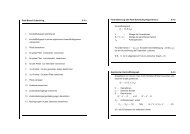
6. When synthesis is complete, view the results by double-clicking<br />
View <strong>Synthesis</strong> Report. Following is a portion of a sample<br />
report.<br />
1-4 <strong>Xilinx</strong> Development System
Figure 1-1 View <strong>Synthesis</strong> Report<br />
Introduction<br />
XST <strong>User</strong> <strong>Guide</strong> 1-5
XST <strong>User</strong> <strong>Guide</strong><br />
1-6 <strong>Xilinx</strong> Development System
HDL Coding Techniques<br />
This chapter contains the following sections:<br />
• “Introduction”<br />
• “Signed/Unsigned Support”<br />
• “Registers”<br />
• “Tristates”<br />
• “Counters”<br />
• “Accumulators”<br />
• “Shift Registers”<br />
• “Dynamic Shift Register”<br />
• “Multiplexers”<br />
• “Decoders”<br />
• “Priority Encoders”<br />
• “Logical Shifters”<br />
• “Arithmetic Operations”<br />
• “RAMs”<br />
• “State Machines”<br />
• “Black Box Support”<br />
Chapter 2<br />
XST <strong>User</strong> <strong>Guide</strong> 2-1
XST <strong>User</strong> <strong>Guide</strong><br />
Introduction<br />
Designs are usually made up of combinatorial logic and macros (for<br />
example, flip-flops, adders, subtractors, counters, FSMs, RAMs). The<br />
macros greatly improve performance of the synthesized designs.<br />
Therefore, it is important to use some coding techniques to model the<br />
macros so that they will be optimally processed by XST.<br />
During its run, XST first of all tries to recognize (infer) as many<br />
macros as possible. Then all of these macros are passed to the low<br />
level optimization step, either preserved as separate blocks or<br />
merged with surrounded logic in order to get better optimization<br />
results. This filtering depends on the type and size of a macro (for<br />
example, by default, 2-to-1 multiplexers are not preserved by the<br />
optimization engine). You have full control of the processing of<br />
inferred macros through synthesis constraints.<br />
Note Please refer to the “Design Constraints” chapter for more details<br />
on constraints and their utilization.<br />
There is detailed information about the macro processing in the XST<br />
LOG file. It contains the following:<br />
• The set of macros and associated signals, inferred by XST from<br />
the VHDL/Verilog source on a block by block basis.<br />
• The overall statistics of recognized macros.<br />
• The number and type of macros preserved by low level<br />
optimization.<br />
2-2 <strong>Xilinx</strong> Development System
HDL Coding Techniques<br />
The following log sample displays the set of recognized macros on a<br />
block by block basis.<br />
Synthesizing Unit .<br />
Related source file is timecore.vhd.<br />
Found finite state machine for signal .<br />
...<br />
Found 7-bit subtractor for signal .<br />
Found 7-bit subtractor for signal .<br />
Found 7-bit register for signal .<br />
Found 4-bit register for signal .<br />
...<br />
Summary:<br />
inferred 1 Finite State Machine(s).<br />
inferred 18 D-type flip-flop(s).<br />
inferred 10 Adder/Subtracter(s).<br />
Unit synthesized.<br />
...<br />
Synthesizing Unit .<br />
Related source file is divider.vhd.<br />
Found 18-bit up counter for signal .<br />
Found 1 1-bit 2-to-1 multiplexers.<br />
Summary:<br />
inferred 1 Counter(s).<br />
inferred 1 Multiplexer(s).<br />
Unit synthesized. ...<br />
XST <strong>User</strong> <strong>Guide</strong> 2-3
XST <strong>User</strong> <strong>Guide</strong><br />
The following log sample displays the overall statistics of recognized<br />
macros.<br />
...<br />
===============================================<br />
HDL <strong>Synthesis</strong> Report<br />
Macro Statistics<br />
# FSMs : 1<br />
# ROMs : 4<br />
16x7-bit ROM : 4<br />
# Registers : 3<br />
7-bit register : 2<br />
4-bit register : 1<br />
# Counters : 1<br />
18-bit up counter : 1<br />
# Multiplexers : 1<br />
2-to-1 multiplexer : 1<br />
# Adders/Subtractors : 10<br />
7-bit adder : 4<br />
7-bit subtractor : 6<br />
===============================================<br />
...<br />
2-4 <strong>Xilinx</strong> Development System
HDL Coding Techniques<br />
The following log sample displays the number and type of macros<br />
preserved by the low level optimization.<br />
...<br />
===============================================<br />
Final Results<br />
...<br />
Macro Statistics<br />
# FSMs : 1<br />
# ROMs : 4<br />
16x7-bit ROM : 4<br />
# Registers : 7<br />
7-bit register : 2<br />
1-bit register : 4<br />
18-bit register : 1<br />
# Adders/Subtractors : 11<br />
7-bit adder : 4<br />
7-bit subtractor : 6<br />
18-bit adder : 1<br />
...<br />
===============================================<br />
...<br />
XST <strong>User</strong> <strong>Guide</strong> 2-5
XST <strong>User</strong> <strong>Guide</strong><br />
This chapter discusses the following Macro Blocks:<br />
• Registers<br />
• Tristates<br />
• Counters<br />
• Accumulators<br />
• Shift Registers<br />
• Dynamic Shift Registers<br />
• Multiplexers<br />
• Decoders<br />
• Priority Encoders<br />
• Logical Shifters<br />
• Arithmetic Operators (Adders, Subtractors, Adders/Subtractors,<br />
Comparators, Multipliers, Dividers, Resource Sharing)<br />
• RAMs<br />
• State Machines<br />
• Black Boxes<br />
For each macro, both VHDL and Verilog examples are given. There is<br />
also a list of constraints you can use to control the macro processing<br />
in XST.<br />
Note For macro implementation details please refer to the “FPGA<br />
Optimization” chapter and the “CPLD Optimization” chapter.<br />
Table 2-1 provides a list of all the examples in this chapter, as well as a<br />
list of VHDL and Verilog synthesis templates available from the<br />
Language Templates in the Project Navigator.<br />
To access the synthesis templates from the Project Navigator:<br />
1. Select Edit → Language Templates...<br />
2. Click the + sign for either VHDL or Verilog.<br />
3. Click the + sign next to <strong>Synthesis</strong> Templates.<br />
2-6 <strong>Xilinx</strong> Development System
Table 2-1 VHDL and Verilog Examples and Templates<br />
HDL Coding Techniques<br />
Macro Blocks Chapter Examples Language Templates<br />
Registers Flip-flop with Positive-Edge<br />
Clock<br />
Flip-flop with Negative-<br />
Edge Clock and Asynchronous<br />
Clear<br />
Flip-flop with Positive-Edge<br />
Clock and Synchronous Set<br />
Flip-flop with Positive-Edge<br />
Clock and Clock Enable<br />
Latch with Positive Gate<br />
Latch with Positive Gate and<br />
Asynchronous Clear<br />
Latch with Positive Gate and<br />
Asynchronous Clear<br />
4-bit Latch with Inverted<br />
Gate and Asynchronous<br />
Preset<br />
4-bit Register with Positive-<br />
Edge Clock, Asynchronous<br />
Set and Clock Enable<br />
Tristates Description Using Combinatorial<br />
Process and Always<br />
Block<br />
Description Using Concurrent<br />
Assignment<br />
D Flip-Flop<br />
D Flip-flop with Asynchronous<br />
Reset<br />
D Flip-Flop with Synchronous<br />
Reset<br />
D Flip-Flop with Clock Enable<br />
D Latch<br />
D Latch with Reset<br />
Process Method (VHDL)<br />
Always Method (Verilog)<br />
Standalone Method (VHDL and<br />
Verilog)<br />
XST <strong>User</strong> <strong>Guide</strong> 2-7
XST <strong>User</strong> <strong>Guide</strong><br />
Table 2-1 VHDL and Verilog Examples and Templates<br />
Macro Blocks Chapter Examples Language Templates<br />
Counters 4-bit Unsigned Up Counter<br />
with Asynchronous Clear<br />
4-bit Unsigned Down<br />
Counter with Synchronous<br />
Set<br />
4-bit Unsigned Up Counter<br />
with Asynchronous Load<br />
from Primary Input<br />
4-bit Unsigned Up Counter<br />
with Synchronous Load with<br />
a Constant<br />
4-bit Unsigned Up Counter<br />
with Asynchronous Clear<br />
and Clock Enable<br />
4-bit Unsigned Up/Down<br />
counter with Asynchronous<br />
Clear<br />
4-bit Signed Up Counter<br />
with Asynchronous Reset<br />
Accumulators 4-bit Unsigned Up Accumulator<br />
with Asynchronous<br />
Clear<br />
4-bit asynchronous counter with<br />
count enable, asynchronous reset<br />
and synchronous load<br />
None<br />
2-8 <strong>Xilinx</strong> Development System
Table 2-1 VHDL and Verilog Examples and Templates<br />
Shift Registers 8-bit Shift-Left Register with<br />
Positive-Edge Clock, Serial<br />
In, and Serial Out<br />
8-bit Shift-Left Register with<br />
Negative-Edge Clock, Clock<br />
Enable, Serial In, and Serial<br />
Out<br />
8-bit Shift-Left Register with<br />
Positive-Edge Clock, Asynchronous<br />
Clear, Serial In, and<br />
Serial Out<br />
8-bit Shift-Left Register with<br />
Positive-Edge Clock,<br />
Synchronous Set, Serial In,<br />
and Serial Out<br />
8-bit Shift-Left Register with<br />
Positive-Edge Clock, Serial<br />
In, and Parallel Out<br />
8-bit Shift-Left Register with<br />
Positive-Edge Clock, Asynchronous<br />
Parallel Load,<br />
Serial In, and Serial Out<br />
8-bit Shift-Left Register with<br />
Positive-Edge Clock,<br />
Synchronous Parallel Load,<br />
Serial In, and Serial Out<br />
8-bit Shift-Left/Shift-Right<br />
Register with Positive-Edge<br />
Clock, Serial In, and Parallel<br />
Out<br />
HDL Coding Techniques<br />
Macro Blocks Chapter Examples Language Templates<br />
4-bit Loadable Serial In Serial<br />
Out Shift Register<br />
4-bit Serial In Parallel out Shift<br />
Register<br />
4-bit Serial In Serial Out Shift<br />
Register<br />
XST <strong>User</strong> <strong>Guide</strong> 2-9
XST <strong>User</strong> <strong>Guide</strong><br />
Table 2-1 VHDL and Verilog Examples and Templates<br />
Macro Blocks Chapter Examples Language Templates<br />
Multiplexers 4-to-1 1-bit MUX using IF<br />
Statement<br />
4-to-1 MUX Using CASE<br />
Statement<br />
4-to-1 MUX Using Tristate<br />
Buffers<br />
No 4-to-1 MUX<br />
Decoders VHDL (One-Hot)<br />
Verilog (One-Hot)<br />
VHDL (One-Cold)<br />
Verilog (One-Cold)<br />
4-to-1 MUX Design with CASE<br />
Statement<br />
4-to-1 MUX Design with Tristate<br />
Construct<br />
1-of-8 Decoder, Synchronous<br />
with Reset<br />
Priority Encoders 3-Bit 1-of-9 Priority Encoder 8-to-3 encoder, Synchronous<br />
with Reset<br />
Logical Shifters Example 1<br />
Example 2<br />
Example 3<br />
None<br />
Dynamic Shifters 16-bit Dynamic Shift Register<br />
with Positive-Edge Clock,<br />
Serial In and Serial Out<br />
None<br />
2-10 <strong>Xilinx</strong> Development System
Table 2-1 VHDL and Verilog Examples and Templates<br />
Arithmetic Operators Unsigned 8-bit Adder<br />
Unsigned 8-bit Adder with<br />
Carry In<br />
Unsigned 8-bit Adder with<br />
Carry Out<br />
Unsigned 8-bit Adder with<br />
Carry In and Carry Out<br />
Simple Signed 8-bit Adder<br />
Unsigned 8-bit Subtractor<br />
Unsigned 8-bit Adder/<br />
Subtractor<br />
Unsigned 8-bit Greater or<br />
Equal Comparator<br />
Unsigned 8x4-bit Multiplier<br />
Division By Constant 2<br />
Resource Sharing<br />
HDL Coding Techniques<br />
Macro Blocks Chapter Examples Language Templates<br />
N-Bit Comparator, Synchronous<br />
with Reset<br />
XST <strong>User</strong> <strong>Guide</strong> 2-11
XST <strong>User</strong> <strong>Guide</strong><br />
Table 2-1 VHDL and Verilog Examples and Templates<br />
Macro Blocks Chapter Examples Language Templates<br />
RAMs Single-Port RAM with Asynchronous<br />
Read<br />
Single-Port RAM with "false"<br />
Synchronous Read<br />
Single-Port RAM with<br />
Synchronous Read (Read<br />
Through)<br />
Dual-Port RAM with Asynchronous<br />
Read<br />
Dual-Port RAM with False<br />
Synchronous Read<br />
Dual-Port RAM with<br />
Synchronous Read (Read<br />
Through)<br />
Dual-Port Block RAM with<br />
Different Clocks<br />
Multiple-Port RAM<br />
Descriptions<br />
State Machines FSM with 1 Process<br />
FSM with 2 Processes<br />
FSM with 3 Processes<br />
Black Boxes VHDL<br />
Verilog<br />
Single-Port Block RAM<br />
Single-Port Distributed RAM<br />
Dual-Port Block RAM<br />
Dual-Port Distributed RAM<br />
Binary State Machine<br />
One-Hot State Machine<br />
None<br />
2-12 <strong>Xilinx</strong> Development System
Signed/Unsigned Support<br />
Registers<br />
HDL Coding Techniques<br />
When using Verilog or VHDL in XST, some macros, such as adders or<br />
counters, can be implemented for signed and unsigned values.<br />
For Verilog, to enable support for signed and unsigned values, you<br />
have to enable Verilog2001. You can enable it by selecting the Verilog<br />
2001option under the <strong>Synthesis</strong> Options tab in the Process Properties<br />
dialog box within the Project Navigator, or by setting the -verilog2001<br />
command line option to yes. See the “VERILOG2001” section in the<br />
Constraints <strong>Guide</strong> for details.<br />
For VHDL, depending on the operation and type of the operands,<br />
you have to include additional packages in your code. For example,<br />
in order to create an unsigned adder, you can use the following<br />
arithmetic packages and types that operate on unsigned values:<br />
PACKAGE TYPE<br />
numeric_std unsigned<br />
std_logic_arith unsigned<br />
std_logic_unsigned std_logic_vector<br />
In order to create a signed adder you can use arithmetic packages and<br />
types that operate on signed values.<br />
PACKAGE TYPE<br />
numeric_std signed<br />
std_logic_arith signed<br />
std_logic_signed std_logic_vector<br />
Please refer to the IEEE VHDL Manual for details on available types.<br />
XST recognizes flip-flops with the following control signals:<br />
• Asynchronous Set/Clear<br />
• Synchronous Set/Clear<br />
• Clock Enable<br />
XST <strong>User</strong> <strong>Guide</strong> 2-13
XST <strong>User</strong> <strong>Guide</strong><br />
Log File<br />
The XST log file reports the type and size of recognized flip-flops<br />
during the macro recognition step.<br />
...<br />
Synthesizing Unit .<br />
Related source file is ff_1.vhd.<br />
Found 1-bit register for signal .<br />
Summary:<br />
inferred 1 D-type flip-flop(s).<br />
Unit synthesized.<br />
...<br />
==============================<br />
HDL <strong>Synthesis</strong> Report<br />
Macro Statistics<br />
# Registers : 1<br />
1-bit register : 1<br />
==============================<br />
...<br />
Related Constraints<br />
A related constraint is IOB.<br />
2-14 <strong>Xilinx</strong> Development System
Flip-flop with Positive-Edge Clock<br />
HDL Coding Techniques<br />
The following figure shows a flip-flop with positive-edge clock.<br />
D<br />
C<br />
FD<br />
The following table shows pin definitions for a flip-flop with positive<br />
edge clock.<br />
IO Pins Description<br />
D Data Input<br />
C Positive Edge Clock<br />
Q Data Output<br />
VHDL Code<br />
Q<br />
X3715<br />
Following is the equivalent VHDL code sample for the flip-flop with<br />
a positive-edge clock.<br />
library ieee;<br />
use ieee.std_logic_1164.all;<br />
entity flop is<br />
port(C, D : in std_logic;<br />
Q : out std_logic);<br />
end flop;<br />
architecture archi of flop is<br />
begin<br />
process (C)<br />
begin<br />
if (C'event and C='1') then<br />
Q
XST <strong>User</strong> <strong>Guide</strong><br />
Note When using VHDL, for a positive-edge clock instead of using<br />
if (C’event and C=’1’) then<br />
you can also use<br />
if (rising_edge(C)) then<br />
and for a negative-edge clock you can use<br />
if (falling_edge(C)) then<br />
or<br />
C’event and C=’0’<br />
Verilog Code<br />
Following is the equivalent Verilog code sample for the flip-flop with<br />
a positive-edge clock.<br />
module flop (C, D, Q);<br />
input C, D;<br />
output Q;<br />
reg Q;<br />
always @(posedge C)<br />
begin<br />
Q = D;<br />
end<br />
endmodule<br />
Flip-flop with Negative-Edge Clock and<br />
Asynchronous Clear<br />
The following figure shows a flip-flop with negative-edge clock and<br />
asynchronous clear.<br />
D<br />
C<br />
CLR<br />
FDC_1<br />
Q<br />
X3847<br />
2-16 <strong>Xilinx</strong> Development System
HDL Coding Techniques<br />
The following table shows pin definitions for a flip-flop with negative<br />
edge clock and asynchronous clear.<br />
IO Pins Description<br />
D Data Input<br />
C Negative-Edge Clock<br />
CLR Asynchronous Clear (active High)<br />
Q Data Output<br />
VHDL Code<br />
Following is the equivalent VHDL code for a flip-flop with a<br />
negative-edge clock and asynchronous clear.<br />
library ieee;<br />
use ieee.std_logic_1164.all;<br />
entity flop is<br />
port(C, D, CLR : in std_logic;<br />
Q : out std_logic);<br />
end flop;<br />
architecture archi of flop is<br />
begin<br />
process (C, CLR)<br />
begin<br />
if (CLR = '1')then<br />
Q
XST <strong>User</strong> <strong>Guide</strong><br />
Verilog Code<br />
Following is the equivalent Verilog code for a flip-flop with a<br />
negative-edge clock and asynchronous clear.<br />
module flop (C, D, CLR, Q);<br />
input C, D, CLR;<br />
output Q;<br />
reg Q;<br />
always @(negedge C or posedge CLR)<br />
begin<br />
if (CLR)<br />
Q = 1’b0;<br />
else<br />
Q = D;<br />
end<br />
endmodule<br />
Flip-flop with Positive-Edge Clock and Synchronous<br />
Set<br />
The following figure shows a flip-flop with positive-edge clock and<br />
synchronous set.<br />
S<br />
D<br />
C<br />
FDS<br />
Q<br />
X3722<br />
The following table shows pin definitions for a flip-flop with positive<br />
edge clock and synchronous set.<br />
IO Pins Description<br />
D Data Input<br />
C Positive-Edge Clock<br />
S Synchronous Set (active High)<br />
Q Data Output<br />
2-18 <strong>Xilinx</strong> Development System
VHDL Code<br />
HDL Coding Techniques<br />
Following is the equivalent VHDL code for the flip-flop with a<br />
positive-edge clock and synchronous set.<br />
library ieee;<br />
use ieee.std_logic_1164.all;<br />
entity flop is<br />
port(C, D, S : in std_logic;<br />
Q : out std_logic);<br />
end flop;<br />
architecture archi of flop is<br />
begin<br />
process (C)<br />
begin<br />
if (C'event and C='1') then<br />
if (S='1') then<br />
Q
XST <strong>User</strong> <strong>Guide</strong><br />
Verilog Code<br />
Following is the equivalent Verilog code for the flip-flop with a<br />
positive-edge clock and synchronous set.<br />
module flop (C, D, S, Q);<br />
input C, D, S;<br />
output Q;<br />
reg Q;<br />
always @(posedge C)<br />
begin<br />
if (S)<br />
Q = 1’b1;<br />
else<br />
Q = D;<br />
end<br />
endmodule<br />
Flip-flop with Positive-Edge Clock and Clock Enable<br />
The following figure shows a flip-flop with positive-edge clock and<br />
clock enable.<br />
D<br />
CE<br />
C<br />
FDE<br />
Q<br />
X8361<br />
2-20 <strong>Xilinx</strong> Development System
HDL Coding Techniques<br />
The following table shows pin definitions for a flip-flop with positive<br />
edge clock and clock enable.<br />
IO Pins Description<br />
D Data Input<br />
C Positive-Edge Clock<br />
CE Clock Enable (active High)<br />
Q Data Output<br />
VHDL Code<br />
Following is the equivalent VHDL code for the flip-flop with a<br />
positive-edge clock and clock Enable.<br />
library ieee;<br />
use ieee.std_logic_1164.all;<br />
entity flop is<br />
port(C, D, CE : in std_logic;<br />
Q : out std_logic);<br />
end flop;<br />
architecture archi of flop is<br />
begin<br />
process (C)<br />
begin<br />
if (C'event and C='1') then<br />
if (CE='1') then<br />
Q
XST <strong>User</strong> <strong>Guide</strong><br />
Verilog Code<br />
Following is the equivalent Verilog code for the flip-flop with a<br />
positive-edge clock and clock enable.<br />
module flop (C, D, CE, Q);<br />
input C, D, CE;<br />
output Q;<br />
reg Q;<br />
always @(posedge C)<br />
begin<br />
if (CE)<br />
Q = D;<br />
end<br />
endmodule<br />
4-bit Register with Positive-Edge Clock,<br />
Asynchronous Set and Clock Enable<br />
The following figure shows a 4-bit register with positive-edge clock,<br />
asynchronous set and clock enable.<br />
PRE<br />
D<br />
CE<br />
C<br />
FDPE<br />
Q<br />
X3721<br />
The following table shows pin definitions for a 4-bit register with<br />
positive-edge clock, asynchronous set and clock enable.<br />
IO Pins Description<br />
D[3:0] Data Input<br />
C Positive-Edge Clock<br />
PRE Asynchronous Set (active High)<br />
2-22 <strong>Xilinx</strong> Development System
IO Pins Description<br />
CE Clock Enable (active High)<br />
Q[3:0] Data Output<br />
VHDL Code<br />
HDL Coding Techniques<br />
Following is the equivalent VHDL code for a 4-bit register with a<br />
positive-edge clock, asynchronous set and clock enable.<br />
library ieee;<br />
use ieee.std_logic_1164.all;<br />
entity flop is<br />
port(C, CE, PRE : in std_logic;<br />
D : in std_logic_vector (3 downto 0);<br />
Q : out std_logic_vector (3 downto 0));<br />
end flop;<br />
architecture archi of flop is<br />
begin<br />
process (C, PRE)<br />
begin<br />
if (PRE='1') then<br />
Q
XST <strong>User</strong> <strong>Guide</strong><br />
Latches<br />
Verilog Code<br />
Following is the equivalent Verilog code for a 4-bit register with a<br />
positive-edge clock, asynchronous set and clock enable.<br />
module flop (C, D, CE, PRE, Q);<br />
input C, CE, PRE;<br />
input [3:0] D;<br />
output [3:0] Q;<br />
reg [3:0] Q;<br />
always @(posedge C or posedge PRE)<br />
begin<br />
if (PRE)<br />
Q = 4'b1111;<br />
else<br />
if (CE)<br />
Q = D;<br />
end<br />
endmodule<br />
XST is able to recognize latches with the asynchronous set/clear<br />
control signals.<br />
Latches can be described using:<br />
• Process (VHDL) and always block (Verilog)<br />
• Concurrent state assignment<br />
2-24 <strong>Xilinx</strong> Development System
Log File<br />
HDL Coding Techniques<br />
The XST log file reports the type and size of recognized latches<br />
during the macro recognition step.<br />
...<br />
Synthesizing Unit .<br />
Related source file is latch_1.vhd.<br />
WARNING:Xst:737 - Found 1-bit latch for signal .<br />
Summary:<br />
inferred 1 Latch(s).<br />
Unit synthesized.<br />
==============================<br />
HDL <strong>Synthesis</strong> Report<br />
Macro Statistics<br />
# Latches : 1<br />
1-bit latch : 1<br />
==============================<br />
...<br />
Related Constraints<br />
A related constraint is IOB.<br />
XST <strong>User</strong> <strong>Guide</strong> 2-25
XST <strong>User</strong> <strong>Guide</strong><br />
Latch with Positive Gate<br />
The following figure shows a latch with positive gate.<br />
D<br />
G<br />
LD<br />
X3740<br />
Q<br />
The following table shows pin definitions for a latch with positive<br />
gate.<br />
IO Pins Description<br />
D Data Input<br />
G Positive Gate<br />
Q Data Output<br />
VHDL Code<br />
Following is the equivalent VHDL code for a latch with a positive<br />
gate.<br />
library ieee;<br />
use ieee.std_logic_1164.all;<br />
entity latch is<br />
port(G, D : in std_logic;<br />
Q : out std_logic);<br />
end latch;<br />
architecture archi of latch is<br />
begin<br />
process (G, D)<br />
begin<br />
if (G='1') then<br />
Q
HDL Coding Techniques<br />
Verilog Code<br />
Following is the equivalent Verilog code for a latch with a positive<br />
gate.<br />
module latch (G, D, Q);<br />
input G, D;<br />
output Q;<br />
reg Q;<br />
always @(G or D)<br />
begin<br />
if (G)<br />
Q = D;<br />
end<br />
endmodule<br />
Latch with Positive Gate and Asynchronous Clear<br />
The following figure shows a latch with positive gate and<br />
asynchronous clear.<br />
D<br />
G<br />
CLR<br />
LDC<br />
X4070<br />
Q<br />
The following table shows pin definitions for a latch with positive<br />
gate and asynchronous clear.<br />
IO Pins Description<br />
D Data Input<br />
G Positive Gate<br />
CLR Asynchronous Clear (active High)<br />
Q Data Output<br />
XST <strong>User</strong> <strong>Guide</strong> 2-27
XST <strong>User</strong> <strong>Guide</strong><br />
VHDL Code<br />
Following is the equivalent VHDL code for a latch with a positive<br />
gate and asynchronous clear.<br />
library ieee;<br />
use ieee.std_logic_1164.all;<br />
entity latch is<br />
port(G, D, CLR : in std_logic;<br />
Q : out std_logic);<br />
end latch;<br />
architecture archi of latch is<br />
begin<br />
process (CLR, D, G)<br />
begin<br />
if (CLR='1') then<br />
Q
HDL Coding Techniques<br />
4-bit Latch with Inverted Gate and Asynchronous<br />
Preset<br />
The following figure shows a 4-bit latch with inverted gate and<br />
asynchronous preset.<br />
PRE<br />
D<br />
G<br />
LDP_1<br />
The following table shows pin definitions for a latch with inverted<br />
gate and asynchronous preset.<br />
IO Pins Description<br />
D[3:0] Data Input<br />
G Inverted Gate<br />
PRE Asynchronous Preset (active High)<br />
Q[3:0] Data Output<br />
VHDL Code<br />
Q<br />
X8376<br />
Following is the equivalent VHDL code for a 4-bit latch with an<br />
inverted gate and asynchronous preset.<br />
XST <strong>User</strong> <strong>Guide</strong> 2-29
XST <strong>User</strong> <strong>Guide</strong><br />
library ieee;<br />
use ieee.std_logic_1164.all;<br />
entity latch is<br />
port(D : in std_logic_vector(3 downto 0);<br />
G, PRE : in std_logic;<br />
Q : out std_logic_vector(3 downto 0));<br />
end latch;<br />
architecture archi of latch is<br />
begin<br />
process (PRE, G)<br />
begin<br />
if (PRE='1') then<br />
Q
Tristates<br />
Log File<br />
HDL Coding Techniques<br />
Tristate elements can be described using the following:<br />
• Combinatorial process (VHDL) and always block (Verilog)<br />
• Concurrent assignment<br />
The XST log reports the type and size of recognized tristates during<br />
the macro recognition step.<br />
...<br />
Synthesizing Unit .<br />
Related source file is tristates_1.vhd.<br />
Found 1-bit tristate buffer for signal .<br />
Summary:<br />
inferred 1 Tristate(s).<br />
Unit synthesized.<br />
=============================<br />
HDL <strong>Synthesis</strong> Report<br />
Macro Statistics<br />
# Tristates : 1<br />
1-bit tristate buffer : 1<br />
=============================<br />
...<br />
Related Constraints<br />
There are no related constraints available.<br />
XST <strong>User</strong> <strong>Guide</strong> 2-31
XST <strong>User</strong> <strong>Guide</strong><br />
Description Using Combinatorial Process and<br />
Always Block<br />
The following figure shows a tristate element using combinatorial<br />
process and always block.<br />
The following table shows pin definitions for a tristate element using<br />
combinatorial process and always block.<br />
IO Pins Description<br />
I Data Input<br />
T Output Enable (active Low)<br />
O Data Output<br />
2-32 <strong>Xilinx</strong> Development System
VHDL Code<br />
HDL Coding Techniques<br />
Following is VHDL code for a tristate element using a combinatorial<br />
process and always block.<br />
library ieee;<br />
use ieee.std_logic_1164.all;<br />
entity three_st is<br />
port(T : in std_logic;<br />
I : in std_logic;<br />
O : out std_logic);<br />
end three_st;<br />
architecture archi of three_st is<br />
begin<br />
process (I, T)<br />
begin<br />
if (T='0') then<br />
O
XST <strong>User</strong> <strong>Guide</strong><br />
Description Using Concurrent Assignment<br />
In the following two examples, note that comparing to 0 instead of 1<br />
will infer the BUFT primitive instead of the BUFE macro. (The BUFE<br />
macro has an inverter on the E pin.)<br />
VHDL Code<br />
Following is VHDL code for a tristate element using a concurrent<br />
assignment.<br />
library ieee;<br />
use ieee.std_logic_1164.all;<br />
entity three_st is<br />
port(T : in std_logic;<br />
I: in std_logic;<br />
O: out std_logic);<br />
end three_st;<br />
architecture archi of three_st is<br />
begin<br />
O
Counters<br />
HDL Coding Techniques<br />
XST is able to recognize counters with the following control signals:<br />
• Asynchronous Set/Clear<br />
• Synchronous Set/Clear<br />
• Asynchronous/Synchronous Load (signal and/or constant)<br />
• Clock Enable<br />
• Modes (Up, Down, Up/Down)<br />
• Mixture of all of the above possibilities<br />
HDL coding styles for the following control signals are equivalent to<br />
the ones described in the “Registers” section of this chapter:<br />
• Clock<br />
• Asynchronous Set/Clear<br />
• Synchronous Set/Clear<br />
• Clock Enable<br />
Moreover, XST supports both unsigned and signed counters.<br />
XST <strong>User</strong> <strong>Guide</strong> 2-35
XST <strong>User</strong> <strong>Guide</strong><br />
Log File<br />
The XST log file reports the type and size of recognized counters<br />
during the macro recognition step.<br />
...<br />
Synthesizing Unit .<br />
Related source file is counters_1.vhd.<br />
Found 4-bit up counter for signal .<br />
Summary:<br />
inferred 1 Counter(s).<br />
Unit synthesized.<br />
==============================<br />
HDL <strong>Synthesis</strong> Report<br />
Macro Statistics<br />
# Counters : 1<br />
4-bit up counter : 1<br />
==============================<br />
...<br />
Note During synthesis, XST decomposes Counters on Adders and<br />
Registers if they do not contain synchronous load signals. This is<br />
done to create additional opportunities for timing optimization.<br />
Because of this, counters reported during the recognition step and in<br />
the overall statistics of recognized macros may not appear in the final<br />
report. Adders/registers are reported instead.<br />
4-bit Unsigned Up Counter with Asynchronous Clear<br />
The following table shows pin definitions for a 4-bit unsigned up<br />
counter with asynchronous clear.<br />
IO Pins Description<br />
C Positive-Edge Clock<br />
CLR Asynchronous Clear (active High)<br />
Q[3:0] Data Output<br />
2-36 <strong>Xilinx</strong> Development System
VHDL Code<br />
HDL Coding Techniques<br />
Following is VHDL code for a 4-bit unsigned up counter with<br />
asynchronous clear.<br />
library ieee;<br />
use ieee.std_logic_1164.all;<br />
use ieee.std_logic_unsigned.all;<br />
entity counter is<br />
port(C, CLR : in std_logic;<br />
Q : out std_logic_vector(3 downto 0));<br />
end counter;<br />
architecture archi of counter is<br />
signal tmp: std_logic_vector(3 downto 0);<br />
begin<br />
process (C, CLR)<br />
begin<br />
if (CLR='1') then<br />
tmp
XST <strong>User</strong> <strong>Guide</strong><br />
Verilog Code<br />
Following is the Verilog code for a 4-bit unsigned up counter with<br />
asynchronous clear.<br />
module counter (C, CLR, Q);<br />
input C, CLR;<br />
output [3:0] Q;<br />
reg [3:0] tmp;<br />
always @(posedge C or posedge CLR)<br />
begin<br />
if (CLR)<br />
tmp = 4'b0000;<br />
else<br />
tmp = tmp + 1'b1;<br />
end<br />
assign Q = tmp;<br />
endmodule<br />
2-38 <strong>Xilinx</strong> Development System
HDL Coding Techniques<br />
4-bit Unsigned Down Counter with Synchronous Set<br />
The following table shows pin definitions for a 4-bit unsigned down<br />
counter with synchronous set.<br />
IO Pins Description<br />
C Positive-Edge Clock<br />
S Synchronous Set (active High)<br />
Q[3:0] Data Output<br />
VHDL Code<br />
Following is the VHDL code for a 4-bit unsigned down counter with<br />
synchronous set.<br />
library ieee;<br />
use ieee.std_logic_1164.all;<br />
use ieee.std_logic_unsigned.all;<br />
entity counter is<br />
port(C, S : in std_logic;<br />
Q : out std_logic_vector(3 downto 0));<br />
end counter;<br />
architecture archi of counter is<br />
signal tmp: std_logic_vector(3 downto 0);<br />
begin<br />
process (C)<br />
begin<br />
if (C'event and C='1') then<br />
if (S='1') then<br />
tmp
XST <strong>User</strong> <strong>Guide</strong><br />
Verilog Code<br />
Following is the Verilog code for a 4-bit unsigned down counter with<br />
synchronous set.<br />
module counter (C, S, Q);<br />
input C, S;<br />
output [3:0] Q;<br />
reg [3:0] tmp;<br />
always @(posedge C)<br />
begin<br />
if (S)<br />
tmp = 4'b1111;<br />
else<br />
tmp = tmp - 1'b1;<br />
end<br />
assign Q = tmp;<br />
endmodule<br />
4-bit Unsigned Up Counter with Asynchronous Load<br />
from Primary Input<br />
The following table shows pin definitions for a 4-bit unsigned up<br />
counter with asynchronous load from primary input.<br />
IO Pins Description<br />
C Positive-Edge Clock<br />
ALOAD Asynchronous Load (active High)<br />
D[3:0] Data Input<br />
Q[3:0] Data Output<br />
VHDL Code<br />
Following is the VHDL code for a 4-bit unsigned up counter with<br />
asynchronous load from primary input.<br />
library ieee;<br />
use ieee.std_logic_1164.all;<br />
use ieee.std_logic_unsigned.all;<br />
2-40 <strong>Xilinx</strong> Development System
HDL Coding Techniques<br />
entity counter is<br />
port(C, ALOAD : in std_logic;<br />
D : in std_logic_vector(3 downto 0);<br />
Q : out std_logic_vector(3 downto 0));<br />
end counter;<br />
architecture archi of counter is<br />
signal tmp: std_logic_vector(3 downto 0);<br />
begin<br />
process (C, ALOAD, D)<br />
begin<br />
if (ALOAD='1') then<br />
tmp
XST <strong>User</strong> <strong>Guide</strong><br />
4-bit Unsigned Up Counter with Synchronous Load<br />
with a Constant<br />
The following table shows pin definitions for a 4-bit unsigned up<br />
counter with synchronous load with a constant.<br />
IO Pins Description<br />
C Positive-Edge Clock<br />
SLOAD Synchronous Load (active High)<br />
Q[3:0] Data Output<br />
VHDL Code<br />
Following is the VHDL code for a 4-bit unsigned up counter with<br />
synchronous load with a constant.<br />
library ieee;<br />
use ieee.std_logic_1164.all;<br />
use ieee.std_logic_unsigned.all;<br />
entity counter is<br />
port(C, SLOAD : in std_logic;<br />
Q : out std_logic_vector(3 downto 0));<br />
end counter;<br />
architecture archi of counter is<br />
signal tmp: std_logic_vector(3 downto 0);<br />
begin<br />
process (C)<br />
begin<br />
if (C'event and C='1') then<br />
if (SLOAD='1') then<br />
tmp
Verilog Code<br />
HDL Coding Techniques<br />
Following is the Verilog code for a 4-bit unsigned up counter with<br />
synchronous load with a constant.<br />
module counter (C, SLOAD, Q);<br />
input C, SLOAD;<br />
output [3:0] Q;<br />
reg [3:0] tmp;<br />
always @(posedge C)<br />
begin<br />
if (SLOAD)<br />
tmp = 4'b1010;<br />
else<br />
tmp = tmp + 1'b1;<br />
end<br />
assign Q = tmp;<br />
endmodule<br />
4-bit Unsigned Up Counter with Asynchronous Clear<br />
and Clock Enable<br />
The following table shows pin definitions for a 4-bit unsigned up<br />
counter with asynchronous clear and clock enable.<br />
IO Pins Description<br />
C Positive-Edge Clock<br />
CLR Asynchronous Clear (active High)<br />
CE Clock Enable<br />
Q[3:0] Data Output<br />
VHDL Code<br />
Following is the VHDL code for a 4-bit unsigned up counter with<br />
asynchronous clear and clock enable.<br />
library ieee;<br />
use ieee.std_logic_1164.all;<br />
use ieee.std_logic_unsigned.all;<br />
XST <strong>User</strong> <strong>Guide</strong> 2-43
XST <strong>User</strong> <strong>Guide</strong><br />
entity counter is<br />
port(C, CLR, CE : in std_logic;<br />
Q : out std_logic_vector(3 downto 0));<br />
end counter;<br />
architecture archi of counter is<br />
signal tmp: std_logic_vector(3 downto 0);<br />
begin<br />
process (C, CLR)<br />
begin<br />
if (CLR='1') then<br />
tmp
HDL Coding Techniques<br />
4-bit Unsigned Up/Down counter with Asynchronous<br />
Clear<br />
The following table shows pin definitions for a 4-bit unsigned up/<br />
down counter with asynchronous clear.<br />
IO Pins Description<br />
C Positive-Edge Clock<br />
CLR Asynchronous Clear (active High)<br />
UP_DOWN up/down count mode selector<br />
Q[3:0] Data Output<br />
VHDL Code<br />
Following is the VHDL code for a 4-bit unsigned up/down counter<br />
with asynchronous clear.<br />
library ieee;<br />
use ieee.std_logic_1164.all;<br />
use ieee.std_logic_unsigned.all;<br />
entity counter is<br />
port(C, CLR, UP_DOWN : in std_logic;<br />
Q : out std_logic_vector(3 downto 0));<br />
end counter;<br />
architecture archi of counter is<br />
signal tmp: std_logic_vector(3 downto 0);<br />
begin<br />
process (C, CLR)<br />
begin<br />
if (CLR='1') then<br />
tmp
XST <strong>User</strong> <strong>Guide</strong><br />
Verilog Code<br />
Following is the Verilog code for a 4-bit unsigned up/down counter<br />
with asynchronous clear.<br />
module counter (C, CLR, UP_DOWN, Q);<br />
input C, CLR, UP_DOWN;<br />
output [3:0] Q;<br />
reg [3:0] tmp;<br />
always @(posedge C or posedge CLR)<br />
begin<br />
if (CLR)<br />
tmp = 4'b0000;<br />
else<br />
if (UP_DOWN)<br />
tmp = tmp + 1'b1;<br />
else<br />
tmp = tmp - 1'b1;<br />
end<br />
assign Q = tmp;<br />
endmodule<br />
4-bit Signed Up Counter with Asynchronous Reset<br />
The following table shows pin definitions for a 4-bit signed up<br />
counter with asynchronous reset.<br />
IO Pins Description<br />
C Positive-Edge Clock<br />
CLR Asynchronous Clear (active High)<br />
Q[3:0] Data Output<br />
2-46 <strong>Xilinx</strong> Development System
VHDL Code<br />
HDL Coding Techniques<br />
Following is the VHDL code for a 4-bit signed up counter with<br />
asynchronous reset.<br />
library ieee;<br />
use ieee.std_logic_1164.all;<br />
use ieee.std_logic_signed.all;<br />
entity counter is<br />
port(C, CLR : in std_logic;<br />
Q : out std_logic_vector(3 downto 0));<br />
end counter;<br />
architecture archi of counter is<br />
signal tmp: std_logic_vector(3 downto 0);<br />
begin<br />
process (C, CLR)<br />
begin<br />
if (CLR='1') then<br />
tmp
XST <strong>User</strong> <strong>Guide</strong><br />
Verilog Code<br />
Following is the Verilog code for a 4-bit signed up counter with<br />
asynchronous reset.<br />
module counter (C, CLR, Q);<br />
input C, CLR;<br />
output signed [3:0] Q;<br />
reg signed [3:0] tmp;<br />
always @ (posedge C or posedge CLR)<br />
begin<br />
if (CLR)<br />
tmp
Accumulators<br />
HDL Coding Techniques<br />
An accumulator differs from a counter in the nature of the operands<br />
of the add and subtract operation:<br />
• In a counter, the destination and first operand is a signal or<br />
variable and the other operand is a constant equal to 1:<br />
A
XST <strong>User</strong> <strong>Guide</strong><br />
Log File<br />
The XST log file reports the type and size of recognized accumulators<br />
during the macro recognition step.<br />
...<br />
Synthesizing Unit .<br />
Related source file is accumulators_1.vhd.<br />
Found 4-bit up accumulator for signal .<br />
Summary:<br />
inferred 1 Accumulator(s).<br />
Unit synthesized.<br />
==============================<br />
HDL <strong>Synthesis</strong> Report<br />
Macro Statistics<br />
# Accumulators : 1<br />
4-bit up accumulator : 1<br />
==============================<br />
...<br />
Note During synthesis, XST decomposes Accumulators on Adders<br />
and Registers if they do not contain synchronous load signals. This is<br />
done to create additional opportunities for timing optimization.<br />
Because of this, Accumulators reported during the recognition step<br />
and in the overall statistics of recognized macros may not appear in<br />
the final report. Adders/registers are reported instead.<br />
4-bit Unsigned Up Accumulator with Asynchronous<br />
Clear<br />
The following table shows pin definitions for a 4-bit unsigned up<br />
accumulator with asynchronous clear.<br />
IO Pins Description<br />
C Positive-Edge Clock<br />
CLR Asynchronous Clear (active High)<br />
D[3:0] Data Input<br />
Q[3:0] Data Output<br />
2-50 <strong>Xilinx</strong> Development System
VHDL Code<br />
HDL Coding Techniques<br />
Following is the VHDL code for a 4-bit unsigned up accumulator<br />
with asynchronous clear.<br />
library ieee;<br />
use ieee.std_logic_1164.all;<br />
use ieee.std_logic_unsigned.all;<br />
entity accum is<br />
port(C, CLR : in std_logic;<br />
D : in std_logic_vector(3 downto 0);<br />
Q : out std_logic_vector(3 downto 0));<br />
end accum;<br />
architecture archi of accum is<br />
signal tmp: std_logic_vector(3 downto 0);<br />
begin<br />
process (C, CLR)<br />
begin<br />
if (CLR='1') then<br />
tmp
XST <strong>User</strong> <strong>Guide</strong><br />
Shift Registers<br />
Verilog Code<br />
Following is the Verilog code for a 4-bit unsigned up accumulator<br />
with asynchronous clear.<br />
module accum (C, CLR, D, Q);<br />
input C, CLR;<br />
input [3:0] D;<br />
output [3:0] Q;<br />
reg [3:0] tmp;<br />
always @(posedge C or posedge CLR)<br />
begin<br />
if (CLR)<br />
tmp = 4'b0000;<br />
else<br />
tmp = tmp + D;<br />
end<br />
assign Q = tmp;<br />
endmodule<br />
No constraints are available.<br />
In general a shift register is characterized by the following control<br />
and data signals, which are fully recognized by XST:<br />
• clock<br />
• serial input<br />
• asynchronous set/reset<br />
• synchronous set/reset<br />
• synchronous/asynchronous parallel load<br />
• clock enable<br />
• serial or parallel output. The shift register output mode may be:<br />
♦ serial: only the contents of the last flip-flop are accessed by<br />
the rest of the circuit<br />
♦ parallel: the contents of one or several flip-flops, other than<br />
the last one, are accessed<br />
2-52 <strong>Xilinx</strong> Development System
HDL Coding Techniques<br />
• shift modes: left, right, etc.<br />
There are different ways to describe shift registers. For example, in<br />
VHDL you can use:<br />
• concatenation operator<br />
shreg
XST <strong>User</strong> <strong>Guide</strong><br />
The following figure shows the pin layout of SRLC16.<br />
D<br />
CLK<br />
A0<br />
A1<br />
A2<br />
A3<br />
SRLC16<br />
X9497<br />
Note Synchronous and asynchronous control signals are not<br />
available in the SLRC16x primitives.<br />
SRL16 and SRLC16 support only LEFT shift operation for a limited<br />
number of IO signals.<br />
• Clock<br />
• Clock enable<br />
• Serial data in<br />
• Serial data out<br />
This means that if your shift register does have, for instance, a<br />
synchronous parallel load, no SRL16 will be implemented. XST will<br />
not try to infer SR4x, SR8x or SR16x macros. It will use specific<br />
internal processing which allows it to produce the best final results.<br />
The XST log file reports recognized shift registers when it can be<br />
implemented using SRL16.<br />
2-54 <strong>Xilinx</strong> Development System<br />
Q<br />
Q15
Log File<br />
HDL Coding Techniques<br />
The XST log file reports the type and size of recognized shift registers<br />
during the macro recognition step.<br />
...<br />
Synthesizing Unit .<br />
Related source file is shift_registers_1.vhd.<br />
Found 8-bit shift register for signal .<br />
Summary:<br />
inferred 1 Shift register(s).<br />
Unit synthesized.<br />
==============================<br />
HDL <strong>Synthesis</strong> Report<br />
Macro Statistics<br />
# Shift Registers : 1<br />
8-bit shift register : 1<br />
==============================<br />
...<br />
Related Constraints<br />
A related constraint is shreg_extract.<br />
XST <strong>User</strong> <strong>Guide</strong> 2-55
XST <strong>User</strong> <strong>Guide</strong><br />
8-bit Shift-Left Register with Positive-Edge Clock,<br />
Serial In, and Serial Out<br />
Note For this example, XST will infer SRL16.<br />
The following table shows pin definitions for an 8-bit shift-left<br />
register with a positive-edge clock, serial in, and serial out.<br />
IO Pins Description<br />
C Positive-Edge Clock<br />
SI Serial In<br />
SO Serial Output<br />
VHDL Code<br />
Following is the VHDL code for an 8-bit shift-left register with a<br />
positive-edge clock, serial in, and serial out.<br />
library ieee;<br />
use ieee.std_logic_1164.all;<br />
entity shift is<br />
port(C, SI : in std_logic;<br />
SO : out std_logic);<br />
end shift;<br />
architecture archi of shift is<br />
signal tmp: std_logic_vector(7 downto 0);<br />
begin<br />
process (C)<br />
begin<br />
if (C'event and C='1') then<br />
for i in 0 to 6 loop<br />
tmp(i+1)
Verilog Code<br />
HDL Coding Techniques<br />
Following is the Verilog code for an 8-bit shift-left register with a<br />
positive-edge clock, serial in, and serial out.<br />
module shift (C, SI, SO);<br />
input C,SI;<br />
output SO;<br />
reg [7:0] tmp;<br />
always @(posedge C)<br />
begin<br />
tmp = tmp
XST <strong>User</strong> <strong>Guide</strong><br />
entity shift is<br />
port(C, SI, CE : in std_logic;<br />
SO : out std_logic);<br />
end shift;<br />
architecture archi of shift is<br />
signal tmp: std_logic_vector(7 downto 0);<br />
begin<br />
process (C)<br />
begin<br />
if (C'event and C='0') then<br />
if (CE='1') then<br />
for i in 0 to 6 loop<br />
tmp(i+1)
HDL Coding Techniques<br />
8-bit Shift-Left Register with Positive-Edge Clock,<br />
Asynchronous Clear, Serial In, and Serial Out<br />
Note Because this example includes an asynchronous clear, XST will<br />
not infer SRL16.<br />
The following table shows pin definitions for an 8-bit shift-left<br />
register with a positive-edge clock, asynchronous clear, serial in, and<br />
serial out.<br />
IO Pins Description<br />
C Positive-Edge Clock<br />
SI Serial In<br />
CLR Asynchronous Clear (active High)<br />
SO Serial Output<br />
VHDL Code<br />
Following is the VHDL code for an 8-bit shift-left register with a<br />
positive-edge clock, asynchronous clear, serial in, and serial out.<br />
library ieee;<br />
use ieee.std_logic_1164.all;<br />
entity shift is<br />
port(C, SI, CLR : in std_logic;<br />
SO : out std_logic);<br />
end shift;<br />
architecture archi of shift is<br />
signal tmp: std_logic_vector(7 downto 0);<br />
begin<br />
process (C, CLR)<br />
begin<br />
if (CLR='1') then<br />
tmp '0');<br />
elsif (C'event and C='1') then<br />
tmp
XST <strong>User</strong> <strong>Guide</strong><br />
Verilog Code<br />
Following is the Verilog code for an 8-bit shift-left register with a<br />
positive-edge clock, asynchronous clear, serial in, and serial out.<br />
module shift (C, CLR, SI, SO);<br />
input C,SI,CLR;<br />
output SO;<br />
reg [7:0] tmp;<br />
always @(posedge C or posedge CLR)<br />
begin<br />
if (CLR)<br />
tmp = 8'b00000000;<br />
else<br />
begin<br />
tmp = {tmp[6:0], SI};<br />
end<br />
end<br />
assign SO = tmp[7];<br />
endmodule<br />
8-bit Shift-Left Register with Positive-Edge Clock,<br />
Synchronous Set, Serial In, and Serial Out<br />
Note Because this example includes an asynchronous clear XST will<br />
not infer SRL16.<br />
The following table shows pin definitions for an 8-bit shift-left<br />
register with a positive-edge clock, synchronous set, serial in, and<br />
serial out.<br />
IO Pins Description<br />
C Positive-Edge Clock<br />
SI Serial In<br />
S Synchronous Set (active High)<br />
SO Serial Output<br />
2-60 <strong>Xilinx</strong> Development System
VHDL Code<br />
HDL Coding Techniques<br />
Following is the VHDL code for an 8-bit shift-left register with a<br />
positive-edge clock, synchronous set, serial in, and serial out.<br />
library ieee;<br />
use ieee.std_logic_1164.all;<br />
entity shift is<br />
port(C, SI, S : in std_logic;<br />
SO : out std_logic);<br />
end shift;<br />
architecture archi of shift is<br />
signal tmp: std_logic_vector(7 downto 0);<br />
begin<br />
process (C, S)<br />
begin<br />
if (C'event and C='1') then<br />
if (S='1') then<br />
tmp '1');<br />
else<br />
tmp
XST <strong>User</strong> <strong>Guide</strong><br />
module shift (C, S, SI, SO);<br />
input C,SI,S;<br />
output SO;<br />
reg [7:0] tmp;<br />
always @(posedge C)<br />
begin<br />
if (S)<br />
tmp = 8'b11111111;<br />
else<br />
begin<br />
tmp = {tmp[6:0], SI};<br />
end<br />
end<br />
assign SO = tmp[7];<br />
endmodule<br />
8-bit Shift-Left Register with Positive-Edge Clock,<br />
Serial In, and Parallel Out<br />
Note For this example XST will infer SRL16.<br />
The following table shows pin definitions for an 8-bit shift-left<br />
register with a positive-edge clock, serial in, and Parallel out.<br />
IO Pins Description<br />
C Positive-Edge Clock<br />
SI Serial In<br />
PO[7:0] Parallel Output<br />
2-62 <strong>Xilinx</strong> Development System
VHDL Code<br />
HDL Coding Techniques<br />
Following is the VHDL code for an 8-bit shift-left register with a<br />
positive-edge clock, serial in, and parallel out.<br />
library ieee;<br />
use ieee.std_logic_1164.all;<br />
entity shift is<br />
port(C, SI : in std_logic;<br />
PO : out std_logic_vector(7 downto 0));<br />
end shift;<br />
architecture archi of shift is<br />
signal tmp: std_logic_vector(7 downto 0);<br />
begin<br />
process (C)<br />
begin<br />
if (C'event and C='1') then<br />
tmp
XST <strong>User</strong> <strong>Guide</strong><br />
8-bit Shift-Left Register with Positive-Edge Clock,<br />
Asynchronous Parallel Load, Serial In, and Serial Out<br />
Note For this example XST will infer SRL16.<br />
The following table shows pin definitions for an 8-bit shift-left<br />
register with a positive-edge clock, asynchronous parallel load, serial<br />
in, and serial out.<br />
IO Pins Description<br />
C Positive-Edge Clock<br />
SI Serial In<br />
ALOAD Asynchronous Parallel Load (active High)<br />
D[7:0] Data Input<br />
SO Serial Output<br />
VHDL Code<br />
Following is VHDL code for an 8-bit shift-left register with a positiveedge<br />
clock, asynchronous parallel load, serial in, and serial out.<br />
library ieee;<br />
use ieee.std_logic_1164.all;<br />
entity shift is<br />
port(C, SI, ALOAD : in std_logic;<br />
D : in std_logic_vector(7 downto 0);<br />
SO : out std_logic);<br />
end shift;<br />
architecture archi of shift is<br />
signal tmp: std_logic_vector(7 downto 0);<br />
begin<br />
process (C, ALOAD, D)<br />
begin<br />
if (ALOAD='1') then<br />
tmp
Verilog Code<br />
HDL Coding Techniques<br />
Following is the Verilog code for an 8-bit shift-left register with a<br />
positive-edge clock, asynchronous parallel load, serial in, and serial<br />
out.<br />
module shift (C, ALOAD, SI, D, SO);<br />
input C,SI,ALOAD;<br />
input [7:0] D;<br />
output SO;<br />
reg [7:0] tmp;<br />
always @(posedge C or posedge ALOAD)<br />
begin<br />
if (ALOAD)<br />
tmp = D;<br />
else<br />
begin<br />
tmp = {tmp[6:0], SI};<br />
end<br />
end<br />
assign SO = tmp[7];<br />
endmodule<br />
8-bit Shift-Left Register with Positive-Edge Clock,<br />
Synchronous Parallel Load, Serial In, and Serial Out<br />
Note For this example XST will not infer SRL16.<br />
The following table shows pin definitions for an 8-bit shift-left<br />
register with a positive-edge clock, synchronous parallel load, serial<br />
in, and serial out.<br />
IO Pins Description<br />
C Positive-Edge Clock<br />
SI Serial In<br />
SLOAD Synchronous Parallel Load (active High)<br />
D[7:0] Data Input<br />
SO Serial Output<br />
XST <strong>User</strong> <strong>Guide</strong> 2-65
XST <strong>User</strong> <strong>Guide</strong><br />
VHDL Code<br />
Following is the VHDL code for an 8-bit shift-left register with a<br />
positive-edge clock, synchronous parallel load, serial in, and serial<br />
out.<br />
library ieee;<br />
use ieee.std_logic_1164.all;<br />
entity shift is<br />
port(C, SI, SLOAD : in std_logic;<br />
D : in std_logic_vector(7 downto 0);<br />
SO : out std_logic);<br />
end shift;<br />
architecture archi of shift is<br />
signal tmp: std_logic_vector(7 downto 0);<br />
begin<br />
process (C)<br />
begin<br />
if (C'event and C='1') then<br />
if (SLOAD='1') then<br />
tmp
Verilog Code<br />
HDL Coding Techniques<br />
Following is the Verilog code for an 8-bit shift-left register with a<br />
positive-edge clock, synchronous parallel load, serial in, and serial<br />
out.<br />
module shift (C, SLOAD, SI, D, SO);<br />
input C,SI,SLOAD;<br />
input [7:0] D;<br />
output SO;<br />
reg [7:0] tmp;<br />
always @(posedge C)<br />
begin<br />
if (SLOAD)<br />
tmp = D;<br />
else<br />
begin<br />
tmp = {tmp[6:0], SI};<br />
end<br />
end<br />
assign SO = tmp[7];<br />
endmodule<br />
8-bit Shift-Left/Shift-Right Register with Positive-<br />
Edge Clock, Serial In, and Parallel Out<br />
Note For this example XST will not infer SRL16.<br />
The following table shows pin definitions for an 8-bit shift-left/shiftright<br />
register with a positive-edge clock, serial in, and serial out.<br />
IO Pins Description<br />
C Positive-Edge Clock<br />
SI Serial In<br />
LEFT_RIGHT Left/right shift mode selector<br />
PO[7:0] Parallel Output<br />
XST <strong>User</strong> <strong>Guide</strong> 2-67
XST <strong>User</strong> <strong>Guide</strong><br />
VHDL Code<br />
Following is the VHDL code for an 8-bit shift-left/shift-right register<br />
with a positive-edge clock, serial in, and serial out.<br />
library ieee;<br />
use ieee.std_logic_1164.all;<br />
entity shift is<br />
port(C, SI, LEFT_RIGHT : in std_logic;<br />
PO : out std_logic_vector(7 downto 0));<br />
end shift;<br />
architecture archi of shift is<br />
signal tmp: std_logic_vector(7 downto 0);<br />
begin<br />
process (C)<br />
begin<br />
if (C'event and C='1') then<br />
if (LEFT_RIGHT='0') then<br />
tmp
Dynamic Shift Register<br />
module shift (C, SI, LEFT_RIGHT, PO);<br />
input C,SI,LEFT_RIGHT;<br />
output PO;<br />
reg [7:0] tmp;<br />
always @(posedge C)<br />
begin<br />
if (LEFT_RIGHT==1'b0)<br />
begin<br />
tmp = {tmp[6:0], SI};<br />
end<br />
else<br />
begin<br />
tmp = {SI, tmp[6:0]};<br />
end<br />
end<br />
assign PO = tmp;<br />
endmodule<br />
HDL Coding Techniques<br />
XST can infer Dynamic shift registers. Once a dynamic shift register<br />
has been identified, its characteristics are handed to the XST macro<br />
generator for optimal implementation using SRL16x primitives<br />
available in Virtex or SRL16Cx in Virtex-II and Virtex-II Pro.<br />
16-bit Dynamic Shift Register with Positive-Edge<br />
Clock, Serial In and Serial Out<br />
The following table shows pin definitions for a dynamic register. The<br />
register can be either serial or parallel; be left, right or parallel; have a<br />
synchronous or asynchronous clear; and have a width up to 16 bits.<br />
IO Pins Description<br />
Clk Positive-Edge Clock<br />
SI Serial In<br />
AClr Asynchronous Clear (optional)<br />
SClr Synchronous Clear (optional)<br />
SLoad Synchronous Parallel Load (optional)<br />
XST <strong>User</strong> <strong>Guide</strong> 2-69
XST <strong>User</strong> <strong>Guide</strong><br />
LOG File<br />
VHDL Code<br />
IO Pins Description<br />
Data Parallel Data Input Port (optional)<br />
ClkEn Clock Enable (optional)<br />
LeftRight Direction selection (optional)<br />
SerialInRight Serial Input Right for Bidirectional Shift Register<br />
(optional)<br />
PSO[x:0] Serial or Parallel Output<br />
The recognition of dynamic shift register happens on later synthesis<br />
steps. This is why no message about a dynamic shift register is<br />
displayed during HDL synthesis step. Instead you will see that an nbit<br />
register and a multiplexer has been inferred:<br />
...<br />
Synthesizing Unit .<br />
Related source file is dynamic_srl.vhd.<br />
Found 1-bit 16-to-1 multiplexer for signal .<br />
Found 16-bit register for signal .<br />
Summary:<br />
inferred 16 D-type flip-flop(s).<br />
inferred 1 Multiplexer(s).<br />
Unit synthesized.<br />
...<br />
The notification that XST recognized a dynamic shift register is<br />
displayed only in the "Macro Statistics" section of the "Final Report".<br />
...<br />
...<br />
Macro Statistics<br />
# Shift Registers : 1<br />
# 16-bit dynamic shift register : 1<br />
Following is the VHDL code for a 16-bit dynamic shift register.<br />
2-70 <strong>Xilinx</strong> Development System
library IEEE;<br />
use IEEE.std_logic_1164.all;<br />
use IEEE.std_logic_unsigned.all;<br />
HDL Coding Techniques<br />
entity shiftregluts is<br />
port(CLK : in std_logic;<br />
DATA : in std_logic;<br />
CE : in std_logic;<br />
A : in std_logic_vector(3 downto 0);<br />
Q : out std_logic);<br />
end shiftregluts;<br />
architecture rtl of shiftregluts is<br />
constant DEPTH_WIDTH : integer := 16;<br />
type SRL_ARRAY is array (0 to DEPTH_WIDTH-1) of<br />
std_logic;<br />
-- The type SRL_ARRAY can be array<br />
-- (0 to DEPTH_WIDTH-1) of<br />
-- std_logic_vector(BUS_WIDTH downto 0)<br />
-- or array (DEPTH_WIDTH-1 downto 0) of<br />
-- std_logic_vector(BUS_WIDTH downto 0)<br />
-- (the subtype is forward (see below))<br />
signal SRL_SIG : SRL_ARRAY;<br />
begin<br />
PROC_SRL16 : process (CLK)<br />
begin<br />
if (CLK'event and CLK = '1') then<br />
if (CE = '1') then<br />
SRL_SIG
XST <strong>User</strong> <strong>Guide</strong><br />
Verilog Code<br />
Multiplexers<br />
Following is the VHDL code for a 16-bit dynamic shift register.<br />
module dynamic_srl (Q,CE,CLK,D,A);<br />
input CLK, D, CE;<br />
input [3:0] A;<br />
output Q;<br />
reg [15:0] data;<br />
assign Q = data[A];<br />
always @(posedge CLK)<br />
begin<br />
if (CE == 1'b1)<br />
{data[15:0]}
HDL Coding Techniques<br />
The following tables gives three examples of Case statements with<br />
different characteristics.<br />
Full and Parallel Case<br />
module full<br />
(sel, i1, i2, i3, i4, o1);<br />
input [1:0] sel;<br />
input [1:0] i1, i2, i3, i4;<br />
output [1:0] o1;<br />
reg [1:0] o1;<br />
always @(sel or i1 or i2 or i3 or i4)<br />
begin<br />
case (sel)<br />
2'b00: o1 = i1;<br />
2'b01: o1 = i2;<br />
2'b10: o1 = i3;<br />
2'b11: o1 = i4;<br />
endcase<br />
end<br />
endmodule<br />
XST <strong>User</strong> <strong>Guide</strong> 2-73
XST <strong>User</strong> <strong>Guide</strong><br />
not Full but Parallel<br />
module notfull<br />
(sel, i1, i2, i3, o1);<br />
input [1:0] sel;<br />
input [1:0] i1, i2, i3;<br />
output [1:0] o1;<br />
reg [1:0] o1;<br />
always @(sel or i1 or i2 or i3)<br />
begin<br />
case (sel)<br />
2'b00: o1 = i1;<br />
2'b01: o1 = i2;<br />
2'b10: o1 = i3;<br />
endcase<br />
end<br />
endmodule<br />
2-74 <strong>Xilinx</strong> Development System
neither Full nor Parallel<br />
module notfull_notparallel<br />
(sel1, sel2, i1, i2, o1);<br />
input [1:0] sel1, sel2;<br />
input [1:0] i1, i2;<br />
output [1:0] o1;<br />
reg [1:0] o1;<br />
always @(sel1 or sel2)<br />
begin<br />
case (2'b00)<br />
sel1: o1 = i1;<br />
sel2: o1 = i2;<br />
endcase<br />
end<br />
endmodule<br />
HDL Coding Techniques<br />
XST automatically determines the characteristics of the Case<br />
statements and generates logic using multiplexers, priority encoders<br />
and latches that best implement the exact behavior of the Case<br />
statement.<br />
This characterization of the Case statements can be guided or<br />
modified by using the Case Implementation Style parameter. Please<br />
refer to the “Design Constraints” chapter for more details. Accepted<br />
values for this parameter are default, full, parallel and<br />
full-parallel.<br />
• If the default is used, XST will implement the exact behavior of<br />
the Case statements.<br />
• If full is used, XST will consider that Case statements are<br />
complete and will avoid latch creation.<br />
• If parallel is used, XST will consider that the branches cannot<br />
occur in parallel and will not use a priority encoder.<br />
• If full-parallel is used, XST will consider that Case statements are<br />
complete and that the branches cannot occur in parallel, therefore<br />
saving latches and priority encoders.<br />
XST <strong>User</strong> <strong>Guide</strong> 2-75
XST <strong>User</strong> <strong>Guide</strong><br />
Log File<br />
The following table indicates the resources used to synthesize the<br />
three examples above using the four Case Implementation Styles. The<br />
term "resources" means the functionality. For example, if using<br />
"notfull_notparallel" with the Case Implementation Style "default",<br />
from the functionality point of view, XST will implement priority<br />
encoder + latch. But, it does not inevitably mean that XST will infer<br />
the priority encoder during the macro recognition step.<br />
Case Implementation Full notfull notfull_notparallel<br />
default MUX Latch Priority Encoder +<br />
Latch<br />
parallel Latch Latch<br />
full MUX Priority Encoder<br />
full-parallel MUX MUX<br />
Note Specifying full, parallel or full-parallel may result in an<br />
implementation with a behavior that may differ from the behavior of<br />
the initial model.<br />
The XST log file reports the type and size of recognized MUXs during<br />
the macro recognition step.<br />
...<br />
Synthesizing Unit .<br />
Related source file is multiplexers_1.vhd.<br />
Found 1-bit 4-to-1 multiplexer for signal .<br />
Summary:<br />
inferred 1 Multiplexer(s).<br />
Unit synthesized.<br />
=============================<br />
HDL <strong>Synthesis</strong> Report<br />
Macro Statistics<br />
# Multiplexers : 1<br />
1-bit 4-to-1 multiplexer : 1<br />
==============================<br />
...<br />
2-76 <strong>Xilinx</strong> Development System
Related Constraints<br />
Related constraints are mux_extract and mux_style.<br />
4-to-1 1-bit MUX using IF Statement<br />
HDL Coding Techniques<br />
The following table shows pin definitions for a 4-to-1 1-bit MUX<br />
using an If statement.<br />
IO Pins Description<br />
a, b, c, d Data Inputs<br />
s[1:0] MUX selector<br />
o Data Output<br />
VHDL Code<br />
Following is the VHDL code for a 4-to-1 1-bit MUX using an If<br />
statement.<br />
library ieee;<br />
use ieee.std_logic_1164.all;<br />
entity mux is<br />
port (a, b, c, d : in std_logic;<br />
s : in std_logic_vector (1 downto 0);<br />
o : out std_logic);<br />
end mux;<br />
architecture archi of mux is<br />
begin<br />
process (a, b, c, d, s)<br />
begin<br />
if (s = "00") then o
XST <strong>User</strong> <strong>Guide</strong><br />
Verilog Code<br />
Following is the Verilog code for a 4-to-1 1-bit MUX using an If<br />
Statement.<br />
module mux (a, b, c, d, s, o);<br />
input a,b,c,d;<br />
input [1:0] s;<br />
output o;<br />
reg o;<br />
always @(a or b or c or d or s)<br />
begin<br />
if (s == 2'b00) o = a;<br />
else if (s == 2'b01) o = b;<br />
else if (s == 2'b10) o = c;<br />
else o = d;<br />
end<br />
endmodule<br />
4-to-1 MUX Using CASE Statement<br />
The following table shows pin definitions for a 4-to-1 1-bit MUX<br />
using a Case statement.<br />
IO Pins Description<br />
a, b, c, d Data Inputs<br />
s[1:0] MUX selector<br />
o Data Output<br />
VHDL Code<br />
Following is the VHDL code for a 4-to-1 1-bit MUX using a Case<br />
statement.<br />
library ieee;<br />
use ieee.std_logic_1164.all;<br />
2-78 <strong>Xilinx</strong> Development System
HDL Coding Techniques<br />
entity mux is<br />
port (a, b, c, d : in std_logic;<br />
s : in std_logic_vector (1 downto 0);<br />
o : out std_logic);<br />
end mux;<br />
architecture archi of mux is<br />
begin<br />
process (a, b, c, d, s)<br />
begin<br />
case s is<br />
when "00" => o o o o
XST <strong>User</strong> <strong>Guide</strong><br />
4-to-1 MUX Using Tristate Buffers<br />
This section shows VHDL and Verilog examples for a 4-to-1 MUX<br />
using tristate buffers.<br />
The following table shows pin definitions for a 4-to-1 1-bit MUX<br />
using tristate buffers.<br />
IO Pins Description<br />
a, b, c, d Data Inputs<br />
s[3:0] MUX Selector<br />
o Data Output<br />
VHDL Code<br />
Following is the VHDL code for a 4-to-1 1-bit MUX using tristate<br />
buffers.<br />
library ieee;<br />
use ieee.std_logic_1164.all;<br />
entity mux is<br />
port (a, b, c, d : in std_logic;<br />
s : in std_logic_vector (3 downto 0);<br />
o : out std_logic);<br />
end mux;<br />
architecture archi of mux is<br />
begin<br />
o
Verilog Code<br />
HDL Coding Techniques<br />
Following is the Verilog Code for a 4-to-1 1-bit MUX using tristate<br />
buffers.<br />
module mux (a, b, c, d, s, o);<br />
input a,b,c,d;<br />
input [3:0] s;<br />
output o;<br />
assign o = s[3] ? a :1'bz;<br />
assign o = s[2] ? b :1'bz;<br />
assign o = s[1] ? c :1'bz;<br />
assign o = s[0] ? d :1'bz;<br />
endmodule<br />
No 4-to-1 MUX<br />
The following example does not generate a 4-to-1 1-bit MUX, but 3to-1<br />
MUX with 1-bit latch. The reason is that not all selector values<br />
were described in the If statement. It is supposed that for the s=11<br />
case, "O" keeps its old value, and therefore a memory element is<br />
needed.<br />
The following table shows pin definitions for a 3-to-1 1-bit MUX with<br />
a 1-bit latch.<br />
IO Pins Description<br />
a, b, c, d Data Inputs<br />
s[1:0] Selector<br />
o Data Output<br />
XST <strong>User</strong> <strong>Guide</strong> 2-81
XST <strong>User</strong> <strong>Guide</strong><br />
VHDL Code<br />
Following is the VHDL code for a 3-to-1 1-bit MUX with a 1-bit latch.<br />
library ieee;<br />
use ieee.std_logic_1164.all;<br />
entity mux is<br />
port (a, b, c, d : in std_logic;<br />
s : in std_logic_vector (1 downto 0);<br />
o : out std_logic);<br />
end mux;<br />
architecture archi of mux is<br />
begin<br />
process (a, b, c, d, s)<br />
begin<br />
if (s = "00") then o
Decoders<br />
Log File<br />
HDL Coding Techniques<br />
A decoder is a multiplexer whose inputs are all constant with distinct<br />
one-hot (or one-cold) coded values. Please refer to the “Multiplexers”<br />
section of this chapter for more details. This section shows two<br />
examples of 1-of-8 decoders using One-Hot and One-Cold coded<br />
values.<br />
The XST log file reports the type and size of recognized decoders<br />
during the macro recognition step.<br />
Synthesizing Unit .<br />
Related source file is decoders_1.vhd.<br />
Found 1-of-8 decoder for signal .<br />
Summary:<br />
inferred 1 Decoder(s).<br />
Unit synthesized.<br />
==============================<br />
HDL <strong>Synthesis</strong> Report<br />
Macro Statistics<br />
# Decoders : 1<br />
1-of-8 decoder : 1<br />
==============================<br />
...<br />
The following table shows pin definitions for a 1-of-8 decoder.<br />
IO pins Description<br />
s[2:0] Selector<br />
res Data Output<br />
Related Constraints<br />
A related constraint is decoder_extract.<br />
VHDL (One-Hot)<br />
Following is the VHDL code for a 1-of-8 decoder.<br />
XST <strong>User</strong> <strong>Guide</strong> 2-83
XST <strong>User</strong> <strong>Guide</strong><br />
library ieee;<br />
use ieee.std_logic_1164.all;<br />
entity dec is<br />
port (sel: in std_logic_vector (2 downto 0);<br />
res: out std_logic_vector (7 downto 0));<br />
end dec;<br />
architecture archi of dec is<br />
begin<br />
res
VHDL (One-Cold)<br />
Following is the VHDL code for a 1-of-8 decoder.<br />
library ieee;<br />
use ieee.std_logic_1164.all;<br />
HDL Coding Techniques<br />
entity dec is<br />
port (sel: in std_logic_vector (2 downto 0);<br />
res: out std_logic_vector (7 downto 0));<br />
end dec;<br />
architecture archi of dec is<br />
begin<br />
res
XST <strong>User</strong> <strong>Guide</strong><br />
Verilog (One-Cold)<br />
Following is the Verilog code for a 1-of-8 decoder.<br />
module mux (sel, res);<br />
input [2:0] sel;<br />
output [7:0] res;<br />
reg [7:0] res;<br />
always @(sel)<br />
begin<br />
case (sel)<br />
3'b000 : res = 8'b11111110;<br />
3'b001 : res = 8'b11111101;<br />
3'b010 : res = 8'b11111011;<br />
3'b011 : res = 8'b11110111;<br />
3'b100 : res = 8'b11101111;<br />
3'b101 : res = 8'b11011111;<br />
3'b110 : res = 8'b10111111;<br />
default : res = 8'b01111111;<br />
endcase<br />
end<br />
endmodule<br />
In the current version, XST does not infer decoders if one or several of<br />
the decoder outputs are not selected, except when the unused<br />
selector values are consecutive and at the end of the code space.<br />
Following is an example:<br />
IO pins Description<br />
s[2:0] Selector<br />
res Data Output<br />
2-86 <strong>Xilinx</strong> Development System
VHDL<br />
Following is the VHDL code.<br />
library ieee;<br />
use ieee.std_logic_1164.all;<br />
HDL Coding Techniques<br />
entity dec is<br />
port (sel: in std_logic_vector (2 downto 0);<br />
res: out std_logic_vector (7 downto 0));<br />
end dec;<br />
architecture archi of dec is<br />
begin<br />
res
XST <strong>User</strong> <strong>Guide</strong><br />
Verilog<br />
Following is the Verilog code.<br />
module mux (sel, res);<br />
input [2:0] sel;<br />
output [7:0] res;<br />
reg [7:0] res;<br />
always @(sel)<br />
begin<br />
case (sel)<br />
3'b000 : res = 8'b00000001;<br />
// unused decoder output<br />
3'b001 : res = 8'bxxxxxxxx;<br />
3'b010 : res = 8'b00000100;<br />
3'b011 : res = 8'b00001000;<br />
3'b100 : res = 8'b00010000;<br />
3'b101 : res = 8'b00100000;<br />
3'b110 : res = 8'b01000000;<br />
default : res = 8'b10000000;<br />
endcase<br />
end<br />
endmodule<br />
On the contrary, the following description leads to the inference of a<br />
1-of-8 decoder.<br />
IO pins Description<br />
s[2:0] Selector<br />
res Data Output<br />
2-88 <strong>Xilinx</strong> Development System
VHDL<br />
Following is the VHDL code.<br />
library ieee;<br />
use ieee.std_logic_1164.all;<br />
HDL Coding Techniques<br />
entity dec is<br />
port (sel: in std_logic_vector (2 downto 0);<br />
res: out std_logic_vector (7 downto 0));<br />
end dec;<br />
architecture archi of dec is<br />
begin<br />
res
XST <strong>User</strong> <strong>Guide</strong><br />
Verilog<br />
Following is the Verilog code.<br />
module mux (sel, res);<br />
input [2:0] sel;<br />
output [7:0] res;<br />
reg [7:0] res;<br />
always @(sel or res)<br />
begin<br />
case (sel)<br />
3'b000 : res = 8'b00000001;<br />
3'b001 : res = 8'b00000010;<br />
3'b010 : res = 8'b00000100;<br />
3'b011 : res = 8'b00001000;<br />
3'b100 : res = 8'b00010000;<br />
3'b101 : res = 8'b00100000;<br />
// 110 and 111 selector values are unused<br />
default : res = 8'bxxxxxxxx;<br />
endcase<br />
end<br />
endmodule<br />
2-90 <strong>Xilinx</strong> Development System
Priority Encoders<br />
Log File<br />
HDL Coding Techniques<br />
XST is able to recognize a priority encoder, but in most cases XST will<br />
not infer it. To force priority encoder inference, use the<br />
priority_extract constraint with the value force. <strong>Xilinx</strong><br />
strongly suggests that you use this constraint on the signal-by-signal<br />
basis; otherwise, the constraint may guide you towards sub-optimal<br />
results.<br />
The XST log file reports the type and size of recognized priority<br />
encoders during the macro recognition step.<br />
...<br />
Synthesizing Unit .<br />
Related source file is priority_encoders_1.vhd.<br />
Found 3-bit 1-of-9 priority encoder for signal .<br />
Summary:<br />
inferred 3 Priority encoder(s).<br />
Unit synthesized.<br />
==============================<br />
HDL <strong>Synthesis</strong> Report<br />
Macro Statistics<br />
# Priority Encoders : 1<br />
3-bit 1-of-9 priority encoder : 1<br />
==============================<br />
...<br />
3-Bit 1-of-9 Priority Encoder<br />
Note For this example XST may infer a priority encoder. You must<br />
use the priority_extract constraint with a value force to force<br />
its inference.<br />
Related Constraint<br />
A related constraint is priority_extract.<br />
XST <strong>User</strong> <strong>Guide</strong> 2-91
XST <strong>User</strong> <strong>Guide</strong><br />
VHDL<br />
Following is the VHDL code for a 3-bit 1-of-9 Priority Encoder.<br />
library ieee;<br />
use ieee.std_logic_1164.all;<br />
entity priority is<br />
port ( sel : in std_logic_vector (7 downto 0);<br />
code :out std_logic_vector (2 downto 0));<br />
end priority;<br />
architecture archi of priority is<br />
begin<br />
code
Verilog<br />
Logical Shifters<br />
HDL Coding Techniques<br />
Following is the Verilog code for a 3-bit 1-of-9 Priority Encoder.<br />
module priority (sel, code);<br />
input [7:0] sel;<br />
output [2:0] code;<br />
reg [2:0] code;<br />
always @(sel)<br />
begin<br />
if (sel[0]) code
XST <strong>User</strong> <strong>Guide</strong><br />
Log File<br />
• For VHDL, you can use only predefined shift (sll, srl, rol, etc.) or<br />
concatenation operations. Please refer to the IEEE VHDL<br />
language reference manual for more information on predefined<br />
shift operations.<br />
• Use only one type of shift operation.<br />
• The n value in shift operation must be incremented or<br />
decremented only by 1 for each consequent binary value of the<br />
selector.<br />
• The n value can be only positive.<br />
• All values of the selector must be presented.<br />
The XST log file reports the type and size of a recognized logical<br />
shifter during the macro recognition step.<br />
...<br />
Synthesizing Unit .<br />
Related source file is Logical_Shifters_1.vhd.<br />
Found 8-bit shifter logical left for signal .<br />
Summary:<br />
inferred 1 Combinational logic shifter(s).<br />
Unit synthesized.<br />
...<br />
==============================<br />
HDL <strong>Synthesis</strong> Report<br />
Macro Statistics<br />
# Logic shifters : 1<br />
8-bit shifter logical left : 1<br />
==============================<br />
...<br />
Related Constraints<br />
A related constraint is shift_extract.<br />
2-94 <strong>Xilinx</strong> Development System
Example 1<br />
HDL Coding Techniques<br />
The following table shows pin descriptions for a logical shifter.<br />
IO pins Description<br />
D[7:0] Data Input<br />
SEL shift distance selector<br />
SO[7:0] Data Output<br />
VHDL<br />
Following is the VHDL code for a logical shifter.<br />
library ieee;<br />
use ieee.std_logic_1164.all;<br />
use ieee.numeric_std.all;<br />
entity lshift is<br />
port(DI : in unsigned(7 downto 0);<br />
SEL : in unsigned(1 downto 0);<br />
SO : out unsigned(7 downto 0));<br />
end lshift;<br />
architecture archi of lshift is<br />
begin<br />
with SEL select<br />
SO
XST <strong>User</strong> <strong>Guide</strong><br />
Verilog<br />
Example 2<br />
Following is the Verilog code for a logical shifter.<br />
module lshift (DI, SEL, SO);<br />
input [7:0] DI;<br />
input [1:0] SEL;<br />
output [7:0] SO;<br />
reg [7:0] SO;<br />
always @(DI or SEL)<br />
begin<br />
case (SEL)<br />
2'b00 : SO
VHDL<br />
Following is the VHDL code.<br />
library ieee;<br />
use ieee.std_logic_1164.all;<br />
use ieee.numeric_std.all;<br />
entity lshift is<br />
port(DI : in unsigned(7 downto 0);<br />
SEL : in unsigned(1 downto 0);<br />
SO : out unsigned(7 downto 0));<br />
end lshift;<br />
architecture archi of lshift is<br />
begin<br />
with SEL select<br />
SO
XST <strong>User</strong> <strong>Guide</strong><br />
Example 3<br />
XST will not infer a logical shifter for this example, as the value is not<br />
incremented by 1 for each consequent binary value of the selector.<br />
IO pins Description<br />
D[7:0] Data Input<br />
SEL shift distance selector<br />
SO[7:0] Data Output<br />
VHDL<br />
Following is the VHDL code.<br />
library ieee;<br />
use ieee.std_logic_1164.all;<br />
use ieee.numeric_std.all;<br />
entity lshift is<br />
port(DI : in unsigned(7 downto 0);<br />
SEL : in unsigned(1 downto 0);<br />
SO : out unsigned(7 downto 0));<br />
end lshift;<br />
architecture archi of lshift is<br />
begin<br />
with SEL select<br />
SO
Verilog<br />
Arithmetic Operations<br />
Following is the Verilog code.<br />
module lshift (DI, SEL, SO);<br />
input [7:0] DI;<br />
input [1:0] SEL;<br />
output [7:0] SO;<br />
reg[7:0] SO;<br />
always @(DI or SEL)<br />
begin<br />
case (SEL)<br />
2'b00 : SO
XST <strong>User</strong> <strong>Guide</strong><br />
Please refer to the “Signed/Unsigned Support” section of this chapter<br />
for more information on the signed/unsigned operations support in<br />
VHDL.<br />
Moreover, XST performs resource sharing for adders, subtractors,<br />
adders/subtractors and multipliers.<br />
Adders, Subtractors, Adders/Subtractors<br />
This section provides HDL examples of adders and subtractors.<br />
Log File<br />
The XST log file reports the type and size of recognized adder,<br />
subtractor, and adder/subtractor during the macro recognition step.<br />
..<br />
Synthesizing Unit .<br />
Related source file is arithmetic_operations_1.vhd.<br />
Found 8-bit adder for signal .<br />
Summary:<br />
inferred 1 Adder/Subtracter(s).<br />
Unit synthesized.<br />
=============================<br />
HDL <strong>Synthesis</strong> Report<br />
Macro Statistics<br />
# Adders/Subtractors : 1<br />
8-bit adder : 1<br />
==============================<br />
2-100 <strong>Xilinx</strong> Development System
Unsigned 8-bit Adder<br />
HDL Coding Techniques<br />
This subsection contains a VHDL and Verilog description of an<br />
unsigned 8-bit adder.<br />
The following table shows pin descriptions for an unsigned 8-bit<br />
adder.<br />
IO pins Description<br />
A[7:0], B[7:0] Add Operands<br />
SUM[7:0] Add Result<br />
VHDL<br />
Following is the VHDL code for an unsigned 8-bit adder.<br />
library ieee;<br />
use ieee.std_logic_1164.all;<br />
use ieee.std_logic_unsigned.all;<br />
entity adder is<br />
port(A,B : in std_logic_vector(7 downto 0);<br />
SUM : out std_logic_vector(7 downto 0));<br />
end adder;<br />
architecture archi of adder is<br />
begin<br />
SUM
XST <strong>User</strong> <strong>Guide</strong><br />
Unsigned 8-bit Adder with Carry In<br />
This section contains VHDL and Verilog descriptions of an unsigned<br />
8-bit adder with carry in.<br />
The following table shows pin descriptions for an unsigned 8-bit<br />
adder with carry in.<br />
IO pins Description<br />
A[7:0], B[7:0] Add Operands<br />
CI Carry In<br />
SUM[7:0] Add Result<br />
VHDL<br />
Following is the VHDL code for an unsigned 8-bit adder with carry<br />
in.<br />
library ieee;<br />
use ieee.std_logic_1164.all;<br />
use ieee.std_logic_unsigned.all;<br />
entity adder is<br />
port(A,B : in std_logic_vector(7 downto 0);<br />
CI : in std_logic;<br />
SUM : out std_logic_vector(7 downto 0));<br />
end adder;<br />
architecture archi of adder is<br />
begin<br />
SUM
HDL Coding Techniques<br />
Verilog<br />
Following is the Verilog code for an unsigned 8-bit adder with carry<br />
in.<br />
module adder(A, B, CI, SUM);<br />
input [7:0] A;<br />
input [7:0] B;<br />
input CI;<br />
output [7:0] SUM;<br />
assign SUM = A + B + CI;<br />
endmodule<br />
Unsigned 8-bit Adder with Carry Out<br />
This section contains VHDL and Verilog descriptions of an unsigned<br />
8-bit adder with carry out.<br />
If you use VHDL, then before writing a "+" operation with carry out,<br />
please examine the arithmetic package you are going to use. For<br />
example, "std_logic_unsigned" does not allow you to write "+" in the<br />
following form to obtain Carry Out:<br />
Res(9-bit) = A(8-bit) + B(8-bit)<br />
The reason is that the size of the result for "+" in this package is equal<br />
to the size of the longest argument, that is, 8 bit.<br />
• One solution, for the example, is to adjust the size of operands A<br />
and B to 9-bit using concatenation.<br />
Res
XST <strong>User</strong> <strong>Guide</strong><br />
The following table shows pin descriptions for an unsigned 8-bit<br />
adder with carry out.<br />
IO pins Description<br />
A[7:0], B[7:0] Add Operands<br />
SUM[7:0] Add Result<br />
CO Carry Out<br />
VHDL<br />
Following is the VHDL code for an unsigned 8-bit adder with carry<br />
out.<br />
library ieee;<br />
use ieee.std_logic_1164.all;<br />
use ieee.std_logic_arith.all;<br />
use ieee.std_logic_unsigned.all;<br />
entity adder is<br />
port(A,B : in std_logic_vector(7 downto 0);<br />
SUM : out std_logic_vector(7 downto 0);<br />
CO : out std_logic);<br />
end adder;<br />
architecture archi of adder is<br />
signal tmp: std_logic_vector(8 downto 0);<br />
begin<br />
tmp
HDL Coding Techniques<br />
Verilog<br />
Following is the Verilog code for an unsigned 8-bit adder with carry<br />
out.<br />
module adder(A, B, SUM, CO);<br />
input [7:0] A;<br />
input [7:0] B;<br />
output [7:0] SUM;<br />
output CO;<br />
wire [8:0] tmp;<br />
assign tmp = A + B;<br />
assign SUM = tmp [7:0];<br />
assign CO = tmp [8];<br />
endmodule<br />
Unsigned 8-bit Adder with Carry In and Carry Out<br />
This section contains VHDL and Verilog code for an unsigned 8-bit<br />
adder with carry in and carry out.<br />
The following table shows pin descriptions for an unsigned 8-bit<br />
adder with carry in and carry out.<br />
IO pins Description<br />
A[7:0], B[7:0] Add Operands<br />
CI Carry In<br />
SUM[7:0] Add Result<br />
CO Carry Out<br />
XST <strong>User</strong> <strong>Guide</strong> 2-105
XST <strong>User</strong> <strong>Guide</strong><br />
VHDL<br />
Following is the VHDL code for an unsigned 8-bit adder with carry in<br />
and carry out.<br />
library ieee;<br />
use ieee.std_logic_1164.all;<br />
use ieee.std_logic_arith.all;<br />
use ieee.std_logic_unsigned.all;<br />
entity adder is<br />
port(A,B : in std_logic_vector(7 downto 0);<br />
CI : in std_logic;<br />
SUM : out std_logic_vector(7 downto 0);<br />
CO : out std_logic);<br />
end adder;<br />
architecture archi of adder is<br />
signal tmp: std_logic_vector(8 downto 0);<br />
begin<br />
tmp
Simple Signed 8-bit Adder<br />
HDL Coding Techniques<br />
The following table shows pin descriptions for a simple signed 8-bit<br />
adder.<br />
IO pins Description<br />
A[7:0], B[7:0] Add Operands<br />
SUM[7:0] Add Result<br />
VHDL<br />
Following is the VHDL code for a simple signed 8-bit adder.<br />
library ieee;<br />
use ieee.std_logic_1164.all;<br />
use ieee.std_logic_signed.all;<br />
entity adder is<br />
port(A,B : in std_logic_vector(7 downto 0);<br />
SUM : out std_logic_vector(7 downto 0));<br />
end adder;<br />
architecture archi of adder is<br />
begin<br />
SUM
XST <strong>User</strong> <strong>Guide</strong><br />
Unsigned 8-bit Subtractor<br />
The following table shows pin descriptions for an unsigned 8-bit<br />
subtractor.<br />
IO pins Description<br />
A[7:0], B[7:0] Sub Operands<br />
RES[7:0] Sub Result<br />
VHDL<br />
Following is the VHDL code for an unsigned 8-bit subtractor.<br />
library ieee;<br />
use ieee.std_logic_1164.all;<br />
use ieee.std_logic_unsigned.all;<br />
entity subtr is<br />
port(A,B : in std_logic_vector(7 downto 0);<br />
RES : out std_logic_vector(7 downto 0));<br />
end subtr;<br />
architecture archi of subtr is<br />
begin<br />
RES
Unsigned 8-bit Adder/Subtractor<br />
HDL Coding Techniques<br />
The following table shows pin descriptions for an unsigned 8-bit<br />
adder/subtractor.<br />
IO pins Description<br />
A[7:0], B[7:0] Add/Sub Operands<br />
OPER Add/Sub Select<br />
SUM[7:0] Add/Sub Result<br />
VHDL<br />
Following is the VHDL code for an unsigned 8-bit adder/subtractor.<br />
library ieee;<br />
use ieee.std_logic_1164.all;<br />
use ieee.std_logic_unsigned.all;<br />
entity addsub is<br />
port(A,B : in std_logic_vector(7 downto 0);<br />
OPER: in std_logic;<br />
RES : out std_logic_vector(7 downto 0));<br />
end addsub;<br />
architecture archi of addsub is<br />
begin<br />
RES
XST <strong>User</strong> <strong>Guide</strong><br />
Verilog<br />
Following is the Verilog code for an unsigned 8-bit adder/subtractor.<br />
module addsub(A, B, OPER, RES);<br />
input OPER;<br />
input [7:0] A;<br />
input [7:0] B;<br />
output [7:0] RES;<br />
reg [7:0] RES;<br />
always @(A or B or OPER)<br />
begin<br />
if (OPER==1'b0) RES = A + B;<br />
else RES = A - B;<br />
end<br />
endmodule<br />
2-110 <strong>Xilinx</strong> Development System
Comparators (=, /=,=)<br />
HDL Coding Techniques<br />
This section contains a VHDL and Verilog description for an<br />
unsigned 8-bit greater or equal comparator.<br />
Log File<br />
The XST log file reports the type and size of recognized comparators<br />
during the macro recognition step.<br />
...<br />
Synthesizing Unit .<br />
Related source file is comparators_1.vhd.<br />
Found 8-bit comparator greatequal for signal created at<br />
line 10.<br />
Summary:<br />
inferred 1 Comparator(s).<br />
Unit synthesized.<br />
=============================<br />
HDL <strong>Synthesis</strong> Report<br />
Macro Statistics<br />
# Comparators : 1<br />
8-bit comparator greatequal : 1<br />
==============================<br />
...<br />
Unsigned 8-bit Greater or Equal Comparator<br />
The following table shows pin descriptions for a comparator.<br />
IO pins Description<br />
A[7:0], B[7:0] Add/Sub Operands<br />
CMP Comparison Result<br />
XST <strong>User</strong> <strong>Guide</strong> 2-111
XST <strong>User</strong> <strong>Guide</strong><br />
Multipliers<br />
VHDL<br />
Following is the VHDL code for an unsigned 8-bit greater or equal<br />
comparator.<br />
library ieee;<br />
use ieee.std_logic_1164.all;<br />
use ieee.std_logic_unsigned.all;<br />
entity compar is<br />
port(A,B : in std_logic_vector(7 downto 0);<br />
CMP : out std_logic);<br />
end compar;<br />
architecture archi of compar is<br />
begin<br />
CMP = B<br />
else '0';<br />
end archi;<br />
Verilog<br />
Following is the Verilog code for an unsigned 8-bit greater or equal<br />
comparator.<br />
module compar(A, B, CMP);<br />
input [7:0] A;<br />
input [7:0] B;<br />
output CMP;<br />
assign CMP = A >= B ? 1'b1 : 1'b0;<br />
endmodule<br />
When implementing a multiplier, the size of the resulting signal is<br />
equal to the sum of 2 operand lengths. If you multiply A (8-bit signal)<br />
by B (4-bit signal), then the size of the result must be declared as a 12bit<br />
signal.<br />
Large Multipliers Using Block Multipliers<br />
XST can generate large multipliers using an 18x18 bit block multiplier<br />
available in Virtex-II and Virtex-II Pro. For multipliers larger than<br />
2-112 <strong>Xilinx</strong> Development System
HDL Coding Techniques<br />
this, XST can generate larger multipliers using multiple 18x18 bit<br />
block multipliers.<br />
Registered Multiplier<br />
For Virtex-II and Virtex-II Pro, in instances where a multiplier would<br />
have a registered output, XST will infer a unique registered<br />
multiplier. This registered multiplier will be 18x18 bits.<br />
Under the following conditions, a registered multiplier will not be<br />
used, and a multiplier + register will be used instead.<br />
• Output from the multiplier goes to any component other than the<br />
register<br />
• The mult_style register is set to lut.<br />
• The multiplier is asynchronous.<br />
• The multiplier has control signals other than synchronous reset<br />
or clock enable.<br />
• The multiplier does not fit in a single 18x18 bit block multiplier.<br />
The following pins are optional for the registered multiplier.<br />
• clock enable port<br />
• synchronous and asynchronous reset, reset, and load ports<br />
XST <strong>User</strong> <strong>Guide</strong> 2-113
XST <strong>User</strong> <strong>Guide</strong><br />
Log File<br />
The XST log file reports the type and size of recognized multipliers<br />
during the macro recognition step.<br />
...<br />
Synthesizing Unit .<br />
Related source file is multipliers_1.vhd.<br />
Found 8x4-bit multiplier for signal .<br />
Summary:<br />
inferred 1 Multiplier(s).<br />
Unit synthesized.<br />
==============================<br />
HDL <strong>Synthesis</strong> Report<br />
Macro Statistics<br />
# Multipliers : 1<br />
8x4-bit multiplier : 1<br />
==============================<br />
...<br />
Unsigned 8x4-bit Multiplier<br />
This section contains VHDL and Verilog descriptions of an unsigned<br />
8x4-bit multiplier.<br />
The following table shows pin descriptions for an unsigned 8x4-bit<br />
multiplier.<br />
IO pins Description<br />
A[7:0], B[3:0] MULT Operands<br />
RES[7:0] MULT Result<br />
2-114 <strong>Xilinx</strong> Development System
Dividers<br />
HDL Coding Techniques<br />
VHDL<br />
Following is the VHDL code for an unsigned 8x4-bit multiplier.<br />
library ieee;<br />
use ieee.std_logic_1164.all;<br />
use ieee.std_logic_unsigned.all;<br />
entity mult is<br />
port(A : in std_logic_vector(7 downto 0);<br />
B : in std_logic_vector(3 downto 0);<br />
RES : out std_logic_vector(11 downto 0));<br />
end mult;<br />
architecture archi of mult is<br />
begin<br />
RES
XST <strong>User</strong> <strong>Guide</strong><br />
case your division does not correspond to the case supported by XST,<br />
the following error message displays:<br />
...<br />
ERROR:Xst:719 - file1.vhd (Line 172).<br />
Operator is not supported yet : 'DIVIDE'<br />
...<br />
Division By Constant 2<br />
This section contains VHDL and Verilog descriptions of a Division By<br />
Constant 2 divider.<br />
The following table shows pin descriptions for a Division By<br />
Constant 2 divider.<br />
IO pins Description<br />
DI[7:0] DIV Operands<br />
DO[7:0] DIV Result<br />
VHDL<br />
Following is the VHDL code for a Division By Constant 2 divider.<br />
library ieee;<br />
use ieee.std_logic_1164.all;<br />
use ieee.numeric_std.all;<br />
entity divider is<br />
port(DI : in unsigned(7 downto 0);<br />
DO : out unsigned(7 downto 0));<br />
end divider;<br />
architecture archi of divider is<br />
begin<br />
DO
HDL Coding Techniques<br />
Verilog<br />
Following is the Verilog code for a Division By Constant 2 divider.<br />
module divider(DI, DO);<br />
input [7:0] DI;<br />
output [7:0] DO;<br />
assign DO = DI / 2;<br />
endmodule<br />
Resource Sharing<br />
The goal of resource sharing (also known as folding) is to minimize<br />
the number of operators and the subsequent logic in the synthesized<br />
design. This optimization is based on the principle that two similar<br />
arithmetic resources may be implemented as one single arithmetic<br />
operator if they are never used at the same time. XST performs both<br />
resource sharing and, if required, reduces of the number of<br />
multiplexers that are created in the process.<br />
XST supports resource sharing for adders, subtractors, adders/<br />
subtractors and multipliers.<br />
XST <strong>User</strong> <strong>Guide</strong> 2-117
XST <strong>User</strong> <strong>Guide</strong><br />
Log File<br />
The XST log file reports the type and size of recognized arithmetic<br />
blocks and multiplexers during the macro recognition step.<br />
...<br />
Synthesizing Unit .<br />
Related source file is resource_sharing_1.vhd.<br />
Found 8-bit addsub for signal .<br />
Found 8 1-bit 2-to-1 multiplexers.<br />
Summary:<br />
inferred 1 Adder/Subtracter(s).<br />
inferred 8 Multiplexer(s).<br />
Unit synthesized.<br />
==============================<br />
HDL <strong>Synthesis</strong> Report<br />
Macro Statistics<br />
# Multiplexers : 1<br />
2-to-1 multiplexer : 1<br />
# Adders/Subtractors : 1<br />
8-bit addsub : 1<br />
==============================<br />
...<br />
Related Constraint<br />
The related constraint is resource_sharing.<br />
Example<br />
For the following VHDL/Verilog example, XST will give the<br />
following solution:<br />
2-118 <strong>Xilinx</strong> Development System
B<br />
C<br />
A<br />
OPER<br />
+/- RES<br />
OPER<br />
X8984<br />
HDL Coding Techniques<br />
The following table shows pin descriptions for the example.<br />
IO pins Description<br />
A[7:0], B[7:0], B[7:0] DIV Operands<br />
OPER Operation Selector<br />
RES[7:0] Data Output<br />
VHDL<br />
Following is the VHDL example for resource sharing.<br />
library ieee;<br />
use ieee.std_logic_1164.all;<br />
use ieee.std_logic_unsigned.all;<br />
entity addsub is<br />
port(A,B,C : in std_logic_vector(7 downto 0);<br />
OPER : in std_logic;<br />
RES : out std_logic_vector(7 downto 0));<br />
end addsub;<br />
architecture archi of addsub is<br />
begin<br />
RES
XST <strong>User</strong> <strong>Guide</strong><br />
RAMs<br />
Verilog<br />
Following is the Verilog code for resource sharing.<br />
module addsub(A, B, C, OPER, RES);<br />
input OPER;<br />
input [7:0] A;<br />
input [7:0] B;<br />
input [7:0] C;<br />
output [7:0] RES;<br />
reg [7:0] RES;<br />
always @(A or B or C or OPER)<br />
begin<br />
if (OPER==1'b0) RES = A + B;<br />
else RES = A - C;<br />
end<br />
endmodule<br />
If you do not want to instantiate RAM primitives in order to keep<br />
your HDL code technology independent, XST offers an automatic<br />
RAM recognition capability. XST can infer distributed as well as<br />
Block RAM. It covers the following characteristics, offered by these<br />
RAM types:<br />
• Synchronous write<br />
• Write enable<br />
• RAM enable<br />
• Asynchronous or synchronous read<br />
• Reset of the data output latches<br />
• Data output reset<br />
• Single, dual or multiple-port read<br />
• Single-port write<br />
The type of the inferred RAM depends on its description:<br />
• RAM descriptions with an asynchronous read generate a<br />
distributed RAM macro.<br />
2-120 <strong>Xilinx</strong> Development System
HDL Coding Techniques<br />
• RAM descriptions with a synchronous read generate a Block<br />
RAM macro. In some cases, a Block RAM macro can actually be<br />
implemented with Distributed RAM. The decision on the actual<br />
RAM implementation is done by the macro generator.<br />
Here is the list of VHDL/Verilog templates that will be described<br />
below:<br />
• Single-Port RAM with asynchronous read<br />
• Single-Port RAM with "false" synchronous read<br />
• Single-Port RAM with synchronous read (Read Through)<br />
• Single-Port RAM with Enable<br />
• Dual-Port RAM with asynchronous read<br />
• Dual-Port RAM with false synchronous read<br />
• Dual-Port RAM with synchronous read (Read Through)<br />
• Dual-Port RAM with One Enable Controlling Both Ports<br />
• Dual-Port RAM with Enable Controlling Each Port<br />
• Dual-Port RAM with Different Clocks<br />
• Multiple-Port RAM descriptions<br />
If a given template can be implemented using Block and Distributed<br />
RAM, XST will implement BLOCK ones. You can use the ram_style<br />
attribute to control RAM implementation and select a desirable RAM<br />
type. Please refer to the “Design Constraints” chapter for more<br />
details.<br />
Please note that the following features specifically available with<br />
Block RAM are not yet supported:<br />
• Dual write port<br />
• Parity bits<br />
• Different aspect ratios on each port<br />
Please refer to the “FPGA Optimization” chapter for more details on<br />
RAM implementation.<br />
XST <strong>User</strong> <strong>Guide</strong> 2-121
XST <strong>User</strong> <strong>Guide</strong><br />
Read/Write Modes For Virtex-II RAM<br />
Block RAM resources available in Virtex-II and Virtex-II Pro offer<br />
different read/write synchronization modes. This section provides<br />
coding examples for all three modes that are available: write-first,<br />
read-first, and no-change.<br />
The following examples describe a simple single-port block RAM.<br />
You can deduce descriptions of dual-port block RAMs from these<br />
examples. Dual-port block RAMs can be configured with a different<br />
read/write mode on each port. Inference will support this capability.<br />
The following table summarizes support for read/write modes<br />
according to the targeted family and how XST will handle it.<br />
Family<br />
Read-First Mode<br />
Inferred<br />
Modes<br />
The following templates show a single-port RAM in read-first mode.<br />
VHDL<br />
library ieee;<br />
use ieee.std_logic_1164.all;<br />
use ieee.std_logic_unsigned.all;<br />
Behavior<br />
Virtex-II, write-first, • Macro inference and generation<br />
Virtex-II Pro read-first,<br />
no-change<br />
• Attach adequate<br />
WRITE_MODE,<br />
WRITE_MODE_A,<br />
WRITE_MODE_B constraints to<br />
generated block RAMs in NCF<br />
Virtex, write-first • Macro inference and generation<br />
Virtex-E,<br />
Spartan-II<br />
Spartan-IIE<br />
• No constraint to attach on<br />
generated block RAMs<br />
CPLD none RAM inference completely disabled<br />
2-122 <strong>Xilinx</strong> Development System
HDL Coding Techniques<br />
entity raminfr is<br />
port (clk : in std_logic;<br />
we : in std_logic;<br />
en : in std_logic;<br />
addr : in std_logic_vector(4 downto 0);<br />
di : in std_logic_vector(3 downto 0);<br />
do : out std_logic_vector(3 downto 0));<br />
end raminfr;<br />
architecture syn of raminfr is<br />
type ram_type is array (31 downto 0)<br />
of std_logic_vector (3 downto 0);<br />
signal RAM: ram_type;<br />
begin<br />
process (clk)<br />
begin<br />
if clk'event and clk = '1' then<br />
if en = '1' then<br />
if we = '1' then<br />
RAM(conv_integer(addr))
XST <strong>User</strong> <strong>Guide</strong><br />
Verilog<br />
module raminfr (clk, en, we, addr, di, do);<br />
input clk;<br />
input we;<br />
input en;<br />
input [4:0] addr;<br />
input [3:0] di;<br />
output [3:0] do;<br />
reg [3:0] RAM [31:0];<br />
reg [3:0] do;<br />
always @(posedge clk)<br />
begin<br />
if (en)<br />
begin<br />
if (we)<br />
RAM[addr]
HDL Coding Techniques<br />
VHDL<br />
The following template shows the recommended configuration<br />
coded in VHDL.<br />
library ieee;<br />
use ieee.std_logic_1164.all;<br />
use ieee.std_logic_unsigned.all;<br />
entity raminfr is<br />
port (clk : in std_logic;<br />
we : in std_logic;<br />
en : in std_logic;<br />
addr : in std_logic_vector(4 downto 0);<br />
di : in std_logic_vector(3 downto 0);<br />
do : out std_logic_vector(3 downto 0));<br />
end raminfr;<br />
architecture syn of raminfr is<br />
type ram_type is array (31 downto 0)<br />
of std_logic_vector (3 downto 0);<br />
signal RAM : ram_type;<br />
begin<br />
process (clk)<br />
begin<br />
if clk'event and clk = '1' then<br />
if en = '1' then<br />
if we = '1' then<br />
RAM(conv_integer(addr))
XST <strong>User</strong> <strong>Guide</strong><br />
library ieee;<br />
use ieee.std_logic_1164.all;<br />
use ieee.std_logic_unsigned.all;<br />
entity raminfr is<br />
port (clk : in std_logic;<br />
we : in std_logic;<br />
en : in std_logic;<br />
addr : in std_logic_vector(4 downto 0);<br />
di : in std_logic_vector(3 downto 0);<br />
do : out std_logic_vector(3 downto 0));<br />
end raminfr;<br />
architecture syn of raminfr is<br />
type ram_type is array (31 downto 0)<br />
of std_logic_vector (3 downto 0);<br />
signal RAM : ram_type;<br />
signal read_addr: std_logic_vector(4 downto 0);<br />
begin<br />
process (clk)<br />
begin<br />
if clk'event and clk = '1' then<br />
if en = '1' then<br />
if we = '1' then<br />
mem(conv_integer(addr))
HDL Coding Techniques<br />
Verilog<br />
The following template shows the recommended configuration<br />
coded in Verilog.<br />
module raminfr (clk, we, en, addr, di, do);<br />
input clk;<br />
input we;<br />
input en;<br />
input [4:0] addr;<br />
input [3:0] di;<br />
output [3:0] do;<br />
reg [3:0] RAM [31:0];<br />
reg [3:0] do;<br />
always @(posedge clk)<br />
begin<br />
if (en)<br />
begin<br />
if (we)<br />
begin<br />
RAM[addr]
XST <strong>User</strong> <strong>Guide</strong><br />
always @(posedge clk)<br />
begin<br />
if (en)<br />
begin<br />
if (we)<br />
RAM[addr]
HDL Coding Techniques<br />
VHDL<br />
The following template shows the recommended configuration<br />
coded in VHDL.<br />
library ieee;<br />
use ieee.std_logic_1164.all;<br />
use ieee.std_logic_unsigned.all;<br />
entity raminfr is<br />
port (clk : in std_logic;<br />
we : in std_logic;<br />
en : in std_logic;<br />
addr : in std_logic_vector(4 downto 0);<br />
di : in std_logic_vector(3 downto 0);<br />
do : out std_logic_vector(3 downto 0));<br />
end raminfr;<br />
architecture syn of raminfr is<br />
type ram_type is array (31 downto 0)<br />
of std_logic_vector (3 downto 0);<br />
signal RAM : ram_type;<br />
begin<br />
process (clk)<br />
begin<br />
if clk'event and clk = '1' then<br />
if en = '1' then<br />
if we = '1' then<br />
RAM(conv_integer(addr))
XST <strong>User</strong> <strong>Guide</strong><br />
Verilog<br />
The following template shows the recommended configuration<br />
coded in Verilog.<br />
module raminfr (clk, we, en, addr, di, do);<br />
input clk;<br />
input we;<br />
input en;<br />
input [4:0] addr;<br />
input [3:0] di;<br />
output [3:0] do;<br />
reg [3:0] RAM [31:0];<br />
reg [3:0] do;<br />
always @(posedge clk)<br />
begin<br />
if (en)<br />
begin<br />
if (we)<br />
RAM[addr]
Log File<br />
HDL Coding Techniques<br />
The XST log file reports the type and size of recognized RAM as well<br />
as complete information on its I/O ports during the macro recognition<br />
step.<br />
...<br />
Synthesizing Unit .<br />
Related source file is rams_1.vhd.<br />
Found 128-bit single-port distributed RAM for signal .<br />
----------------------------------------------------------<br />
| aspect ratio | 32-word x 4-bit | |<br />
| clock | connected to signal | rise |<br />
| write enable | connected to signal | high |<br />
| address | connected to signal | |<br />
| data in | connected to signal | |<br />
| data out | connected to signal | |<br />
| ram_style | Auto | |<br />
---------------------------------------------------------<br />
INFO:Xst - For optimized device usage and improved timings, you<br />
may take advantage of available block RAM resources by<br />
registering the read address.<br />
Summary:<br />
inferred 1 RAM(s).<br />
Unit synthesized.<br />
====================================<br />
HDL <strong>Synthesis</strong> Report<br />
Macro Statistics<br />
# RAMs : 1<br />
128-bit single-port distributed RAM : 1<br />
===================================<br />
...<br />
Related Constraints<br />
Related constraints are ram_extract and ram_style.<br />
XST <strong>User</strong> <strong>Guide</strong> 2-131
XST <strong>User</strong> <strong>Guide</strong><br />
Single-Port RAM with Asynchronous Read<br />
The following descriptions are directly mappable onto distributed<br />
RAM only.<br />
WE<br />
DI<br />
A<br />
CLK<br />
Distributed<br />
RAM<br />
X8976<br />
The following table shows pin descriptions for a single-port RAM<br />
with asynchronous read.<br />
IO Pins Description<br />
clk Positive-Edge Clock<br />
we Synchronous Write Enable (active High)<br />
a Read/Write Address<br />
di Data Input<br />
do Data Output<br />
2-132 <strong>Xilinx</strong> Development System<br />
DO
VHDL<br />
Following is the VHDL code for a single-port RAM with<br />
asynchronous read.<br />
library ieee;<br />
use ieee.std_logic_1164.all;<br />
use ieee.std_logic_unsigned.all;<br />
HDL Coding Techniques<br />
entity raminfr is<br />
port (clk : in std_logic;<br />
we : in std_logic;<br />
a : in std_logic_vector(4 downto 0);<br />
di : in std_logic_vector(3 downto 0);<br />
do : out std_logic_vector(3 downto 0));<br />
end raminfr;<br />
architecture syn of raminfr is<br />
type ram_type is array (31 downto 0)<br />
of std_logic_vector (3 downto 0);<br />
signal RAM : ram_type;<br />
begin<br />
process (clk)<br />
begin<br />
if (clk'event and clk = '1') then<br />
if (we = '1') then<br />
RAM(conv_integer(a))
XST <strong>User</strong> <strong>Guide</strong><br />
Verilog<br />
Following is the Verilog code for a single-port RAM with<br />
asynchronous read.<br />
module raminfr (clk, we, a, di, do);<br />
input clk;<br />
input we;<br />
input [4:0] a;<br />
input [3:0] di;<br />
output [3:0] do;<br />
reg [3:0] ram [31:0];<br />
always @(posedge clk) begin<br />
if (we)<br />
ram[a]
HDL Coding Techniques<br />
Single-Port RAM with "false" Synchronous Read<br />
The following descriptions do not implement true synchronous read<br />
access as defined by the Virtex block RAM specification, where the<br />
read address is registered. They are only mappable onto Distributed<br />
RAM with an additional buffer on the data output, as shown below:<br />
WE<br />
DI<br />
A<br />
CLK<br />
Distributed<br />
RAM<br />
X8977<br />
The following table shows pin descriptions for a single-port RAM<br />
with “false” synchronous read.<br />
IO Pins Description<br />
clk Positive-Edge Clock<br />
we Synchronous Write Enable (active High)<br />
a Read/Write Address<br />
di Data Input<br />
do Data Output<br />
XST <strong>User</strong> <strong>Guide</strong> 2-135<br />
D<br />
DO
XST <strong>User</strong> <strong>Guide</strong><br />
VHDL<br />
Following is the VHDL code for a single-port RAM with “false”<br />
synchronous read.<br />
library ieee;<br />
use ieee.std_logic_1164.all;<br />
use ieee.std_logic_unsigned.all;<br />
entity raminfr is<br />
port (clk : in std_logic;<br />
we : in std_logic;<br />
a : in std_logic_vector(4 downto 0);<br />
di : in std_logic_vector(3 downto 0);<br />
do : out std_logic_vector(3 downto 0));<br />
end raminfr;<br />
architecture syn of raminfr is<br />
type ram_type is array (31 downto 0)<br />
of std_logic_vector (3 downto 0);<br />
signal RAM : ram_type;<br />
begin<br />
process (clk)<br />
begin<br />
if (clk'event and clk = '1') then<br />
if (we = '1') then<br />
RAM(conv_integer(a))
Verilog<br />
HDL Coding Techniques<br />
Following is the Verilog code for a single-port RAM with “false”<br />
synchronous read.<br />
module raminfr (clk, we, a, di, do);<br />
input clk;<br />
input we;<br />
input [4:0] a;<br />
input [3:0] di;<br />
output [3:0] do;<br />
reg [3:0] ram [31:0];<br />
reg [3:0] do;<br />
always @(posedge clk) begin<br />
if (we)<br />
ram[a]
XST <strong>User</strong> <strong>Guide</strong><br />
The following descriptions, featuring an additional reset of the RAM<br />
output, are also only mappable onto Distributed RAM with an<br />
additional resetable buffer on the data output as shown in the<br />
following figure:<br />
WE<br />
DI<br />
A<br />
CLK<br />
Distributed<br />
RAM<br />
RST<br />
X8978<br />
The following table shows pin descriptions for a single-port RAM<br />
with “false” synchronous read and reset on the output.<br />
IO Pins Description<br />
clk Positive-Edge Clock<br />
we Synchronous Write Enable (active High)<br />
rst Synchronous Output Reset (active High)<br />
a Read/Write Address<br />
di Data Input<br />
do Data Output<br />
2-138 <strong>Xilinx</strong> Development System<br />
D<br />
DO
VHDL<br />
Following is the VHDL code.<br />
library ieee;<br />
use ieee.std_logic_1164.all;<br />
use ieee.std_logic_unsigned.all;<br />
HDL Coding Techniques<br />
entity raminfr is<br />
port (clk : in std_logic;<br />
we : in std_logic;<br />
rst : in std_logic;<br />
a : in std_logic_vector(4 downto 0);<br />
di : in std_logic_vector(3 downto 0);<br />
do : out std_logic_vector(3 downto 0));<br />
end raminfr;<br />
architecture syn of raminfr is<br />
type ram_type is array (31 downto 0)<br />
of std_logic_vector (3 downto 0);<br />
signal RAM : ram_type;<br />
begin<br />
process (clk)<br />
begin<br />
if (clk'event and clk = '1') then<br />
if (we = '1') then<br />
RAM(conv_integer(a))
XST <strong>User</strong> <strong>Guide</strong><br />
Verilog<br />
Following the Verilog code.<br />
module raminfr (clk, we, rst, a, di, do);<br />
input clk;<br />
input we;<br />
input rst;<br />
input [4:0] a;<br />
input [3:0] di;<br />
output [3:0] do;<br />
reg [3:0] ram [31:0];<br />
reg [3:0] do;<br />
always @(posedge clk) begin<br />
if (we)<br />
ram[a]
HDL Coding Techniques<br />
Single-Port RAM with Synchronous Read (Read<br />
Through)<br />
The following description implements a true synchronous read. A<br />
true synchronous read is the synchronization mechanism available in<br />
Virtex block RAMs, where the read address is registered on the RAM<br />
clock edge. Such descriptions are directly mappable onto Block RAM,<br />
as shown below. (The same descriptions can also be mapped onto<br />
Distributed RAM).<br />
WE<br />
DI<br />
A<br />
CLK<br />
Block<br />
RAM<br />
X8979<br />
The following table shows pin descriptions for a single-port RAM<br />
with synchronous read (read through).<br />
IO pins Description<br />
clk Positive-Edge Clock<br />
we Synchronous Write Enable (active High)<br />
a Read/Write Address<br />
di Data Input<br />
do Data Output<br />
XST <strong>User</strong> <strong>Guide</strong> 2-141<br />
DO
XST <strong>User</strong> <strong>Guide</strong><br />
VHDL<br />
Following is the VHDL code for a single-port RAM with synchronous<br />
read (read through).<br />
library ieee;<br />
use ieee.std_logic_1164.all;<br />
use ieee.std_logic_unsigned.all;<br />
entity raminfr is<br />
port (clk : in std_logic;<br />
we : in std_logic;<br />
a : in std_logic_vector(4 downto 0);<br />
di : in std_logic_vector(3 downto 0);<br />
do : out std_logic_vector(3 downto 0));<br />
end raminfr;<br />
architecture syn of raminfr is<br />
type ram_type is array (31 downto 0)<br />
of std_logic_vector (3 downto 0);<br />
signal RAM : ram_type;<br />
signal read_a : std_logic_vector(4 downto 0);<br />
begin<br />
process (clk)<br />
begin<br />
if (clk'event and clk = '1') then<br />
if (we = '1') then<br />
RAM(conv_integer(a))
Verilog<br />
Following is the Verilog code for a single-port RAM with<br />
synchronous read (read through).<br />
module raminfr (clk, we, a, di, do);<br />
input clk;<br />
input we;<br />
input [4:0] a;<br />
input [3:0] di;<br />
output [3:0] do;<br />
reg [3:0] ram [31:0];<br />
reg [4:0] read_a;<br />
always @(posedge clk) begin<br />
if (we)<br />
ram[a]
XST <strong>User</strong> <strong>Guide</strong><br />
Single-Port RAM with Enable<br />
The following description implements a single-port RAM with a<br />
global enable.<br />
A<br />
EN<br />
WE<br />
DI<br />
CLK<br />
Block<br />
RAM<br />
X9478<br />
The following table shows pin descriptions for a single-port RAM<br />
with enable.<br />
IO pins Description<br />
clk Positive-Edge Clock<br />
en Global Enable<br />
we Synchronous Write Enable (active High)<br />
a Read/Write Address<br />
di Data Input<br />
do Data Output<br />
2-144 <strong>Xilinx</strong> Development System<br />
DO
VHDL<br />
HDL Coding Techniques<br />
Following is the VHDL code for a single-port block RAM with<br />
enable.<br />
library ieee;<br />
use ieee.std_logic_1164.all;<br />
use ieee.std_logic_unsigned.all;<br />
entity raminfr is<br />
port (clk : in std_logic;<br />
en : in std_logic;<br />
we : in std_logic;<br />
a : in std_logic_vector(4 downto 0);<br />
di : in std_logic_vector(3 downto 0);<br />
do : out std_logic_vector(3 downto 0));<br />
end raminfr;<br />
architecture syn of raminfr is<br />
type ram_type is array (31 downto 0)<br />
of std_logic_vector (3 downto 0);<br />
signal RAM : ram_type;<br />
signal read_a : std_logic_vector(4 downto 0);<br />
begin<br />
process (clk)<br />
begin<br />
if (clk'event and clk = '1') then<br />
if (en = ‘1’) then<br />
if (we = '1') then<br />
RAM(conv_integer(a))
XST <strong>User</strong> <strong>Guide</strong><br />
Verilog<br />
Following is the Verilog code for a single-port block RAM with<br />
enable.<br />
module raminfr (clk, en, we, a, di, do);<br />
input clk;<br />
input en;<br />
input we;<br />
input [4:0] a;<br />
input [3:0] di;<br />
output [3:0] do;<br />
reg [3:0] ram [31:0];<br />
reg [4:0] read_a;<br />
always @(posedge clk) begin<br />
if (en)<br />
begin<br />
if (we)<br />
ram[a]
Dual-Port RAM with Asynchronous Read<br />
HDL Coding Techniques<br />
The following example shows where the two output ports are used. It<br />
is directly mappable onto Distributed RAM only.<br />
DPRA<br />
WE<br />
DI<br />
A<br />
CLK<br />
Distributed SPO<br />
RAM DPO<br />
X8980<br />
The following table shows pin descriptions for a dual-port RAM with<br />
asynchronous read.<br />
IO pins Description<br />
clk Positive-Edge Clock<br />
we Synchronous Write Enable (active High)<br />
a Write Address/Primary Read Address<br />
dpra Dual Read Address<br />
di Data Input<br />
spo Primary Output Port<br />
dpo Dual Output Port<br />
XST <strong>User</strong> <strong>Guide</strong> 2-147
XST <strong>User</strong> <strong>Guide</strong><br />
VHDL<br />
Following is the VHDL code for a dual-port RAM with asynchronous<br />
read.<br />
library ieee;<br />
use ieee.std_logic_1164.all;<br />
use ieee.std_logic_unsigned.all;<br />
entity raminfr is<br />
port (clk : in std_logic;<br />
we : in std_logic;<br />
a : in std_logic_vector(4 downto 0);<br />
dpra : in std_logic_vector(4 downto 0);<br />
di : in std_logic_vector(3 downto 0);<br />
spo : out std_logic_vector(3 downto 0);<br />
dpo : out std_logic_vector(3 downto 0));<br />
end raminfr;<br />
architecture syn of raminfr is<br />
type ram_type is array (31 downto 0)<br />
of std_logic_vector (3 downto 0);<br />
signal RAM : ram_type;<br />
begin<br />
process (clk)<br />
begin<br />
if (clk'event and clk = '1') then<br />
if (we = '1') then<br />
RAM(conv_integer(a))
Verilog<br />
Following is the Verilog code for a dual-port RAM with<br />
asynchronous read.<br />
module raminfr<br />
(clk, we, a, dpra, di, spo, dpo);<br />
input clk;<br />
input we;<br />
input [4:0] a;<br />
input [4:0] dpra;<br />
input [3:0] di;<br />
output [3:0] spo;<br />
output [3:0] dpo;<br />
reg [3:0] ram [31:0];<br />
always @(posedge clk) begin<br />
if (we)<br />
ram[a]
XST <strong>User</strong> <strong>Guide</strong><br />
Dual-Port RAM with False Synchronous Read<br />
The following descriptions will be mapped onto Distributed RAM<br />
with additional registers on the data outputs. Please note that this<br />
template does not describe dual-port block RAM.<br />
DPRA<br />
WE<br />
DI<br />
A<br />
CLK<br />
Distributed<br />
RAM<br />
CLK<br />
CLK<br />
SPO<br />
The following table shows pin descriptions for a dual-port RAM with<br />
false synchronous read.<br />
IO Pins Description<br />
clk Positive-Edge Clock<br />
we Synchronous Write Enable (active High)<br />
a Write Address/Primary Read Address<br />
dpra Dual Read Address<br />
di Data Input<br />
spo Primary Output Port<br />
dpo Dual Output Port<br />
X8981<br />
2-150 <strong>Xilinx</strong> Development System<br />
D<br />
D<br />
DPO
VHDL<br />
HDL Coding Techniques<br />
Following is the VHDL code for a dual-port RAM with false<br />
synchronous read.<br />
library ieee;<br />
use ieee.std_logic_1164.all;<br />
use ieee.std_logic_unsigned.all;<br />
entity raminfr is<br />
port (clk : in std_logic;<br />
we : in std_logic;<br />
a : in std_logic_vector(4 downto 0);<br />
dpra : in std_logic_vector(4 downto 0);<br />
di : in std_logic_vector(3 downto 0);<br />
spo : out std_logic_vector(3 downto 0);<br />
dpo : out std_logic_vector(3 downto 0));<br />
end raminfr;<br />
architecture syn of raminfr is<br />
type ram_type is array (31 downto 0)<br />
of std_logic_vector (3 downto 0);<br />
signal RAM : ram_type;<br />
begin<br />
process (clk)<br />
begin<br />
if (clk'event and clk = '1') then<br />
if (we = '1') then<br />
RAM(conv_integer(a))
XST <strong>User</strong> <strong>Guide</strong><br />
Verilog<br />
Following is the Verilog code for a dual-port RAM with false<br />
synchronous read.<br />
module raminfr<br />
(clk, we, a, dpra, di, spo, dpo);<br />
input clk;<br />
input we;<br />
input [4:0] a;<br />
input [4:0] dpra;<br />
input [3:0] di;<br />
output [3:0] spo;<br />
output [3:0] dpo;<br />
reg [3:0] ram [31:0];<br />
reg [3:0] spo;<br />
reg [3:0] dpo;<br />
always @(posedge clk) begin<br />
if (we)<br />
ram[a]
HDL Coding Techniques<br />
Dual-Port RAM with Synchronous Read (Read<br />
Through)<br />
The following descriptions are directly mappable onto Block RAM, as<br />
shown in the following figure. (They may also be implemented with<br />
Distributed RAM.).<br />
DPRA<br />
WE<br />
DI<br />
A<br />
CLK<br />
Block SPO<br />
RAM DPO<br />
X8982<br />
The following table shows pin descriptions for a dual-port RAM with<br />
synchronous read (read through).<br />
IO Pins Description<br />
clk Positive-Edge Clock<br />
we Synchronous Write Enable (active High)<br />
a Write Address/Primary Read Address<br />
dpra Dual Read Address<br />
di Data Input<br />
spo Primary Output Port<br />
dpo Dual Output Port<br />
XST <strong>User</strong> <strong>Guide</strong> 2-153
XST <strong>User</strong> <strong>Guide</strong><br />
VHDL<br />
Following is the VHDL code for a dual-port RAM with synchronous<br />
read (read through).<br />
library ieee;<br />
use ieee.std_logic_1164.all;<br />
use ieee.std_logic_unsigned.all;<br />
entity raminfr is<br />
port (clk : in std_logic;<br />
we : in std_logic;<br />
a : in std_logic_vector(4 downto 0);<br />
dpra : in std_logic_vector(4 downto 0);<br />
di : in std_logic_vector(3 downto 0);<br />
spo : out std_logic_vector(3 downto 0);<br />
dpo : out std_logic_vector(3 downto 0));<br />
end raminfr;<br />
architecture syn of raminfr is<br />
type ram_type is array (31 downto 0)<br />
of std_logic_vector (3 downto 0);<br />
signal RAM : ram_type;<br />
signal read_a : std_logic_vector(4 downto 0);<br />
signal read_dpra : std_logic_vector(4 downto 0);<br />
begin<br />
process (clk)<br />
begin<br />
if (clk'event and clk = '1') then<br />
if (we = '1') then<br />
RAM(conv_integer(a))
Verilog<br />
HDL Coding Techniques<br />
Following is the Verilog code for a dual-port RAM with synchronous<br />
read (read through).<br />
module raminfr<br />
(clk, we, a, dpra, di, spo, dpo);<br />
input clk;<br />
input we;<br />
input [4:0] a;<br />
input [4:0] dpra;<br />
input [3:0] di;<br />
output [3:0] spo;<br />
output [3:0] dpo;<br />
reg [3:0] ram [31:0];<br />
reg [4:0] read_a;<br />
reg [4:0] read_dpra;<br />
always @(posedge clk) begin<br />
if (we)<br />
ram[a]
XST <strong>User</strong> <strong>Guide</strong><br />
The following table shows pin descriptions for a dual-port RAM with<br />
synchronous read (read through) and two clocks.<br />
IO pins Description<br />
clk1 Positive-Edge Write/Primary Read Clock<br />
clk2 Positive-Edge Dual Read Clock<br />
we Synchronous Write Enable (active High)<br />
add1 Write/Primary Read Address<br />
add2 Dual Read Address<br />
di Data Input<br />
do1 Primary Output Port<br />
do2 Dual Output Port<br />
VHDL<br />
Following is the VHDL code.<br />
library ieee;<br />
use ieee.std_logic_1164.all;<br />
use ieee.std_logic_unsigned.all;<br />
entity raminfr is<br />
port (clk1 : in std_logic;<br />
clk2 : in std_logic;<br />
we : in std_logic;<br />
add1 : in std_logic_vector(4 downto 0);<br />
add2 : in std_logic_vector(4 downto 0);<br />
di : in std_logic_vector(3 downto 0);<br />
do1 : out std_logic_vector(3 downto 0);<br />
do2 : out std_logic_vector(3 downto 0));<br />
end raminfr;<br />
2-156 <strong>Xilinx</strong> Development System
HDL Coding Techniques<br />
architecture syn of raminfr is<br />
type ram_type is array (31 downto 0)<br />
of std_logic_vector (3 downto 0);<br />
signal RAM : ram_type;<br />
signal read_add1 : std_logic_vector(4 downto 0);<br />
signal read_add2 : std_logic_vector(4 downto 0);<br />
begin<br />
process (clk1)<br />
begin<br />
if (clk1'event and clk1 = '1') then<br />
if (we = '1') then<br />
RAM(conv_integer(add1))
XST <strong>User</strong> <strong>Guide</strong><br />
Verilog<br />
Following is the Verilog code.<br />
module raminfr<br />
(clk, en, we, addra, addrb, di, doa, dob);<br />
input clk;<br />
input en;<br />
input we;<br />
input [4:0] addra;<br />
input [4:0] addrb;<br />
input [3:0] di;<br />
output [3:0] doa;<br />
output [3:0] dob;<br />
reg [3:0] ram [31:0];<br />
reg [4:0] read_addra;<br />
reg [4:0] read_addrb;<br />
always @(posedge clk) begin<br />
if (en)<br />
begin<br />
if (we)<br />
ram[addra]
HDL Coding Techniques<br />
Dual-Port RAM with One Enable Controlling Both<br />
Ports<br />
The following descriptions are directly mappable onto Block RAM, as<br />
shown in the following figure.<br />
ADDRA<br />
ADDRB<br />
EN<br />
WB<br />
DI<br />
CLK<br />
Block<br />
RAM<br />
DOA<br />
DOB<br />
X9477<br />
The following table shows pin descriptions for a dual-port RAM with<br />
synchronous read (read through).<br />
IO Pins Description<br />
clk Positive-Edge Clock<br />
en Primary Global Enable (active High)<br />
we Primary Synchronous Write Enable (active<br />
High)<br />
addra Write Address/Primary Read Address<br />
addrb Dual Read Address<br />
di Primary Data Input<br />
doa Primary Output Port<br />
dob Dual Output Port<br />
XST <strong>User</strong> <strong>Guide</strong> 2-159
XST <strong>User</strong> <strong>Guide</strong><br />
VHDL<br />
Following is the VHDL code for a dual-port RAM with one global<br />
enable controlling both ports.<br />
library ieee;<br />
use ieee.std_logic_1164.all;<br />
use ieee.std_logic_unsigned.all;<br />
entity raminfr is<br />
port (clk : in std_logic;<br />
en : in std_logic;<br />
we : in std_logic;<br />
addra: in std_logic_vector(4 downto 0);<br />
addrb: in std_logic_vector(4 downto 0);<br />
di : in std_logic_vector(3 downto 0);<br />
doa : out std_logic_vector(3 downto 0);<br />
dob : out std_logic_vector(3 downto 0));<br />
end raminfr;<br />
architecture syn of raminfr is<br />
type ram_type is array (31 downto 0)<br />
of std_logic_vector (3 downto 0);<br />
signal RAM : ram_type;<br />
signal read_addra : std_logic_vector(4 downto 0);<br />
signal read_addrb : std_logic_vector(4 downto 0);<br />
begin<br />
process (clk)<br />
begin<br />
if (clk'event and clk = '1') then<br />
if (en = '1') then<br />
if (we = '1') then<br />
RAM(conv_integer(addra))
Verilog<br />
HDL Coding Techniques<br />
Following is the Verilog code for a dual-port RAM with one global<br />
enable controlling both ports.<br />
module raminfr<br />
(clk, en, we, addra, addrb, di, doa, dob);<br />
input clk;<br />
input en;<br />
input we;<br />
input [4:0] addra;<br />
input [4:0] addrb;<br />
input [3:0] di;<br />
output [3:0] doa;<br />
output [3:0] dob;<br />
reg [3:0] ram [31:0];<br />
reg [4:0] read_addra;<br />
reg [4:0] read_addrb;<br />
always @(posedge clk) begin<br />
if (ena)<br />
begin<br />
if (wea)<br />
ram[addra]
XST <strong>User</strong> <strong>Guide</strong><br />
Dual-Port RAM with Enable on Each Port<br />
The following descriptions are directly mappable onto Block RAM, as<br />
shown in the following figure.<br />
ADDRA<br />
ADDRB<br />
ENA<br />
ENB<br />
WEA<br />
DIA<br />
CLK<br />
Block<br />
RAM<br />
DOA<br />
DOB<br />
X9476<br />
The following table shows pin descriptions for a dual-port RAM with<br />
synchronous read (read through).<br />
IO Pins Description<br />
clk Positive-Edge Clock<br />
ena Primary Global Enable (active High)<br />
enb Dual Global Enable (active High)<br />
wea Primary Synchronous Write Enable (active<br />
High)<br />
addra Write Address/Primary Read Address<br />
addrb Dual Read Address<br />
dia Primary Data Input<br />
doa Primary Output Port<br />
dob Dual Output Port<br />
2-162 <strong>Xilinx</strong> Development System
VHDL<br />
HDL Coding Techniques<br />
Following is the VHDL code for a dual-port RAM with global enable<br />
library ieee;<br />
use ieee.std_logic_1164.all;<br />
use ieee.std_logic_unsigned.all;<br />
entity raminfr is<br />
port (clk : in std_logic;<br />
ena : in std_logic;<br />
enb : in std_logic;<br />
wea : in std_logic;<br />
addra: in std_logic_vector(4 downto 0);<br />
addrb: in std_logic_vector(4 downto 0);<br />
dia : in std_logic_vector(3 downto 0);<br />
doa : out std_logic_vector(3 downto 0);<br />
dob : out std_logic_vector(3 downto 0));<br />
end raminfr;<br />
architecture syn of raminfr is<br />
type ram_type is array (31 downto 0) of<br />
std_logic_vector (3 downto 0);<br />
signal RAM : ram_type;<br />
signal read_addra : std_logic_vector(4 downto 0);<br />
signal read_addrb : std_logic_vector(4 downto 0);<br />
begin<br />
process (clk)<br />
begin<br />
if (clk’event and clk = ’1’) then<br />
if (ena = ’1’) then<br />
if (wea = ’1’) then<br />
RAM (conv_integer(addra))
XST <strong>User</strong> <strong>Guide</strong><br />
dob
Verilog<br />
HDL Coding Techniques<br />
Following is the Verilog code for a dual-port RAM with synchronous<br />
read (read through).<br />
module raminfr<br />
(clk,ena,enb,wea,addra,addrb,dia,doa,dob);<br />
input clk;<br />
input ena;<br />
input enb;<br />
input wea;<br />
input [4:0] addra;<br />
input [4:0] addrb;<br />
input [3:0] dia;<br />
output [3:0] doa;<br />
output [3:0] dob;<br />
reg [3:0] ram [31:0];<br />
reg [4:0] read_addra;<br />
reg [4:0] read_addrb;<br />
always @(posedge clk) begin<br />
if (ena)<br />
begin<br />
if (wea)<br />
ram[addra]
XST <strong>User</strong> <strong>Guide</strong><br />
Dual-Port Block RAM with Different Clocks<br />
The following example shows where the two clocks are used.<br />
DIA<br />
WEA<br />
ADDRA<br />
ADDRB<br />
CLKA<br />
CLKB<br />
BLOCK RAM<br />
DOA<br />
DOB<br />
X9799<br />
The following table shows pin descriptions for a dual-port RAM with<br />
different clocks.<br />
IO Pins Description<br />
clka Positive-Edge Clock<br />
clkb Positive-Edge Clock<br />
wea Primary Synchronous Write Enable (active<br />
High)<br />
addra Write Address/Primary Read Address<br />
addrb Dual Read Address<br />
dia Primary Data Input<br />
doa Primary Output Port<br />
dob Dual Output Port<br />
2-166 <strong>Xilinx</strong> Development System
VHDL<br />
HDL Coding Techniques<br />
Following is the VHDL code for a dual-port RAM with asynchronous<br />
read.<br />
library ieee;<br />
use ieee.std_logic_1164.all;<br />
use ieee.std_logic_unsigned.all;<br />
entity raminfr is<br />
port (clka : in std_logic;<br />
clkb : in std_logic;<br />
wea : in std_logic;<br />
addra: in std_logic_vector(4 downto 0);<br />
addrb: in std_logic_vector(4 downto 0);<br />
dia : in std_logic_vector(3 downto 0);<br />
doa : out std_logic_vector(3 downto 0);<br />
dob : out std_logic_vector(3 downto 0));<br />
end raminfr;<br />
architecture syn of raminfr is<br />
type ram_type is array (31 downto 0) of<br />
std_logic_vector (3 downto 0);<br />
signal RAM: ram_type;<br />
signal read_addra : std_logic_vector(4 downto 0);<br />
signal read_addrb : std_logic_vector(4 downto 0);<br />
begin<br />
process (clka)<br />
begin<br />
if (clka'event and clka = '1') then<br />
if (wea = '1') then<br />
RAM(conv_integer(addra))
XST <strong>User</strong> <strong>Guide</strong><br />
doa
Verilog<br />
Following is the Verilog code for a dual-port RAM with<br />
asynchronous read.<br />
module raminfr<br />
(clka,clkb,wea,addra,addrb,dia,doa,dob);<br />
input clka;<br />
input clkb;<br />
input wea;<br />
input [4:0] addra;<br />
input [4:0] addrb;<br />
input [3:0] dia;<br />
output [3:0] doa;<br />
output [3:0] dob;<br />
reg [3:0] RAM [31:0];<br />
reg [4:0] addr_rega;<br />
reg [4:0] addr_regb;<br />
always @(posedge clka)<br />
begin<br />
if (wea == 1'b1)<br />
RAM[addra]
XST <strong>User</strong> <strong>Guide</strong><br />
DI<br />
Multiple-Port RAM Descriptions<br />
XST can identify RAM descriptions with two or more read ports that<br />
access the RAM contents at addresses different from the write<br />
address. However, there can only be one write port. The following<br />
descriptions will be implemented by replicating the RAM contents<br />
for each output port, as shown:<br />
RAM 1<br />
WE<br />
WA A<br />
RA1 DPRA<br />
CLK<br />
SPO<br />
DPO<br />
DO1<br />
RAM 2<br />
WE<br />
WA A<br />
RA2 DPRA<br />
CLK<br />
SPO<br />
DPO<br />
DO2<br />
The following table shows pin descriptions for a multiple-port RAM.<br />
IO pins Description<br />
clk Positive-Edge Clock<br />
we Synchronous Write Enable (active High)<br />
wa Write Address<br />
ra1 Read Address of the first RAM<br />
ra2 Read Address of the second RAM<br />
di Data Input<br />
do1 First RAM Output Port<br />
do2 Second RAM Output Port<br />
X8983<br />
2-170 <strong>Xilinx</strong> Development System<br />
DI
VHDL<br />
Following is the VHDL code for a multiple-port RAM.<br />
library ieee;<br />
use ieee.std_logic_1164.all;<br />
use ieee.std_logic_unsigned.all;<br />
HDL Coding Techniques<br />
entity raminfr is<br />
port (clk : in std_logic;<br />
we : in std_logic;<br />
wa : in std_logic_vector(4 downto 0);<br />
ra1 : in std_logic_vector(4 downto 0);<br />
ra2 : in std_logic_vector(4 downto 0);<br />
di : in std_logic_vector(3 downto 0);<br />
do1 : out std_logic_vector(3 downto 0);<br />
do2 : out std_logic_vector(3 downto 0));<br />
end raminfr;<br />
architecture syn of raminfr is<br />
type ram_type is array (31 downto 0)<br />
of std_logic_vector (3 downto 0);<br />
signal RAM : ram_type;<br />
begin<br />
process (clk)<br />
begin<br />
if (clk'event and clk = '1') then<br />
if (we = '1') then<br />
RAM(conv_integer(wa))
XST <strong>User</strong> <strong>Guide</strong><br />
Verilog<br />
State Machines<br />
Following is the Verilog code for a multiple-port RAM.<br />
module raminfr<br />
(clk, we, wa, ra1, ra2, di, do1, do2);<br />
input clk;<br />
input we;<br />
input [4:0] wa;<br />
input [4:0] ra1;<br />
input [4:0] ra2;<br />
input [3:0] di;<br />
output [3:0] do1;<br />
output [3:0] do2;<br />
reg [3:0] ram [31:0];<br />
always @(posedge clk) begin<br />
if (we)<br />
ram[wa]
Inputs<br />
Next<br />
State<br />
Function<br />
RESET<br />
CLOCK<br />
State<br />
Register<br />
Only for Mealy Machine<br />
HDL Coding Techniques<br />
Output<br />
Function<br />
Outputs<br />
X8993<br />
For HDL, process (VHDL) and always blocks (Verilog) are the most<br />
suitable ways for describing FSMs. (For description convenience<br />
<strong>Xilinx</strong> uses "process" to refer to both: VHDL processes and Verilog<br />
always blocks).<br />
You may have several processes (1, 2 or 3) in your description,<br />
depending upon how you consider and decompose the different<br />
parts of the preceding model. Following is an example of the Moore<br />
Machine with Asynchronous Reset, “RESET”.<br />
• 4 states: s1, s2, s3, s4<br />
• 5 transitions<br />
• 1 input: "x1"<br />
• 1 output: "outp"<br />
This model is represented by the following bubble diagram:<br />
XST <strong>User</strong> <strong>Guide</strong> 2-173
XST <strong>User</strong> <strong>Guide</strong><br />
Related Constraints<br />
Related constraints are:<br />
• FSM_extract<br />
• FSM_encoding<br />
• FSM_fftype<br />
• ENUM_encoding<br />
RESET<br />
outp=’1’<br />
x1 S1 x1<br />
outp=’1’ S2 S3 outp=’0’<br />
X8988<br />
2-174 <strong>Xilinx</strong> Development System<br />
S4<br />
outp=’0’
FSM with 1 Process<br />
HDL Coding Techniques<br />
Please note, in this example output signal "outp" is a register.<br />
VHDL<br />
Following is the VHDL code for an FSM with a single process.<br />
library IEEE;<br />
use IEEE.std_logic_1164.all;<br />
entity fsm is<br />
port (clk, reset, x1 : IN std_logic;<br />
outp : OUT std_logic);<br />
end entity;<br />
architecture beh1 of fsm is<br />
type state_type is (s1,s2,s3,s4);<br />
signal state: state_type;<br />
begin<br />
process (clk,reset)<br />
begin<br />
if (reset ='1') then<br />
state
XST <strong>User</strong> <strong>Guide</strong><br />
Verilog<br />
Following is the Verilog code for an FSM with a single process.<br />
module fsm (clk, reset, x1, outp);<br />
input clk, reset, x1;<br />
output outp;<br />
reg outp;<br />
reg [1:0] state;<br />
parameter s1 = 2'b00; parameter s2 = 2'b01;<br />
parameter s3 = 2'b10; parameter s4 = 2'b11;<br />
always@(posedge clk or posedge reset)<br />
begin<br />
if (reset)<br />
begin<br />
state = s1; outp = 1'b1;<br />
end<br />
else<br />
begin<br />
case (state)<br />
s1: begin<br />
if (x1==1'b1) state = s2;<br />
else state = s3;<br />
outp = 1'b1;<br />
end<br />
s2: begin<br />
state = s4; outp = 1'b1;<br />
end<br />
s3: begin<br />
state = s4; outp = 1'b0;<br />
end<br />
s4: begin<br />
state = s1; outp = 1'b0;<br />
end<br />
endcase<br />
end<br />
end<br />
endmodule<br />
2-176 <strong>Xilinx</strong> Development System
Inputs<br />
FSM with 2 Processes<br />
HDL Coding Techniques<br />
To eliminate a register from the "outputs", you can remove all<br />
assignments “outp
XST <strong>User</strong> <strong>Guide</strong><br />
VHDL<br />
Following is VHDL code for an FSM with two processes.<br />
library IEEE;<br />
use IEEE.std_logic_1164.all;<br />
entity fsm is<br />
port (clk, reset, x1 : IN std_logic;<br />
outp : OUT std_logic);<br />
end entity;<br />
architecture beh1 of fsm is<br />
type state_type is (s1,s2,s3,s4);<br />
signal state: state_type;<br />
begin<br />
process1: process (clk,reset)<br />
begin<br />
if (reset ='1') then state
Verilog<br />
HDL Coding Techniques<br />
Following is the Verilog code for an FSM with two processes.<br />
module fsm (clk, reset, x1, outp);<br />
input clk, reset, x1;<br />
output outp;<br />
reg outp;<br />
reg [1:0] state;<br />
parameter s1 = 2'b00; parameter s2 = 2'b01;<br />
parameter s3 = 2'b10; parameter s4 = 2'b11;<br />
always @(posedge clk or posedge reset)<br />
begin<br />
if (reset)<br />
state = s1;<br />
else<br />
begin<br />
case (state)<br />
s1: if (x1==1'b1) state = s2;<br />
else state = s3;<br />
s2: state = s4;<br />
s3: state = s4;<br />
s4: state = s1;<br />
endcase<br />
end<br />
end<br />
always @(state)<br />
begin<br />
case (state)<br />
s1: outp = 1'b1;<br />
s2: outp = 1'b1;<br />
s3: outp = 1'b0;<br />
s4: outp = 1'b0;<br />
endcase<br />
end<br />
endmodule<br />
XST <strong>User</strong> <strong>Guide</strong> 2-179
XST <strong>User</strong> <strong>Guide</strong><br />
Inputs<br />
FSM with 3 Processes<br />
You can also separate the NEXT State function from the state register:<br />
Next<br />
State<br />
Function<br />
Separating the NEXT State function from the state register provides<br />
the following description:<br />
VHDL<br />
RESET<br />
CLOCK<br />
State<br />
Register<br />
Output<br />
Function<br />
Only for Mealy Machine<br />
PROCESS 1 PROCESS 2 PROCESS 3<br />
Following is the VHDL code for an FSM with three processes.<br />
library IEEE;<br />
use IEEE.std_logic_1164.all;<br />
entity fsm is<br />
port (clk, reset, x1 : IN std_logic;<br />
outp : OUT std_logic);<br />
end entity;<br />
architecture beh1 of fsm is<br />
type state_type is (s1,s2,s3,s4);<br />
signal state, next_state: state_type;<br />
begin<br />
process1: process (clk,reset)<br />
begin<br />
if (reset ='1') then<br />
state
process2 : process (state, x1)<br />
begin<br />
case state is<br />
when s1 => if x1='1' then<br />
next_state
XST <strong>User</strong> <strong>Guide</strong><br />
Verilog<br />
Following is the Verilog code for an FSM with three processes.<br />
module fsm (clk, reset, x1, outp);<br />
input clk, reset, x1;<br />
output outp;<br />
reg outp;<br />
reg [1:0] state;<br />
reg [1:0] next_state;<br />
parameter s1 = 2'b00; parameter s2 = 2'b01;<br />
parameter s3 = 2'b10; parameter s4 = 2'b11;<br />
always @(posedge clk or posedge reset)<br />
begin<br />
if (reset) state = s1;<br />
else state = next_state;<br />
end<br />
always @(state or x1)<br />
begin<br />
case (state)<br />
s1: if (x1==1'b1) next_state = s2;<br />
else next_state = s3;<br />
s2: next_state = s4;<br />
s3: next_state = s4;<br />
s4: next_state = s1;<br />
endcase<br />
end<br />
always @(state)<br />
begin<br />
case (state)<br />
s1: outp = 1'b1;<br />
s2: outp = 1'b1;<br />
s3: outp = 1'b0;<br />
s4: outp = 1'b0;<br />
endcase<br />
end<br />
endmodule<br />
2-182 <strong>Xilinx</strong> Development System
State Registers<br />
HDL Coding Techniques<br />
State registers must be initialized with an asynchronous or<br />
synchronous signal. XST does not support FSM without initialization<br />
signals. Please refer to the “Registers” section of this chapter for<br />
templates on how to write Asynchronous and Synchronous<br />
initialization signals.<br />
In VHDL the type of a state register can be a different type: integer,<br />
bit_vector, std_logic_vector, for example. But it is common and<br />
convenient to define an enumerated type containing all possible state<br />
values and to declare your state register with that type.<br />
In Verilog, the type of state register can be an integer or a set of<br />
defined parameters. In the following Verilog examples the state<br />
assignments could have been made like this:<br />
parameter [3:0]<br />
s1 = 4’b0001,<br />
s2 = 4’b0010,<br />
s3 = 4’b0100,<br />
s4 = 4’b1000;<br />
reg [3:0] state;<br />
These parameters can be modified to represent different state<br />
encoding schemes.<br />
Next State Equations<br />
Next state equations can be described directly in the sequential<br />
process or in a distinct combinational process. The simplest template<br />
is based on a Case statement. If using a separate combinational<br />
process, its sensitivity list should contain the state signal and all FSM<br />
inputs.<br />
FSM Outputs<br />
Non-registered outputs are described either in the combinational<br />
process or in concurrent assignments. Registered outputs must be<br />
assigned within the sequential process.<br />
XST <strong>User</strong> <strong>Guide</strong> 2-183
XST <strong>User</strong> <strong>Guide</strong><br />
FSM Inputs<br />
Registered inputs are described using internal signals, which are<br />
assigned in the sequential process.<br />
State Encoding Techniques<br />
XST supports the following state encoding techniques.<br />
• Auto<br />
• One-Hot<br />
• Gray<br />
• Compact<br />
• Johnson<br />
• Sequential<br />
• <strong>User</strong><br />
Auto<br />
In this mode XST tries to select the best suited encoding algorithm for<br />
each FSM.<br />
One-Hot<br />
One-hot encoding is the default encoding scheme. Its principle is to<br />
associate one code bit and also one flip-flop to each state. At a given<br />
clock cycle during operation, one and only one state variable is<br />
asserted. Only two state variables toggle during a transition between<br />
two states. One-hot encoding is very appropriate with most FPGA<br />
targets where a large number of flip-flops are available. It is also a<br />
good alternative when trying to optimize speed or to reduce power<br />
dissipation.<br />
Gray<br />
Gray encoding guarantees that only one state variable switches<br />
between two consecutive states. It is appropriate for controllers<br />
exhibiting long paths without branching. In addition, this coding<br />
technique minimizes hazards and glitches. Very good results can be<br />
obtained when implementing the state register with T flip-flops.<br />
2-184 <strong>Xilinx</strong> Development System
Compact<br />
HDL Coding Techniques<br />
Compact encoding consists of minimizing the number of state<br />
variables and flip-flops. This technique is based on hypercube<br />
immersion. Compact encoding is appropriate when trying to<br />
optimize area.<br />
Johnson<br />
Like Gray, Johnson encoding shows benefits with state machines<br />
containing long paths with no branching.<br />
Sequential<br />
Sequential encoding consists of identifying long paths and applying<br />
successive radix two codes to the states on these paths. Next state<br />
equations are minimized.<br />
<strong>User</strong><br />
In this mode, XST uses original encoding, specified in the HDL file.<br />
For example, if you use enumerated types for a state register, then in<br />
addition you can use the enum_encoding constraint to assign a<br />
specific binary value to each state. Please refer to the “Design<br />
Constraints” chapter for more details.<br />
XST <strong>User</strong> <strong>Guide</strong> 2-185
XST <strong>User</strong> <strong>Guide</strong><br />
Log File<br />
The XST log file reports the full information of recognized FSM<br />
during the macro recognition step. Moreover, if you allow XST to<br />
choose the best encoding algorithm for your FSMs, it will report the<br />
one it chose for each FSM.<br />
...<br />
Synthesizing Unit .<br />
Related source file is state_machines_1.vhd.<br />
Found finite state machine for signal .<br />
-----------------------------------------------------------<br />
| States | 4 |<br />
| Transitions | 5 |<br />
| Inputs | 1 |<br />
| Outputs | 1 |<br />
| Reset type | asynchronous |<br />
| Encoding | automatic |<br />
| State register | D flip-flops |<br />
----------------------------------------------------------<br />
...<br />
Summary:<br />
inferred 1 Finite State Machine(s).<br />
...<br />
Unit synthesized.<br />
===============================================================<br />
HDL <strong>Synthesis</strong> Report<br />
Macro Statistics<br />
# FSMs : 1<br />
# Registers : 1<br />
1-bit register : 1<br />
================================================================<br />
...<br />
Optimizing FSM with One-Hot encoding and D flip-flops. ...<br />
...<br />
2-186 <strong>Xilinx</strong> Development System
Black Box Support<br />
Log File<br />
HDL Coding Techniques<br />
Your design may contain EDIF or NGC files generated by synthesis<br />
tools, schematic editors, or any other design entry mechanism. These<br />
modules must be instantiated in your code to be connected to the rest<br />
of your design. This can be achieved in XST by using black box<br />
instantiation in the VHDL/Verilog code. The netlist will be<br />
propagated to the final top-level netlist without being processed by<br />
XST. Moreover, XST allows you to attach specific constraints to these<br />
black box instantiations, which will be passed to the NGC file.<br />
Note Remember that once you make a design a black box, each<br />
instance of that design will be black box. While you can attach<br />
constraints to the instance, any constraint attached to the original<br />
design will be ignored.<br />
From the flow point of view, the recognition of black boxes in XST is<br />
done before macro inference process. Therefore the LOG file differs<br />
from the one generated for other macros.<br />
...<br />
Analyzing Entity (Architecture ).<br />
WARNING:Xst:766 - black_box_1.vhd (Line 15). Generating a Black<br />
Box for component .<br />
Entity analyzed. Unit generated<br />
....<br />
Related Constraints<br />
XST has a box_type constraint that can be applied to black boxes.<br />
However, it was introduced essentially for the Virtex Primitive<br />
instantiation in XST. Please read the “Virtex Primitive Support”<br />
section in the “FPGA Optimization” chapter before using this<br />
constraint.<br />
XST <strong>User</strong> <strong>Guide</strong> 2-187
XST <strong>User</strong> <strong>Guide</strong><br />
VHDL<br />
Following is the VHDL code for a black box.<br />
library ieee;<br />
use ieee.std_logic_1164.all;<br />
entity black_b is<br />
port(DI_1, DI_2 : in std_logic;<br />
DOUT : out std_logic);<br />
end black_b;<br />
architecture archi of black_b is<br />
component my_block<br />
port (<br />
I1 : in std_logic;<br />
I2 : in std_logic;<br />
O : out std_logic);<br />
end component;<br />
begin<br />
inst: my_block port map (<br />
I1=>DI_1,<br />
I2=>DI_2,<br />
O=>DOUT);<br />
end archi;<br />
2-188 <strong>Xilinx</strong> Development System
Verilog<br />
Following is the Verilog code for a black box.<br />
module my_block (in1, in2, dout);<br />
input in1, in2;<br />
output dout;<br />
endmodule<br />
module black_b (DI_1, DI_2, DOUT);<br />
input DI_1, DI_2;<br />
output DOUT;<br />
my_block inst (<br />
.in1(DI_1),<br />
.in2(DI_2),<br />
.dout(DOUT));<br />
endmodule<br />
HDL Coding Techniques<br />
Note Please refer to the VHDL/Verilog language reference manuals<br />
for more information on component instantiation.<br />
XST <strong>User</strong> <strong>Guide</strong> 2-189
XST <strong>User</strong> <strong>Guide</strong><br />
2-190 <strong>Xilinx</strong> Development System
FPGA Optimization<br />
Introduction<br />
This chapter contains the following sections:<br />
• “Introduction”<br />
• “Virtex Specific <strong>Synthesis</strong> Options”<br />
• “Macro Generation”<br />
• “Flip-Flop Retiming” section<br />
• “Incremental <strong>Synthesis</strong> Flow.”<br />
• “Log File Analysis”<br />
• “Implementation Constraints”<br />
• “Virtex Primitive Support”<br />
• PCI Flow<br />
Chapter 3<br />
XST performs the following steps during FPGA synthesis and<br />
optimization:<br />
• Mapping and optimization on an entity/module by entity/<br />
module basis.<br />
• Global optimization on the complete design.<br />
The output of this process is an NGC file.<br />
XST <strong>User</strong> <strong>Guide</strong> 3-1
XST <strong>User</strong> <strong>Guide</strong><br />
This chapter describes the following:<br />
• Constraints that can be applied to tune this synthesis and<br />
optimization process.<br />
• Macro generation.<br />
• Information in the log file.<br />
• Timing model used during the synthesis and optimization<br />
process.<br />
• Constraints available for timing-driven synthesis.<br />
• Information on the generated NGC file.<br />
• Information on support for primitives.<br />
Virtex Specific <strong>Synthesis</strong> Options<br />
XST supports a set of options that allows the tuning of the synthesis<br />
process according to the user constraints. This section lists the options<br />
that relate to the FPGA-specific optimization of the synthesis process.<br />
For details about each option, see the “FPGA Constraints (nontiming)”<br />
section of the “Design Constraints” chapter.<br />
Following is a list of FPGA options.<br />
• BUFGCE<br />
• Clock Buffer Type<br />
• Decoder Extraction<br />
• Global Optimization Goal<br />
• Incremental <strong>Synthesis</strong><br />
• Keep Hierarchy<br />
• Logical Shifter Extraction<br />
• Max Fanout<br />
• Move First Stage<br />
• Move Last Stage<br />
• Multiplier Style<br />
• Mux Style<br />
3-2 <strong>Xilinx</strong> Development System
Macro Generation<br />
• Number of Clock Buffers<br />
• Pack I/O Registers into IOBs<br />
• Priority Encoder Extraction<br />
• RAM Style<br />
• Register Balancing<br />
• Register Duplication<br />
• Resynthesize<br />
• Shift Register Extraction<br />
• Slice Packing<br />
• Write Timing Constraints<br />
• XOR Collapsing<br />
FPGA Optimization<br />
The Virtex Macro Generator module provides the XST HDL Flow<br />
with a catalog of functions. These functions are identified by the<br />
inference engine from the HDL description; their characteristics are<br />
handed to the Macro Generator for optimal implementation. The set<br />
of inferred functions ranges in complexity from simple arithmetic<br />
operators such as adders, accumulators, counters, and multiplexers<br />
to more complex building blocks such as multipliers, shift registers<br />
and memories.<br />
Inferred functions are optimized to deliver the highest levels of<br />
performance and efficiency for Virtex architectures and then<br />
integrated into the rest of the design. In addition, the generated<br />
functions are optimized through their borders depending on the<br />
design context.<br />
This section categorizes, by function, all available macros and briefly<br />
describes technology resources used in the building and optimization<br />
phase.<br />
Macro Generation can be controlled through attributes. These<br />
attributes are listed in each subsection. For general information on<br />
attributes see the “Design Constraints” chapter.<br />
XST <strong>User</strong> <strong>Guide</strong> 3-3
XST <strong>User</strong> <strong>Guide</strong><br />
Arithmetic Functions<br />
For Arithmetic functions, XST provides the following elements:<br />
• Adders, Subtracters and Adder/Subtracters<br />
• Cascadable Binary Counters<br />
• Accumulators<br />
• Incrementers, Decrementers and Incrementer/Decrementers<br />
• Signed and Unsigned Multipliers<br />
XST uses fast carry logic (MUXCY) to provide fast arithmetic carry<br />
capability for high-speed arithmetic functions. The sum logic formed<br />
from two XOR gates is implemented using LUTs and the dedicated<br />
carry-XORs (XORCY). In addition, XST benefits from a dedicated<br />
carry-ANDs (MULTAND) resource for high-speed multiplier<br />
implementation.<br />
Loadable Functions<br />
For Loadable functions XST provides the following elements:<br />
• Loadable Up, Down and Up/Down Binary Counters<br />
• Loadable Up, Down and Up/Down Accumulators<br />
XST is able to provide synchronously loadable, cascadable binary<br />
counters and accumulators inferred in the HDL flow. Fast carry logic<br />
is used to cascade the different stages of the macros. Synchronous<br />
loading and count functions are packed in the same LUT primitive<br />
for optimal implementation.<br />
For Up/Down counters and accumulators, XST uses the dedicated<br />
carry-ANDs to improve the performance.<br />
3-4 <strong>Xilinx</strong> Development System
Multiplexers<br />
FPGA Optimization<br />
For multiplexers the Macro Generator provides the following two<br />
architectures:<br />
• MUXFx based multiplexers<br />
• Dedicated Carry-MUXs based multiplexers<br />
For Virtex-E, MUXFx based multiplexers are generated by using the<br />
optimal tree structure of MUXF5, MUXF6 primitives, which allows<br />
compact implementation of large inferred multiplexers. For example,<br />
XST can implement an 8:1 multiplexer in a single CLB. In some cases<br />
dedicated carry-MUXs are generated; these can provide more<br />
efficient implementations, especially for very large multiplexers.<br />
For Virtex-II and Virtex-II Pro, XST can implement a 16:1 multiplexer<br />
in a single CLB using a MUXF7 primitive, and it can implement a 32:1<br />
multiplexer across two CLBs using a MUXF8.<br />
In order to have a better control of the implementation of the inferred<br />
multiplexer, XST offers a way to select the generation of either the<br />
MUXF5/MUXF6 or Dedicated Carry-MUXs architectures. The<br />
attribute MUX_STYLE specifies that an inferred multiplexer will be<br />
implemented on a MUXFx based architecture if the value is MUXF, or<br />
a Dedicated Carry-MUXs based architecture if the value is MUXCY.<br />
You can apply this attribute to either a signal that defines the<br />
multiplexer or the instance name of the multiplexer. This attribute<br />
can also be global.<br />
The attribute MUX_EXTRACT with, respectively, the value no or force<br />
can be used to disable or force the inference of the multiplexer.<br />
Priority Encoder<br />
The if/elsif structure described in the “Priority Encoders” section of<br />
the “HDL Coding Techniques” chapter will be implemented with a 1of-n<br />
priority encoder.<br />
XST uses the MUXCY primitive to chain the conditions of the priority<br />
encoder, which results in its high-speed implementation.<br />
You can enable/disable priority encoder inference using the<br />
priority_extract property.<br />
XST <strong>User</strong> <strong>Guide</strong> 3-5
XST <strong>User</strong> <strong>Guide</strong><br />
Decoder<br />
Generally, XST does not infer and so does not generate a large<br />
number of priority encoders. Therefore, <strong>Xilinx</strong> recommends that you<br />
use the PRIORITY_EXTRACT constraint with the force option if you<br />
would like to use priority encoders.<br />
A decoder is a multiplexer whose inputs are all constant with distinct<br />
one-hot (or one-cold) coded values. An n-bit or 1-of-m decoder is<br />
mainly characterized by an m-bit data output and an n-bit selection<br />
input, such that n**(2-1) < m
RAMs<br />
FPGA Optimization<br />
Two types of RAM are available in the inference and generation<br />
stages: Distributed and Block RAMs.<br />
• If the RAM is asynchronous READ, Distributed RAM is inferred<br />
and generated.<br />
• If the RAM is synchronous READ, Block RAM is inferred. In this<br />
case, XST can implement Block RAM or Distributed RAM. The<br />
default is Block RAM.<br />
In Virtex, Virtex-E, Virtex-II, Virtex-II Pro, Spartan-II and Spartan-IIE,<br />
XST uses the following primitives:<br />
• RAM16X1S and RAM32X1S for Single-Port Synchronous<br />
Distributed RAM<br />
• RAM16X1D primitives for Dual-Port Synchronous Distributed<br />
RAM<br />
Virtex-II and Virtex-II Pro, XST uses the following primitives:<br />
• For Single-Port Synchronous Distributed RAM:<br />
♦ For Distributed Single_Port RAM with positive clock edge:<br />
RAM16X1S, RAM16X2S, RAM16X4S, RAM16X8S,<br />
RAM32X1S, RAM32X2S, RAM32X4S, RAM32X8S,<br />
RAM64X1S,RAM64X2S, RAM128X1S,<br />
♦ For Distributed Single-Port RAM with negative clock edge:<br />
RAM16X1S_1, RAM16X2S_1, RAM16X4S_1, RAM16X8S_1,<br />
RAM32X1S_1, RAM32X2S_1, RAM32X4S_1, RAM32X8S_1,<br />
RAM64X1S_1,RAM64X2S_1, RAM128X1S_1,<br />
• For Dual-Port Synchronous Distributed RAM:<br />
♦ For Distributed Dual-Port RAM with positive clock edge:<br />
RAM16X1D, RAM32X1D, RAM64X1D<br />
♦ For Distributed Dual-Port RAM with negative clock edge:<br />
RAM16X1D_1, RAM32X1D_1, RAM64X1D_1<br />
XST <strong>User</strong> <strong>Guide</strong> 3-7
XST <strong>User</strong> <strong>Guide</strong><br />
ROMs<br />
For Block RAM XST uses:<br />
• RAMB4_Sn primitives for Single-Port Synchronous Block RAM<br />
• RAMB4_Sn_Sn primitives for Dual-Port Synchronous Block<br />
RAM<br />
In order to have a better control of the implementation of the inferred<br />
RAM, XST offers a way to control RAM inference, and to select the<br />
generation of Distributed RAM or Block RAMs (if possible).<br />
The attribute RAM_STYLE specifies that an inferred RAM be<br />
generated using:<br />
• Block RAM if the value is block.<br />
• Distributed RAM if the value is distributed.<br />
You can apply the RAM_STYLE attribute either to a signal that<br />
defines the RAM or the instance name of the RAM. This attribute can<br />
also be global.<br />
If the RAM resources are limited, XST can generate additional RAMs<br />
using registers. To do this use the attribute RAM_EXTRACT with the<br />
value set to no.<br />
In Virtex-II and Virtex-II Pro, a ROM can be inferred when all<br />
assigned contexts in a Case or If...else statement are constants. Macro<br />
inference will only consider ROMs of at least 16 words with no width<br />
restriction. For example, the following HDL equation can be<br />
implemented with a ROM of 16 words of 4 bits.<br />
data = if address = 0000 then 0010<br />
if address = 0001 then 1100<br />
if address = 0010 then 1011<br />
...<br />
if address = 1111 then 0001<br />
3-8 <strong>Xilinx</strong> Development System
Flip-Flop Retiming<br />
FPGA Optimization<br />
A ROM can also be inferred from an array composed entirely of<br />
constants, as in the following HDL example.<br />
type ROM_TYPE is array(15 downto 0)of<br />
std_logic_vector(3 downto 0);<br />
constant ROM : rom_type := ("0010", "1100", "1011",<br />
..., "0001");<br />
...<br />
data
XST <strong>User</strong> <strong>Guide</strong><br />
Note the following limitations.<br />
• Flip-flop retiming will not be applied to flip-flops that have the<br />
IOB=TRUE property.<br />
• Flip-flops will not be moved forward if the flip-flop or the output<br />
signal has the KEEP property.<br />
• Flip-flops will not be moved backward if the input signal has the<br />
KEEP property.<br />
• Instantiated flip-flops will not be moved.<br />
• Flip-flops with both a set and a reset will not be moved.<br />
Flip-flop retiming can be controlled by applying the<br />
register_balancing, move_first_stage, and<br />
move_last_stage constraints.<br />
Incremental <strong>Synthesis</strong> Flow.<br />
The main goal of Incremental <strong>Synthesis</strong> flow is to reduce the overall<br />
time the designer spends in completing a project. This can be<br />
achieved by allowing you to re-synthesizing only the modified<br />
portions of the design instead of the entire design. We may consider<br />
two main categories of incremental synthesis:<br />
• Block Level: The synthesis tool re-synthesizes the entire block if<br />
at least one modification was made inside this block.<br />
• Gate or LUT Level: The synthesis tool tries to identify the exact<br />
changes made in the design and generates the final netlist with<br />
minimal changes<br />
XST supports block level incremental synthesis with some<br />
limitations.<br />
Incremental <strong>Synthesis</strong> is implemented using two constraints:<br />
INCREMENTAL_SYNTHESIS, and RESYNTHESIZE.<br />
INCREMENTAL_SYNTHESIS:<br />
Use the INCREMENTAL_SYNTHESIS constraint to control the<br />
decomposition of the design on several groups.<br />
• If this constraint is applied to a specific block, this block with all<br />
its descendents will be considered as one group, until the next<br />
3-10 <strong>Xilinx</strong> Development System
FPGA Optimization<br />
INCREMENTAL_SYNTHESIS attribute is found. During<br />
synthesis, XST will generate a single NGC file for the group.<br />
• In the current release, you cannot apply the<br />
INCREMENTAL_SYNTHESIS constraint to a block that is<br />
instantiated multiple times. If this occurs, XST will issue the<br />
following error:<br />
ERROR:Xst:1344 - Cannot support incremental synthesis on block<br />
my_sub instanciated several times.<br />
• If a a single block is changed then the entire group will be<br />
resynthesized and new NGC file(s) will be generated.<br />
• Please note that starting from 5.2i release the<br />
INCREMENTAL_SYNTHESIS switch is NO LONGER accessible<br />
via the “<strong>Xilinx</strong> Specific Options” tab from <strong>Synthesis</strong> Properties.<br />
This directive is only available via VHDL attributes or Verilog<br />
meta-comments, or via an XST constraint file.<br />
Example<br />
Figure xxx shows how blocks are grouped by use of the<br />
INCREMENTAL_SYNTHESIS constraint. Consider the following:<br />
• LEVA, LEVA_1, LEVA_2, my_add, my_sub as one group<br />
• LEVB, my_and, my_or and my_sub as another group.<br />
• TOP is considered separately as a single group.<br />
XST <strong>User</strong> <strong>Guide</strong> 3-11
XST <strong>User</strong> <strong>Guide</strong><br />
Figure 3-1 Grouping through Incremental <strong>Synthesis</strong><br />
LEVA<br />
incremental_synthesis=true<br />
LEVA_1<br />
my_add<br />
RESYNTHESIZE<br />
VHDL Flow<br />
TOP<br />
my_sub<br />
LEVB<br />
incremental_synthesis=true<br />
LEVA_2 my_and my_or<br />
X9858<br />
For VHDL, XST is able to automatically recognize what blocks were<br />
changed and to resynthesize only changed ones. This detection is<br />
done at the file level. This means that if a VHDL file contains two<br />
blocks, both blocks will be considered modified. If these two blocks<br />
belong to the same group then there is no impact on the overall<br />
synthesis time. If the VHDL file contains two blocks that belong to<br />
different groups, both groups will be considered changed and so will<br />
be resynthesized. <strong>Xilinx</strong> recommends that you only keep different<br />
blocks in the a single VHDL file if they belong to the same group.<br />
Use the RESYNTHESIZE constraint to force resynthesis of the blocks<br />
that were not changed.<br />
3-12 <strong>Xilinx</strong> Development System
FPGA Optimization<br />
Note In the current release, XST will run HDL synthesis on the entire<br />
design. However, during low level optimization it will reoptimize<br />
modified blocks only.<br />
Verilog Flow:<br />
For Verilog XST is not able to automatically identify when blocks<br />
have been modified. The RESYNTHESIZE constraint is a<br />
workaround for this limitation.<br />
In this example, XST will generate 3 NGC files as shown in the<br />
following log file segment:.<br />
...<br />
================================================================<br />
*<br />
* Final Report<br />
*<br />
================================================================<br />
Final Results<br />
Top Level Output File Name : c:\users\incr_synt\new.ngc<br />
Output File Name : c:\users\incr_synt\leva.ngc<br />
Output File Name : c:\users\incr_synt\levb.ngc<br />
================================================================<br />
...<br />
XST <strong>User</strong> <strong>Guide</strong> 3-13
XST <strong>User</strong> <strong>Guide</strong><br />
If you made changes to "LEVA_1" block, XST will automatically<br />
resynthesize the entire group, including LEVA, LEVA_1, LEVA_2,<br />
my_add, my_sub as shown in the following log file segment.<br />
Note If this were a Verilog flow, XST would not be able to<br />
automatically detect this change and RESYNTHESIZE constraint<br />
would have to be applied to the modified block.<br />
...<br />
================================================================<br />
*<br />
* Low Level <strong>Synthesis</strong><br />
*<br />
================================================================<br />
Final Results<br />
Incremental synthesis Unit is up to date ...<br />
Incremental synthesis Unit is up to date ...<br />
Incremental synthesis Unit is up to date ...<br />
Incremental synthesis Unit is up to date ...<br />
Optimizing unit ...<br />
Optimizing unit ...<br />
Optimizing unit ...<br />
Optimizing unit ...<br />
Optimizing unit ...<br />
================================================================<br />
...<br />
If you make no changes to the design XST, during Low Level<br />
synthesis, will report that all blocks are up to date and the previously<br />
3-14 <strong>Xilinx</strong> Development System
FPGA Optimization<br />
generated NGC files will be kept unchanged as shown in the<br />
following log file segment.<br />
...<br />
================================================================<br />
*<br />
* Low Level <strong>Synthesis</strong><br />
*<br />
================================================================<br />
Incremental synthesis: Unit is up to date ...<br />
Incremental synthesis: Unit is up to date ...<br />
Incremental synthesis: Unit is up to date ...<br />
Incremental synthesis: Unit is up to date ...<br />
Incremental synthesis: Unit is up to date ...<br />
Incremental synthesis: Unit is up to date ...<br />
Incremental synthesis: Unit is up to date ...<br />
Incremental synthesis: Unit is up to date ...<br />
Incremental synthesis: Unit is up to date ...<br />
================================================================<br />
...<br />
If you changed one timing constraint, then XST cannot to detect this<br />
modification. To force XST to resynthesized required blocks use the<br />
RESYNTHESIZE constraint. For example, if "LEVA" must be<br />
resynthesized, then apply the RESYNTHESIZE constraint to this<br />
block. All blocks included in the group will be reoptimized<br />
XST <strong>User</strong> <strong>Guide</strong> 3-15
XST <strong>User</strong> <strong>Guide</strong><br />
and new NGC file will be generated as shown in the following log file<br />
segment.<br />
...<br />
================================================================<br />
*<br />
* Low Level <strong>Synthesis</strong><br />
*<br />
================================================================<br />
Incremental synthesis: Unit is up to date ...<br />
Incremental synthesis: Unit is up to date ...<br />
Incremental synthesis: Unit is up to date ...<br />
Incremental synthesis: Unit is up to date ...<br />
...<br />
Optimizing unit ...<br />
Optimizing unit ...<br />
Optimizing unit ...<br />
Optimizing unit ...<br />
Optimizing unit ...<br />
================================================================<br />
...<br />
If you have:<br />
• previously run XST in non-incremental mode and then switched<br />
to incremental mode<br />
or<br />
• the decomposition of the design was changed<br />
you must delete all previously generated NGC files before<br />
continuing. Otherwise XST will issue an error.<br />
If in the previous example, you were to add<br />
"incremental_synthesis=true" to the block LEVA_1, XST will give you<br />
the following error:<br />
ERROR:Xst:624 - Could not find instance of cell<br />
in <br />
3-16 <strong>Xilinx</strong> Development System
FPGA Optimization<br />
The problem most likely occurred because the design was previously<br />
run in non-incremental synthesis mode. To fix the problem, remove<br />
the existing NGC files from the project directory.<br />
Speed Optimization Under Area Constraint.<br />
Starting from 5.1i release XST performs timing optimization under<br />
area constraint. This option "Slice Utilization Ratio" is available under<br />
the XST <strong>Synthesis</strong> Options in the Process Properties dialog box in<br />
Project Navigator. By default this constraint is set to 100% of selected<br />
device size.<br />
This constraint has influence at low level synthesis only (it does not<br />
control inference process). If this constraint is specified, XST will<br />
make area estimation, and if the specified constraint is met, XST will<br />
continue timing optimization trying not to exceed the constraint. If t<br />
the size of the design is more than requested, then XST will try to<br />
reduce the area first and if the area constraint is met, then will start<br />
timing optimization. In the following example the area constrain was<br />
specified as 100% and initial estimation shows that in fact it occupies<br />
102% of the selected device. XST starts optimization and reaches 95%.<br />
...<br />
================================================================<br />
*<br />
* Low Level <strong>Synthesis</strong><br />
*<br />
================================================================<br />
Found area constraint ratio of 100 (+ 5) on block tge,<br />
actual ratio is 102.<br />
Optimizing block to meet ratio 100 (+ 5) of 1536 slices :<br />
Area constraint is met for block , final ratio is 95.<br />
================================================================<br />
...<br />
If the area constraint cannot be met, then XST will ignore it during<br />
timing optimization and will run low level synthesis in order to reach<br />
the best frequency. In the following example, the target area<br />
XST <strong>User</strong> <strong>Guide</strong> 3-17
XST <strong>User</strong> <strong>Guide</strong><br />
constraint was set to 70%. XST was not able to satisfy it and so gives<br />
the corresponding warning message.<br />
...<br />
================================================================<br />
*<br />
* Low Level <strong>Synthesis</strong><br />
*<br />
================================================================<br />
Found area constraint ratio of 70 (+ 5) on block fpga_hm, actual<br />
ratio is 64.<br />
Optimizing block to meet ratio 70 (+ 5) of 1536 slices :<br />
WARNING:Xst - Area constraint could not be met for block ,<br />
final ratio is 94<br />
...<br />
================================================================<br />
...<br />
Note "(+5)" stands for the max margin of the area constraint. This<br />
means that if area constraint is not met, but the difference between<br />
the requested area and obtained area during area optimization is less<br />
or equal then 5%, then XST will run timing optimization taking into<br />
account achieved area, not exceeding it.<br />
In the following example the area was requested as 55%. XST<br />
achieved only 60%. But taking into account that the difference<br />
3-18 <strong>Xilinx</strong> Development System
Log File Analysis<br />
FPGA Optimization<br />
between requested and achieved area is not more than 5%, XST will<br />
consider that area constraint was met...<br />
...<br />
================================================================<br />
*<br />
* Low Level <strong>Synthesis</strong><br />
*<br />
================================================================<br />
Found area constraint ratio of 55 (+ 5) on block fpga_hm, actual<br />
ratio is 64.<br />
Optimizing block to meet ratio 55 (+ 5) of 1536 slices :<br />
Area constraint is met for block , final ratio is 60.<br />
================================================================<br />
...<br />
Slice Utilization Ratio option is can be attached to a specific block of a<br />
design via slice_utlization_ratio constraint. Please refer to the<br />
Constraint <strong>Guide</strong> for more information.<br />
The XST log file related to FPGA optimization contains the following<br />
sections:<br />
• Design optimization<br />
• Resource usage report<br />
• Timing report<br />
Design Optimization<br />
During design optimization, XST reports the following:<br />
• Potential removal of equivalent flip-flops.<br />
Two flip-flops (latches) are equivalent when they have the same<br />
data and control pins<br />
• Register replication<br />
XST <strong>User</strong> <strong>Guide</strong> 3-19
XST <strong>User</strong> <strong>Guide</strong><br />
Register replication is performed either for timing performance<br />
improvement or for satisfying max_fanout constraints. Register<br />
replication can be turned off using the register_duplication<br />
constraint.<br />
Following is a portion of the log file.<br />
Starting low level synthesis...<br />
Optimizing unit ...<br />
Optimizing unit ...<br />
...<br />
Optimizing unit ...<br />
Building and optimizing final netlist ...<br />
Register doc_readwrite_state_D2 equivalent to<br />
doc_readwrite_cnt_ld has been removed<br />
Register I_cci_i2c_wr_l equivalent to wr_l has been<br />
removed<br />
Register doc_reset_I_reset_out has been replicated<br />
2 time(s)<br />
Register wr_l has been replicated 2 time(s)<br />
Resource Usage<br />
In the Final Report, the Cell Usage section reports the count of all the<br />
primitives used in the design. These primitives are classified in 8<br />
groups:<br />
• BELS<br />
This group contains all the logical cells that are basic elements of<br />
the Virtex technology, for example, LUTs, MUXCY, MUXF5,<br />
MUXF6, MUXF7, MUXF8.<br />
• Flip-flops and Latches<br />
This group contains all the flip-flops and latches that are<br />
primitives of the Virtex technology, for example, FDR, FDRE, LD.<br />
• RAMS<br />
This group contains all the RAMs.<br />
• SHIFTERS<br />
This group contains all the shift registers that use the Virtex<br />
primitives. Namely SRL16, SRL16_1, SRL16E, SRL16E_1, and<br />
SLRC*.<br />
3-20 <strong>Xilinx</strong> Development System
FPGA Optimization<br />
• Tristates<br />
This group contains all the tristate primitives, namely the BUFT.<br />
• Clock Buffers<br />
This group contains all the clock buffers, namely BUFG, BUFGP,<br />
BUFGDLL.<br />
• IO Buffers<br />
This group contains all the standard I/O buffers, except the clock<br />
buffer, namely IBUF, OBUF, IOBUF, OBUFT, IBUF_GTL ...<br />
• LOGICAL<br />
This group contains all the logical cells primitives that are not<br />
basic elements, namely AND2, OR2, ...<br />
• OTHER<br />
This group contains all the cells that have not been classified in<br />
the previous groups.<br />
The following section is an example of an XST report for cell usage:<br />
==================================================<br />
...<br />
Cell Usage :<br />
# BELS : 70<br />
# LUT2 : 34<br />
# LUT3 : 3<br />
# LUT4 : 34<br />
# FlipFlops/Latches : 9<br />
# FDC : 8<br />
# FDP : 1<br />
# Clock Buffers : 1<br />
# BUFGP : 1<br />
# IO Buffers : 24<br />
# IBUF : 16<br />
# OBUF : 8<br />
==================================================<br />
XST <strong>User</strong> <strong>Guide</strong> 3-21
XST <strong>User</strong> <strong>Guide</strong><br />
Device Utilization summary<br />
Where XST estimates the number of slices, gives the number of FFs,<br />
IOBs, BRAMS, etc. This report is very close to the one produced by<br />
MAP.<br />
Clock Information<br />
A short table gives information about the number of clocks in the<br />
design, how each clock is buffered and how many loads it has.<br />
Timing Report<br />
At the end of the synthesis, XST reports the timing information for<br />
the design. The report shows the information for all four possible<br />
domains of a netlist: "register to register", "input to register", "register<br />
to outpad" and "inpad to outpad".<br />
The following is an example of a timing report section in the XST log:<br />
3-22 <strong>Xilinx</strong> Development System
FPGA Optimization<br />
NOTE: THESE TIMING NUMBERS ARE ONLY A SYNTHESIS ESTIMATE.<br />
FOR ACCURATE TIMING INFORMATION PLEASE REFER TO THE TRACE REPORT<br />
GENERATED AFTER PLACE-and-ROUTE.<br />
Clock Information:<br />
------------------<br />
-----------------------------------+------------------------+-------+<br />
Clock Signal | Clock buffer(FF name) | Load |<br />
-----------------------------------+------------------------+-------+<br />
clk | BUFGP | 9 |<br />
-----------------------------------+------------------------+-------+<br />
Timing Summary:<br />
---------------<br />
Speed Grade: -6<br />
Minimum period: 7.523ns (Maximum Frequency: 132.926MHz)<br />
Minimum input arrival time before clock: 8.945ns<br />
Maximum output required time after clock: 14.220ns<br />
Maximum combinational path delay: 10.889ns<br />
Timing Detail:<br />
--------------<br />
All values displayed in nanoseconds (ns)<br />
-------------------------------------------------------------------------<br />
Timing constraint: Default period analysis for Clock 'clk'<br />
Delay: 7.523ns (Levels of Logic = 2)<br />
Source: sdstate_FFD1<br />
Destination: sdstate_FFD2<br />
Source Clock: clk rising<br />
Destination Clock: clk rising<br />
Data Path: sdstate_FFD1 to sdstate_FFD2<br />
Gate Net<br />
Cell:in->out fanout Delay Delay Logical Name (Net Name)<br />
---------------------------------------- ------------<br />
FDC:C->Q 15 1.372 2.970 state_FFD1 (state_FFD1)<br />
LUT3:I1->O 1 0.738 1.265 LUT_54 (N39)<br />
LUT3:I1->O 1 0.738 0.000 I_next_state_2 (N39)<br />
FDC:D 0.440 state_FFD2<br />
----------------------------------------<br />
Total 7.523ns (3.288ns logic, 4.235ns route)<br />
(43.7% logic, 56.3% route)<br />
XST <strong>User</strong> <strong>Guide</strong> 3-23
XST <strong>User</strong> <strong>Guide</strong><br />
Gate Net<br />
Cell:in->out fanout Delay Delay Logical Name<br />
---------------------------------------- ------------<br />
FDC:C->Q 15 1.372 2.970 I_state_2<br />
begin scope: 'block1'<br />
LUT3:I1->O 1 0.738 1.265 LUT_54<br />
end scope: 'block1'<br />
LUT3:I0->O 1 0.738 0.000 I_next_state_2<br />
FDC:D 0.440 I_state_2<br />
----------------------------------------<br />
Total 7.523ns<br />
Timing Summary<br />
The Timing Summary section gives a summary of the timing paths<br />
for all 4 domains:<br />
The path from any clock to any clock in the design:<br />
Minimum period: 7.523ns (Maximum Frequency:<br />
132.926MHz)<br />
The maximum path from all primary inputs to the sequential<br />
elements:<br />
Minimum input arrival time before clock: 8.945ns<br />
The maximum path from the sequential elements to all primary<br />
outputs:<br />
Maximum output required time before clock: 14.220ns<br />
The maximum path from inputs to outputs:<br />
Maximum combinational path delay: 10.899ns<br />
If there is no path in the domain concerned "No path found" is then<br />
printed instead of the value.<br />
Timing Detail<br />
The Timing Detail section describes the most critical path in detail for<br />
each region:<br />
3-24 <strong>Xilinx</strong> Development System
FPGA Optimization<br />
The start point and end point of the path, the maximum delay of this<br />
path, and the slack. The start and end points can be: Clock (with the<br />
phase: rising/falling) or Port:<br />
Path from Clock 'sysclk' rising to Clock 'sysclk'<br />
rising : 7.523ns (Slack: -7.523ns)<br />
The detailed path shows the cell type, the input and output of this<br />
gate, the fanout at the output, the gate delay, the net delay estimated<br />
and the name of the instance. When entering a hierarchical block,<br />
begin scope is printed, and similarly end scope is also printed<br />
when exiting a block.<br />
The preceding report corresponds to the following schematic:<br />
Implementation Constraints<br />
XST writes all implementation constraints generated from HDL or<br />
constraint file attributes (LOC, ...) into the output NGC file.<br />
KEEP properties are generated by the buffer insertion process (for<br />
maximum fanout control or for optimization purposes).<br />
XST <strong>User</strong> <strong>Guide</strong> 3-25
XST <strong>User</strong> <strong>Guide</strong><br />
Virtex Primitive Support<br />
XST allows you to instantiate Virtex primitives directly in your<br />
VHDL/Verilog code. Virtex primitives such as MUXCY_L, LUT4_L,<br />
CLKDLL, RAMB4_S1_S16, IBUFG_PCI33_5, and NAND3b2 can be<br />
manually inserted in your HDL design through instantiation. These<br />
primitives are not optimized by XST and will be available in the final<br />
NGC file. Timing information is available for most of the primitives,<br />
allowing XST to perform efficient timing-driven optimization.<br />
Some of these primitives can be generated through attributes:<br />
• clock_buffer can be assigned to the primary input to force the<br />
use of BUFGDLL, IBUFG or BUFGP<br />
• iostandard can be used to assign an I/O standard to an I/O<br />
primitive, for example:<br />
// synthesis attribute IOSTANDARD of in1 is<br />
PCI33_5<br />
will assign PCI33_5 I/O standard to the I/O port.<br />
The primitive support is based on the notion of the black box. Refer to<br />
the “Black Box Support” section of the “HDL Coding Techniques”<br />
chapter for the basics of the black box support.<br />
There is a significant difference between black box and primitive<br />
support. Assume you have a design with a submodule called<br />
MUXF5. In general, the MUXF5 can be your own functional block or<br />
Virtex Primitive. So, in order to avoid confusion about how XST will<br />
interpret this module, you have to use or not use a special constraint,<br />
called box_type. The only possible value for box_type is<br />
black_box. This attribute must be attached to the component<br />
declaration of MUXF5.<br />
3-26 <strong>Xilinx</strong> Development System
FPGA Optimization<br />
If the box_type attribute<br />
• is attached to the MUXF5, XST will try to interpret this module as<br />
a Virtex Primitive. If it is<br />
♦ true, XST will use its parameters, for instance, in critical path<br />
estimation.<br />
♦ false, XST will process it as a regular black box.<br />
• is not attached to the MUXF5. Then XST will process this block as<br />
a Black Box.<br />
In order to simplify the instantiation process, XST comes with VHDL<br />
and Verilog Virtex libraries. These libraries contain the complete set<br />
of Virtex Primitives declarations with a box_type constraint<br />
attached to each component. If you use<br />
• VHDL, then you must declare library "unisim" with its package<br />
"vcomponents" in your source code.<br />
library unisim;<br />
use unisim.vcomponents.all;<br />
The source code of this package can be found in the<br />
"vhdl\src\unisims_vcomp.vhd" file of the XST installation.<br />
• Verilog, then you must include a library file "unisim_comp.v" in<br />
your source code. This file can be found in the "verilog\src\ISE"<br />
directory of the XST installation.<br />
`include "c:\\verilog\src\ISE\unisim_comp.v"<br />
Note If you are using the ISE environment for your Verilog<br />
project, the above is done automatically for you.<br />
Some primitives, like LUT1, allow you to use INIT during<br />
instantiation. In the VHDL case, it is implemented via generic code.<br />
XST <strong>User</strong> <strong>Guide</strong> 3-27
XST <strong>User</strong> <strong>Guide</strong><br />
VHDL<br />
Following is the VHDL code.<br />
----- Component LUT1 ---component<br />
LUT1<br />
port(<br />
O : out STD_ULOGIC;<br />
I0 : in STD_ULOGIC);<br />
end component;<br />
attribute BOX_TYPE of LUT1 : component is "BLACK_BOX";<br />
attribute INIT : string;<br />
attribute INIT of : label is “2”;<br />
Verilog<br />
Following is the Verilog code.<br />
module LUT1 (0, IO);<br />
input I0;<br />
output O;<br />
endmodule<br />
// synthesis attribute BOX_TYPE of LUT1 is "BLACK_BOX"<br />
// synthesis attribute INIT of is "2"<br />
Log File<br />
XST does not issue any message concerning instantiation of the Virtex<br />
primitives during HDL synthesis. Please note that in the case you<br />
instantiate your own black box and you attach the box_type<br />
attribute to the component, then XST will not issue a message like<br />
this:<br />
...<br />
Analyzing Entity (Architecture ).<br />
WARNING : (VHDL_0103). c:\jm\des.vhd (Line 23).<br />
Generating a Black Box for component .<br />
Entity analyzed. Unit <br />
generated.<br />
...<br />
3-28 <strong>Xilinx</strong> Development System
Instantiation of MUXF5<br />
FPGA Optimization<br />
In this example, the component is directly declared in the HDL<br />
design file.<br />
VHDL<br />
library ieee;<br />
use ieee.std_logic_1164.all;<br />
Following is the VHDL code for instantiation of MUXF5.<br />
entity black_b is<br />
port(DI_1, DI_2, SI : in std_logic;<br />
DOUT : out std_logic);<br />
end black_b;<br />
architecture archi of black_b is<br />
component MUXF5<br />
port (<br />
0 : out STD_ULOGIC;<br />
IO : in STD_ULOGIC;<br />
I1 : in STD_ULOGIC;<br />
S : in STD_ULOGIC);<br />
end component;<br />
attribute BOX_TYPE: string;<br />
attribute BOX_TYPE of MUXF5: component is "BLACK_BOX";<br />
begin<br />
inst: MUXF5 port map (I0=>DI_1, I1=>DI_2, S=>SI, O=>DOUT);<br />
end archi;<br />
XST <strong>User</strong> <strong>Guide</strong> 3-29
XST <strong>User</strong> <strong>Guide</strong><br />
Verilog<br />
Following is the Verilog code for instantiation of a MUXF5.<br />
module MUXF5 (O, I0, I1, S);<br />
output 0;<br />
input IO, I1, S;<br />
endmodule<br />
// synthesis attribute BOX_TYPE of MUXF5 is "BLACK_BOX"<br />
module black_b (DI_1, DI_2, SI, DOUT);<br />
input DI_1, DI_2, SI;<br />
output DOUT;<br />
MUXF5 inst (.I0(DI_1), .I1(DI_2), .S(SI), .O(DOUT));<br />
endmodule<br />
Instantiation of MUXF5 with XST Virtex Libraries<br />
Following are VHDL and Verilog examples of an instantiation of a<br />
MUXF5 with XST Virtex Libraries.<br />
VHDL<br />
Following is the VHDL code.<br />
library ieee;<br />
use ieee.std_logic_1164.all;<br />
library unisim;<br />
use unisim.vcomponents.all;<br />
entity black_b is<br />
port(DI_1, DI_2, SI : in std_logic;<br />
DOUT : out std_logic);<br />
end black_b;<br />
architecture archi of black_b is<br />
begin<br />
inst: MUXF5 port map (I0=>DI_1, I1=>DI_2, S=>SI, O=>DOUT);<br />
end archi;<br />
3-30 <strong>Xilinx</strong> Development System
Verilog<br />
Following is the Verilog code.<br />
`include "c:\xst\verilog\src\ISE\unisim_comp.v"<br />
module black_b (DI_1, DI_2, SI, DOUT);<br />
input DI_1, DI_2, SI;<br />
output DOUT;<br />
MUXF5 inst (.I0(DI_1), .I1(DI_2), .S(SI), .O(DOUT));<br />
endmodule<br />
Related Constraints<br />
Cores Processing<br />
FPGA Optimization<br />
Related constraints are BOX_TYPE and different PAR constraints that<br />
can be passed from HDL to NGC without processing.<br />
If a design contains cores, represented by an EDIF or an NGC file,<br />
XST is able to automatically read them for timing estimation and area<br />
utilization control. The Read Cores menu from the XST <strong>Synthesis</strong><br />
Options in the Process Properties dialog box in Project Navigator<br />
allows you to enable of disable this feature. By default, XST reads<br />
cores. In the following VHDL example, the block "my_add" is an<br />
adder, which is represented as a black box in the design whose netlist<br />
was generated by CoreGen.<br />
library ieee;<br />
use ieee.std_logic_1164.all;<br />
use ieee.std_logic_signed.all;<br />
entity read_cores is<br />
port ( A, B : in std_logic_vector (7 downto 0);<br />
a1, b1: in std_logic;<br />
SUM : out std_logic_vector (7 downto 0);<br />
res : out std_logic);<br />
end read_cores;<br />
XST <strong>User</strong> <strong>Guide</strong> 3-31
XST <strong>User</strong> <strong>Guide</strong><br />
architecture beh of read_cores is<br />
component my_add<br />
port (A, B : in std_logic_vector (7 downto 0);<br />
S : out std_logic_vector (7 downto 0));<br />
end component;<br />
begin<br />
res A, B=>B, S=>SUM);<br />
end beh;<br />
If the "Read Cores" is disabled, XST will estimate Maximum<br />
Combinational Path Delay as 6.639ns (critical path goes through<br />
through a simple AND function) and an area of one slice.<br />
If "Read Cores" is enabled then XST will display the following<br />
messages during low level synthesis.<br />
...<br />
========================================================================<br />
*<br />
* Low Level <strong>Synthesis</strong><br />
*<br />
========================================================================<br />
Launcher: Executing edif2ngd -noa "my_add.edn" "my_add.ngo"<br />
INFO:NgdBuild - Release 5.1i - edif2ngd F.21<br />
INFO:NgdBuild - Copyright (c) 1995-2002 <strong>Xilinx</strong>, Inc. All rights reserved.<br />
Writing the design to "my_add.ngo"...<br />
Loading core for timing and area information for instance .<br />
========================================================================<br />
...<br />
Estimation of Maximum Combinational Path Delay will be 8.281ns<br />
with an area of five slices. Please note that XST will read EDIF/NGC<br />
cores only if they are placed in the current (project) directory.<br />
3-32 <strong>Xilinx</strong> Development System
Specifying INITs and RLOCs in HDL Code<br />
FPGA Optimization<br />
Using UNISIM library allows you to directly instantiate LUT<br />
components in your HDL code. To specify a function that a particular<br />
LUT must execute, apply an INIT constraint to the instance of the<br />
LUT. If you want to place an instantiated LUT or register in a<br />
particular slice of the chip, then attach an RLOC constraint to the<br />
same instance.<br />
It is not always convenient to calculate INIT functions and different<br />
methods to can be used to achieve this. Instead, you can describe the<br />
function that you want to map onto a single LUT in your VHDL or<br />
Verilog code in a separate block. Attaching a LUT_MAP constraint<br />
(XST is able to automatically recognize the XC_MAP constraint<br />
supported by Synplicity) to this block will indicate to XST that this<br />
block must be mapped on a single LUT. XST will automatically<br />
calculate the INIT value for the LUT and preserve this LUT during<br />
optimization. In the following VHDL example the "top" block<br />
contains the instantiation of two AND gates, described in "my_and"<br />
and "my_or" blocks. XST generates two LUT2s and does not merge<br />
them. Please refer to the LUT_MAP constraint description in the<br />
Constraint <strong>Guide</strong> for details.<br />
library ieee;<br />
use ieee.std_logic_1164.all;<br />
entity my_and is<br />
port ( A, B : in std_logic;<br />
REZ : out std_logic);<br />
attribute LUT_MAP: string;<br />
attribute LUT_MAP of my_and: entity is "yes";<br />
end my_and;<br />
architecture beh of my_and is<br />
begin<br />
REZ
XST <strong>User</strong> <strong>Guide</strong><br />
REZ : out std_logic);<br />
attribute LUT_MAP: string;<br />
attribute LUT_MAP of my_or: entity is "yes";<br />
end my_or;<br />
architecture beh of my_or is<br />
begin<br />
REZ A, B=>B,<br />
REZ=>tmp);<br />
inst_or: my_or port map (A=>tmp, B=>C,<br />
REZ=>REZ);<br />
end beh;<br />
If a function cannot be mapped on a single LUT, XST will issue an<br />
Error and interrupt the synthesis process. If you would like to define<br />
an INIT value for a flip-flop, described at RTL level, you can assign its<br />
initial value in the signal declaration stage. This value will not be<br />
ignored during synthesis and will be propagated to the final netlist as<br />
an INIT constraint attached to the flip-flop. This feature is supported<br />
3-34 <strong>Xilinx</strong> Development System
FPGA Optimization<br />
for registers only. It is not supported for RAM descriptions. In the<br />
following VHDL example, a 4-bit register is inferred for signal "tmp".<br />
INIT value equal "1011" is attached to the inferred register and<br />
propagated to the final netlist.<br />
library ieee;<br />
use ieee.std_logic_1164.all;<br />
entity test is<br />
port ( CLK : in std_logic;<br />
DI : in std_logic_vector(3 downto 0);<br />
DO : out std_logic_vector(3 downto 0)<br />
);<br />
end test;<br />
architecture beh of test is<br />
signal tmp: std_logic_vector(3 downto<br />
0):="1011";<br />
begin<br />
process (CLK)<br />
begin<br />
if (clk'event and clk='1') then<br />
tmp
XST <strong>User</strong> <strong>Guide</strong><br />
Moreover, to infer a register in the previous example, and place it in a<br />
specific location of a chip, attach an RLOC constraint to the "tmp"<br />
signal as in the following VHDL example. XST will propagate it to the<br />
final netlist. Please note that this feature is supported for registers<br />
only, but not for inferred RAMs.<br />
library ieee;<br />
use ieee.std_logic_1164.all;<br />
entity test is<br />
port ( CLK : in std_logic;<br />
DI : in std_logic_vector(3 downto 0);<br />
DO : out std_logic_vector(3 downto 0)<br />
);<br />
end test;<br />
architecture beh of test is<br />
signal tmp: std_logic_vector(3 downto<br />
0):="1011";<br />
attribute RLOC: string;<br />
attribute RLOC of tmp: signal is "X3Y0 X2Y0 X1Y0<br />
X0Y0";<br />
begin<br />
process (CLK)<br />
begin<br />
if (clk'event and clk='1') then<br />
tmp
PCI Flow<br />
FPGA Optimization<br />
To successfully use PCI flow with XST (i.e. to satisfy all placement<br />
constraints and meet timing requirements) set the following options.<br />
• For VHDL designs, ensure that the names in the generated netlist<br />
are all in uppercase. Please note that by default, the case for<br />
VHDL synthesis flow is lower. Specify the case by selecting the<br />
Case option under the <strong>Synthesis</strong> Options tab in the Process<br />
Properties dialog box within the Project Navigator.<br />
• For Verilog designs, ensure that the case is set to maintain, which<br />
is a default value. Specify the case as described above.<br />
• Preserve the hierarchy of the design. Specify the Keep Hierarchy<br />
setting can by selecting the Keep Hierarchy option under the<br />
<strong>Synthesis</strong> Options tab in the Process Properties dialog box within<br />
the Project Navigator.<br />
• Preserve equivalent flip-flops, which XST removes by default.<br />
Specify the Equivalent Register Removal setting can by selecting<br />
the Equivalent Register Removal option under the <strong>Xilinx</strong> Specific<br />
Options tab in the Process Properties dialog box within the<br />
Project Navigator.<br />
• Prevent logic and flip-flop replication caused by high fanout flipflop<br />
set/reset signals. Do this by:<br />
♦ Setting a high maximum fanout value for the entire design<br />
via the Max Fanout menu in XST <strong>Synthesis</strong> Options<br />
or<br />
♦ Setting a high maximum fanout value for the initialization<br />
signal connected to the RST port of PCI core by using the<br />
max_fanout attribute (ex. max_fanout=2048).<br />
• Prevent XST from automatically reading PCI cores for timing and<br />
area estimation. In reading PCI cores, XST may perform some<br />
logic optimization in the user’s part of the design that will not<br />
allow the design to meet timing requirements or might even lead<br />
to errors during MAP. Disable Read Cores by unchecking the<br />
Read Cores option under the <strong>Synthesis</strong> Options tab in the Process<br />
Properties dialog box within the Project Navigator.<br />
Note By default XST reads cores for timing and area estimation.<br />
XST <strong>User</strong> <strong>Guide</strong> 3-37
XST <strong>User</strong> <strong>Guide</strong><br />
3-38 <strong>Xilinx</strong> Development System
CPLD Optimization<br />
This chapter contains the following sections.<br />
• “CPLD <strong>Synthesis</strong> Options”<br />
• “Implementation Details for Macro Generation”<br />
• “Log File Analysis”<br />
• “Constraints”<br />
• “Improving Results”<br />
CPLD <strong>Synthesis</strong> Options<br />
Introduction<br />
Chapter 4<br />
This section describes the CPLD-supported families and the specific<br />
options.<br />
XST performs device specific synthesis for CoolRunner XPLA3/-II<br />
and XC9500/XL/XV families and generates an NGC file ready for the<br />
CPLD fitter.<br />
The general flow of XST for CPLD synthesis is the following:<br />
1. HDL synthesis of VHDL/Verilog designs<br />
2. Macro inference<br />
3. Module optimization<br />
4. NGC file generation<br />
XST <strong>User</strong> <strong>Guide</strong> 4-1
XST <strong>User</strong> <strong>Guide</strong><br />
Global CPLD <strong>Synthesis</strong> Options<br />
This section describes supported CPLD families and lists the XST<br />
options related only to CPLD synthesis that can only be set from the<br />
Process Properties dialog box within the Project Navigator.<br />
Families<br />
Five families are supported by XST for CPLD synthesis:<br />
• CoolRunner XPLA3<br />
• CoolRunner -II<br />
• XC9500<br />
• XC9500XL<br />
• XC9500XV<br />
The synthesis for the Cool Runner, XC9500XL, and XC9500XV<br />
families includes clock enable processing; you can allow or invalidate<br />
the clock enable signal (when invalidating, it will be replaced by<br />
equivalent logic). Also, the selection of the macros which use the<br />
clock enable (counters, for instance) depends on the family type. A<br />
counter with clock enable will be accepted for Cool Runner and<br />
XC9500XL/XV families, but rejected (replaced by equivalent logic)<br />
for XC9500 devices.<br />
List of Options<br />
Following is a list of CPLD synthesis options that can only be set from<br />
the Process Properties dialog box within the Project Navigator. For<br />
details about each option, refer to the “CPLD Constraints (nontiming)”<br />
section of the “Design Constraints” chapter.<br />
• “Keep Hierarchy”<br />
• “Macro Preserve”<br />
• “XOR Preserve”<br />
• “Equivalent Register Removal”<br />
• “Clock Enable”<br />
• “WYSIWYG”<br />
• “No Reduce”<br />
4-2 <strong>Xilinx</strong> Development System
Implementation Details for Macro Generation<br />
XST processes the following macros:<br />
• adders<br />
• subtractors<br />
• add/sub<br />
CPLD Optimization<br />
• multipliers<br />
• comparators<br />
• multiplexers<br />
• counters<br />
• logical shifters<br />
• registers (flip-flops and latches)<br />
• XORs<br />
The macro generation is decided by the Macro Preserve option,<br />
which can take two values: yes - macro generation is allowed or<br />
no - macro generation is inhibited. The general macro generation flow<br />
is the following:<br />
1. HDL infers macros and submits them to the low-level<br />
synthesizer.<br />
2. Low-level synthesizer accepts or rejects the macros depending on<br />
the resources required for the macro implementations.<br />
An accepted macro becomes a hierarchical block. For a rejected macro<br />
two cases are possible:<br />
• If the hierarchy is kept (Keep Hierarchy Yes), the macro becomes<br />
a hierarchical block.<br />
• If the hierarchy is not kept (Keep Hierarchy NO), the macro is<br />
merged with the surrounded logic.<br />
A rejected macro is replaced by equivalent logic generated by the<br />
HDL synthesizer. A rejected macro may be decomposed by the HDL<br />
synthesizer in component blocks so that one component may be a<br />
new macro requiring fewer resources than the initial one, and the<br />
other smaller macro may be accepted by XST. For instance, a flip-flop<br />
macro with clock enable (CE) cannot be accepted when mapping onto<br />
XST <strong>User</strong> <strong>Guide</strong> 4-3
XST <strong>User</strong> <strong>Guide</strong><br />
Log File Analysis<br />
the XC9500. In this case the HDL synthesizer will submit two new<br />
macros:<br />
• a flip-flop macro without Clock Enable signal.<br />
• a MUX macro implementing the Clock Enable function.<br />
Very small macros (2-bit adders, 4-bit Multiplexers, shifters with shift<br />
distance less than 2) are always merged with the surrounded logic,<br />
independently of the Preserve Macro or Keep Hierarchy options<br />
because the optimization process gives better results for larger<br />
components.<br />
XST messages related to CPLD synthesis are located after the<br />
following message:<br />
===================================<br />
* Low Level <strong>Synthesis</strong> *<br />
===================================<br />
The log file printed by XST contains:<br />
• Tracing of progressive unit optimizations:<br />
Optimizing unit unit_name ...<br />
• Information, warnings or fatal messages related to unit<br />
optimization:<br />
♦ When equation shaping is applied (XC9500 devices only):<br />
Collapsing ...<br />
♦ Removing equivalent flip-flops:<br />
Register equivalent to has been<br />
removed<br />
♦ <strong>User</strong> constraints fulfilled by XST:<br />
implementation constraint:<br />
constraint_name[=value]: signal_name<br />
4-4 <strong>Xilinx</strong> Development System
CPLD Optimization<br />
• Final results statistics:<br />
Final Results<br />
Output file name : file_name<br />
Output format : ngc<br />
Optimization criterion : {area | speed}<br />
Target <strong>Technology</strong> : {9500 | 9500xl | 9500xv |<br />
xpla3 | xbr}<br />
Keep Hierarchy: {yes | no}<br />
Macro Preserve : {yes | no}<br />
XOR Preserve : {yes | no}<br />
Design Statistics<br />
NGC Instances: nb_of_instances<br />
I/Os: nb_of_io_ports<br />
Macro Statistics<br />
# FSMs: nb_of_FSMs<br />
# Registers: nb_of_registers<br />
# Tristates: nb_of_tristates<br />
# Comparators: nb_of_comparators<br />
n-bit comparator {equal | not equal<br />
| greater| less | greatequal | lessequal}:<br />
nb_of_n_bit_comparators<br />
# Multiplexers: nb_of_multiplexers<br />
n-bit m-to-1 multiplexer :<br />
nb_of_n_bit_m_to_1_multiplexers<br />
# Adders/Subtractors: nb_of_adds_subs<br />
n-bit adder: nb_of_n_bit_adds<br />
n-bit subtractor: nb_of_n_bit_subs<br />
# Multipliers: nb_of_multipliers<br />
# Logic Shifters: nb_of_logic_shifters<br />
# Counters: nb_of_counters<br />
n-bit {up | down | updown} counter:<br />
nb_of_n_bit_counters<br />
# XORs: nb_of_xors<br />
Cell Usage :<br />
# BELS: nb_of_bels<br />
# AND...: nb_of_and...<br />
# OR...: nb_of_or...<br />
# INV: nb_of_inv<br />
# XOR2: nb_of_xor2<br />
XST <strong>User</strong> <strong>Guide</strong> 4-5
XST <strong>User</strong> <strong>Guide</strong><br />
Constraints<br />
Improving Results<br />
# GND: nb_of_gnd<br />
# VCC: nb_of_vcc<br />
# FlipFlops/Latches: nb_of_ff_latch<br />
# FD...: nb_of_fd...<br />
# LD...: nb_of_ld...<br />
# Tri-States: nb_of_tristates<br />
# BUFE: nb_of_bufe<br />
# BUFT: nb_of_buft<br />
# IO Buffers: nb_of_iobuffers<br />
# IBUF: nb_of_ibuf<br />
# OBUF: nb_of_obuf<br />
# IOBUF: nb_of_iobuf<br />
# OBUFE: nb_of_obufe<br />
# Others: nb_of_others<br />
The constraints (attributes) specified in the HDL design or in the<br />
constraint files are written by XST into the NGC file as signal<br />
properties.<br />
XST produces optimized netlists for the CPLD fitter, which fits them<br />
in specified devices and creates the download programmable files.<br />
The CPLD low-level optimization of XST consists of logic<br />
minimization, subfunction collapsing, logic factorization, and logic<br />
decomposition. The result of the optimization process is an NGC<br />
netlist corresponding to Boolean equations, which will be<br />
reassembled by the CPLD fitter to fit the best of the macrocell<br />
capacities. A special XST optimization process, known as equation<br />
shaping, is applied for XC9500 devices when the following options<br />
are selected:<br />
• Keep Hierarchy no<br />
• Optimization Effort 2<br />
• Macro Preserve no<br />
The equation shaping processing also includes a critical path<br />
optimization algorithm, which tries to reduce the number of levels of<br />
critical paths.<br />
4-6 <strong>Xilinx</strong> Development System
CPLD Optimization<br />
The CPLD fitter multi-level optimization is still recommended<br />
because of the special optimizations done by the fitter (D to T flipflop<br />
conversion, De Morgan Boolean expression selection).<br />
How to Obtain Better Frequency?<br />
The frequency depends on the number of logic levels (logic depth). In<br />
order to reduce the number of levels, the following options are<br />
recommended:<br />
• Optimization Effort 2: this value implies the calling of the<br />
collapsing algorithm, which tries to reduce the number of levels<br />
without increasing the complexity beyond certain limits.<br />
• Optimization Goal speed: the priority is the reduction of number<br />
of levels.<br />
The following tries, in this order, may give successively better results<br />
for frequency:<br />
Try 1: Select only optimization effort 2 and speed optimization. The<br />
other options have default values:<br />
• Optimization effort 2<br />
• Optimization Goal speed<br />
Try 2: Flatten the user hierarchy. In this case the optimization process<br />
has a global view of the design, and the depth reduction may be<br />
better:<br />
• Optimization effort 1 or 2<br />
• Optimization Goal speed<br />
• Keep Hierarchy no<br />
Try 3: Merge the macros with surrounded logic. The design flattening<br />
is increased:<br />
• Optimization effort 1<br />
• Optimization Goal speed<br />
• Keep Hierarchy no<br />
• Macro Preserve no<br />
XST <strong>User</strong> <strong>Guide</strong> 4-7
XST <strong>User</strong> <strong>Guide</strong><br />
Try 4: Apply the equation shaping algorithm. Options to be selected:<br />
• Optimization effort 2<br />
• Macro Preserve no<br />
• Keep Hierarchy no<br />
The CPU time increases from try 1 to try 4.<br />
Obtaining the best frequency depends on the CPLD fitter<br />
optimization. <strong>Xilinx</strong> recommends running the multi-level<br />
optimization of the CPLD fitter with different values for the -pterms<br />
options, starting with 20 and finishing with 50 with a step of 5.<br />
Statistically the value 30 gives the best results for frequency.<br />
How to Fit a Large Design?<br />
If a design does not fit in the selected device, exceeding the number of<br />
device macrocells or device P-Term capacity, you must select an area<br />
optimization for XST. Statistically, the best area results are obtained<br />
with the following options:<br />
• Optimization effort 1 or 2<br />
• Optimization Goal area<br />
• Default values for other options<br />
Other option that you can try is "-wysiwyg yes". This option may be<br />
useful when the design cannot be simplified by the optimization<br />
process and the complexity (in number of PTerms) is near the device<br />
capacity. It may be that the optimization process, trying to reduce the<br />
number of levels, creates larger equations, therefore increasing the<br />
number of PTerms and so preventing the design from fitting. By<br />
validating this option, the number of PTerms is not increased, and the<br />
design fitting may be successful.<br />
4-8 <strong>Xilinx</strong> Development System
Design Constraints<br />
Chapter 5<br />
This chapter describes constraints, options, and attributes supported<br />
for use with XST.<br />
This chapter contains the following sections.<br />
• “Introduction”<br />
• “Setting Global Constraints and Options”<br />
• “VHDL Attribute Syntax”<br />
• “Verilog Meta Comment Syntax”<br />
• “XST Constraint File (XCF)”<br />
• “Old XST Constraint Syntax”<br />
• “General Constraints”<br />
• “HDL Constraints”<br />
• “FPGA Constraints (non-timing)”<br />
• “CPLD Constraints (non-timing)”<br />
• “Timing Constraints”<br />
• “Constraints Summary”<br />
• “Implementation Constraints”<br />
• “Third Party Constraints”<br />
• “Constraints Precedence”<br />
XST <strong>User</strong> <strong>Guide</strong> 5-1
XST <strong>User</strong> <strong>Guide</strong><br />
Introduction<br />
Constraints are essential to help you meet your design goals or obtain<br />
the best implementation of your circuit. Constraints are available in<br />
XST to control various aspects of the synthesis process itself, as well<br />
as placement and routing. <strong>Synthesis</strong> algorithms and heuristics have<br />
been tuned to automatically provide optimal results in most<br />
situations. In some cases, however, synthesis may fail to initially<br />
achieve optimal results; some of the available constraints allow you<br />
to explore different synthesis alternatives to meet your specific needs.<br />
The following mechanisms are available to specify constraints:<br />
• Options provide global control on most synthesis aspects. They<br />
can be set either from within the Process Properties dialog box in<br />
the Project Navigator or from the command line.<br />
• VHDL attributes can be directly inserted into your VHDL code<br />
and attached to individual elements of the design to control both<br />
synthesis and placement and routing.<br />
• Constraints can be added as Verilog meta comments in your<br />
Verilog code.<br />
• Constraints can be specified in a separate constraint file.<br />
Typically, global synthesis settings are defined within the Process<br />
Properties dialog box in Project Navigator or with command line<br />
arguments, while VHDL attributes or Verilog meta comments can be<br />
inserted in your source code to specify different choices for<br />
individual parts of the design. Note that the local specification of a<br />
constraint overrides its global setting. Similarly, if a constraint is set<br />
both on a node (or an instance) and on the enclosing design unit, the<br />
former takes precedence for the considered node (or instance).<br />
Setting Global Constraints and Options<br />
This section explains how to set global constraints and options from<br />
the Process Properties dialog box within the Project Navigator.<br />
For a description of each constraint that applies generally -- that is, to<br />
FPGAs, CPLDs, VHDL, and Verilog -- refer to the Constraints <strong>Guide</strong>.<br />
Note Except for the Value fields with check boxes, there is a pulldown<br />
arrow or browse button in each Value field. However, you<br />
cannot see the arrow until you click in the Value field.<br />
5-2 <strong>Xilinx</strong> Development System
<strong>Synthesis</strong> Options<br />
Design Constraints<br />
In order to specify the VHDL synthesis options from the Project<br />
Navigator:<br />
1. Select a source file from the Source file window.<br />
2. Right click on Synthesize in the Process window.<br />
3. Select Properties.<br />
4. When the Process Properties dialog box displays, click the<br />
<strong>Synthesis</strong> Options tab.<br />
Depending on the HDL language (VHDL or Verilog) and the<br />
device family you have selected (FPGA or CPLD), one of four<br />
dialog boxes displays:<br />
Figure 5-1 <strong>Synthesis</strong> Options (VHDL and FPGA)<br />
XST <strong>User</strong> <strong>Guide</strong> 5-3
XST <strong>User</strong> <strong>Guide</strong><br />
Figure 5-2 <strong>Synthesis</strong> Options (Verilog and FPGA)<br />
Figure 5-3 <strong>Synthesis</strong> Options (Verilog and CPLD)<br />
5-4 <strong>Xilinx</strong> Development System
Design Constraints<br />
Figure 5-4 <strong>Synthesis</strong> Options (VHDL and CPLD)<br />
Following is a list of the <strong>Synthesis</strong> Options that can be selected from<br />
the dialog boxes.<br />
• Optimization Goal<br />
• Optimization Effort<br />
• <strong>Synthesis</strong> Constraint File<br />
• Use <strong>Synthesis</strong> Constraints File<br />
• Keep Hierarchy<br />
• Global Optimization Goal (FPGA Only)<br />
• Generate RTL Schematic<br />
• Read Cores (FPGA Only)<br />
• Write Timing Constraints (FPGA Only)<br />
• Cross Clock Analysis<br />
• Hierarchy Separator<br />
• Bus Delimiter<br />
• Slice Utilization Ratio (FPGA Only)<br />
XST <strong>User</strong> <strong>Guide</strong> 5-5
XST <strong>User</strong> <strong>Guide</strong><br />
HDL Options<br />
• Case<br />
• VHDL Work Directory (VHDL Only)<br />
• VHDL INI File (VHDL Only)<br />
• Verilog Search Paths (Verilog Only)<br />
• Verilog Include Directories (Verilog Only)<br />
With the Process Properties dialog box displayed for the Synthesize<br />
process, select the HDL Option tab. For FPGA device families The<br />
following dialog box displays.<br />
Figure 5-5 HDL Options Tab (FPGAs)<br />
Following is a list of all HDL Options that can be set within the HDL<br />
Options tab of the Process Properties dialog box for FPGA devices:<br />
• FSM Encoding Algorithm<br />
• RAM Extraction<br />
• RAM Style<br />
• ROM Extraction<br />
5-6 <strong>Xilinx</strong> Development System
• Mux Extraction<br />
• Mux Style<br />
• Decoder Extraction<br />
• Priority Encoder Extraction<br />
• Shift Register Extraction<br />
Design Constraints<br />
• Logical Shifter Extraction<br />
• XOR Collapsing<br />
• Resource Sharing<br />
• Complex Clock Enable Extraction<br />
• Multiplier Style<br />
For CPLD device families The following dialog box displays.<br />
Figure 5-6 HDL Options Tab (CPLDs)<br />
Following is a list of all HDL Options that can be set within the HDL<br />
Options tab of the Process Properties dialog box for CPLD devices:<br />
• FSM Encoding Algorithm<br />
• Case Implementation Style<br />
• Mux Extraction<br />
• Resource Sharing<br />
• Complex Clock Enable Extraction<br />
XST <strong>User</strong> <strong>Guide</strong> 5-7
XST <strong>User</strong> <strong>Guide</strong><br />
<strong>Xilinx</strong> Specific Options<br />
From the Process Properties dialog box for the Synthesize process,<br />
select the <strong>Xilinx</strong> Specific Options tab to display the options.<br />
For FPGA device families, the following dialog box displays:<br />
Figure 5-7 <strong>Xilinx</strong> Specific Options (FPGAs)<br />
Following is the list of the <strong>Xilinx</strong> Specific Options for FPGAs:<br />
• Add IO Buffers<br />
• Equivalent Register Removal<br />
• Multiplier Style<br />
• Max Fanout<br />
• Number of Clock Buffers<br />
• Incremental <strong>Synthesis</strong><br />
• Register Duplication<br />
• Register Balancing<br />
• Move First Stage<br />
• Move Last Stage<br />
• Slice Packing<br />
• Pack I/O Registers into IOBs<br />
5-8 <strong>Xilinx</strong> Development System
Design Constraints<br />
For FPGA device families The following dialog box displays.<br />
Figure 5-8 <strong>Xilinx</strong> Specific Options (CPLDs)<br />
Following is a list of the <strong>Xilinx</strong> Specific Options:<br />
• Add IO Buffers<br />
• Equivalent Register Removal<br />
• Clock Enable<br />
• Macro Preserve<br />
• XOR Preserve<br />
• WYSIWYG<br />
Command Line Options<br />
Options can be invoked in command line mode using the following<br />
syntax:<br />
-OptionName OptionValue<br />
Example:<br />
run -ifn mydesign.v -ifmt verilog -ofn mydesign.ngc<br />
-ofmt NGC -opt_mode speed -opt_level 2 -fsm_encoding<br />
compact<br />
For more details, refer to the “Command Line Mode” chapter.<br />
XST <strong>User</strong> <strong>Guide</strong> 5-9
XST <strong>User</strong> <strong>Guide</strong><br />
VHDL Attribute Syntax<br />
In your VHDL code, constraints can be described with VHDL<br />
attributes. Before it can be used, an attribute must be declared with<br />
the following syntax.<br />
attribute AttributeName : Type ;<br />
Example:<br />
attribute RLOC : string ;<br />
The attribute type defines the type of the attribute value. The only<br />
allowed type for XST is string. An attribute can be declared in an<br />
entity or architecture. If declared in the entity, it is visible both in the<br />
entity and the architecture body. If the attribute is declared in the<br />
architecture, it cannot be used in the entity declaration. Once declared<br />
a VHDL attribute can be specified as follows:<br />
attribute AttributeName of ObjectList : ObjectType is<br />
AttributeValue ;<br />
Examples:<br />
attribute RLOC of u123 : label is "R11C1.S0" ;<br />
attribute bufg of signal_name: signal is {“clk”<br />
|”sr”|”oe”};<br />
The object list is a comma separated list of identifiers. Accepted object<br />
types are entity, component, label, signal, variable and type.<br />
Verilog Meta Comment Syntax<br />
Constraints can be specified as follows in Verilog code:<br />
// synthesis attribute AttributeName [of]<br />
ObjectName [is] AttributeValue<br />
Example:<br />
// synthesis attribute RLOC of u123 is R11C1.S0<br />
// synthesis attribute HU_SET u1 MY_SET<br />
//synthesis attribute bufg of signal_name is {“clk”<br />
|”sr”|”oe”};<br />
Note The parallel_case, full_case, translate_on and translate_off<br />
directives follow a different syntax described later in the section on<br />
XST language level constraints.<br />
5-10 <strong>Xilinx</strong> Development System
XST Constraint File (XCF)<br />
Design Constraints<br />
Starting in the 5.1i release, XST supports a new UCF style syntax to<br />
define synthesis and timing constraints. <strong>Xilinx</strong> strongly suggests that<br />
you use new syntax style for your new designs. <strong>Xilinx</strong> will continue<br />
to support the old constraint syntax without any further<br />
enhancements for this release of XST, but support will eventually be<br />
dropped. Please refer to the “Old XST Constraint Syntax” section for<br />
details on using the old constraint style.<br />
Hereafter this document will refer to the new syntax style as the<br />
<strong>Xilinx</strong> Constraint File (XCF) format. The XCF must have an extension<br />
of .xcf. XST uses this extension to determine if the syntax is related to<br />
the new or old style. Please note that if the extension is not .xcf, XST<br />
will interpret it as the old constraint style.<br />
The constraint file can be specified in ISE, by going to the <strong>Synthesis</strong><br />
Process Properties, clicking the XST <strong>Synthesis</strong> Options tab", clicking<br />
“<strong>Synthesis</strong> Constraint File" menu item, and typing the constraint file<br />
name. Also, to quickly enable/disable the use of a constraint file by<br />
XST, you can check or uncheck the "Use <strong>Synthesis</strong> Constraint File"<br />
menu item in this same menu. By selecting this menu item, you<br />
invoke the -iuc command line switch.<br />
To specify the constraint file in command line mode, use the -uc<br />
switch with the run command. See the “Design Constraints” chapter<br />
for details on the run command and running XST from the command<br />
line.<br />
XCF Syntax and Utilization<br />
The new syntax enables you to specify a specific constraint for the<br />
entire device (globally) or for specific modules in your design. The<br />
syntax is basically the same as the old UCF syntax for applying<br />
constraints to nets or instances, but with an extension to the syntax to<br />
allow constraints to be applied to specific levels of hierarchy. The<br />
keyword MODEL is used to define the entity/module that the<br />
constraint will be applied to. If a constraint is applied to an entity/<br />
module the constraint will be applied to the each instance of the<br />
entity/module.<br />
In general, users should define constraints within the ISE properties<br />
dialog (or the XST run script, if running on the command line), then<br />
use the XCF file to specify exceptions to these general constraints. The<br />
XST <strong>User</strong> <strong>Guide</strong> 5-11
XST <strong>User</strong> <strong>Guide</strong><br />
constraints specified in the XCF file will be applied ONLY to the<br />
module listed, and not to any submodules below it.<br />
To apply a constraint to the entire entity/module use the following<br />
syntax:<br />
MODEL entityname constraintname =<br />
constraintvalue;<br />
Examples:<br />
MODEL top mux_extract = false;<br />
MODEL my_design max_fanout = 256;<br />
Note If the entity my_design is instantiated several times in the<br />
design, the max_fanout=256 constraint will be applied to the each<br />
instance of my_design.<br />
To apply constraints to specific instances or signals within an entity/<br />
module, use the INST or NET keywords:<br />
BEGIN MODEL entityname<br />
INST instancename constraintname =<br />
constraintvalue ;<br />
NET signalname constraintname =<br />
constraintvalue ;<br />
END;<br />
Examples:<br />
BEGIN MODEL crc32<br />
INST stopwatch opt_mode = area ;<br />
INST U2 ram_style = block ;<br />
NET myclock clock_buffer = true;<br />
NET data_in iob = true;<br />
END;<br />
See the “Constraints Summary” section for the complete list of<br />
synthesis constraints that can be applied for XST.<br />
5-12 <strong>Xilinx</strong> Development System
Design Constraints<br />
Timing Constraints vs. Non-timing Constraints<br />
From a UCF Syntax point of view all constraints supported by XST<br />
can be divided into two groups: timing constraints, and non-timing<br />
constraints<br />
For all non-timing constraints, the MODEL or BEGIN MODEL...<br />
END; constructs must be used. This is true for pure XST constraints<br />
such as FSM_EXTRACT or RAM_STYLE, as well as for<br />
implementation non-timing constraints, such as RLOC or KEEP.<br />
For timing constraints, such as PERIOD, OFFSET, TNM_NET,<br />
TIMEGRP, TIG, FROM-TO etc., XST supports native UCF syntax,<br />
including the use of wildcards and hierarchical names. Do not use<br />
these constraints inside the BEGIN MODEL... END construct,<br />
otherwise XST will issue an Error.<br />
IMPORTANT: If you specify timing constraints in the XCF file, <strong>Xilinx</strong><br />
strongly suggests that you use '/' character as a hierarchy separator<br />
instead of '_'. Please refer to the “HIERARCHY_SEPARATOR”<br />
section of the Constraints <strong>Guide</strong> for details on its usage.<br />
Limitations<br />
When using the XCF syntax, the following limitations exist:<br />
• Nested model statements are not supported in the current<br />
release.<br />
• Instance or signal names listed between the BEGIN MODEL<br />
statement and the END statement, are only the ones visible inside<br />
the entity. Hierarchical instance or signal names are not<br />
supported.<br />
• Wildcards in instance and signal names are not supported, except<br />
in timing constraints.<br />
• Not all timing constraints are supported in the current release.<br />
Refer to the Constraint <strong>Guide</strong> for more information.<br />
• Timing constraints that were supported in the old constraint<br />
format (ALLCLOCKNETS, PERIOD, OFFSET_IN_BEFORE,<br />
OFFSET_OUT_AFTER, INPAD_TO_OUTPAD, MAX_DEALY,<br />
etc.) are not supported in XCF. See the "General Constraints"<br />
section for more information.<br />
XST <strong>User</strong> <strong>Guide</strong> 5-13
XST <strong>User</strong> <strong>Guide</strong><br />
Old XST Constraint Syntax<br />
General Constraints<br />
The constraint file syntax is derived from the VHDL attribute syntax<br />
with a few differences pointed out below. The main difference is that<br />
no attribute declaration is required. An attribute can be directly<br />
specified using the following syntax:<br />
attribute AttributeName of ObjectName : ObjectType is<br />
"AttributeValue" [;]<br />
A statement applies to only one object. A list of object identifiers<br />
cannot be specified in the same statement. Allowed object types are<br />
entity, label, and signal. Attribute values are not typed and should<br />
always be strings. In a hierarchical design, use the following begin<br />
and end statements to access objects in hierarchical units. They are<br />
not required if the considered object is in the top-level unit.<br />
begin UnitName<br />
end UnitName [;]<br />
Example:<br />
begin alu<br />
attribute resource_sharing of result : signal is<br />
"yes" ;<br />
end alu ;<br />
Note that begin and end statements only apply to design units. They<br />
cannot refer to unit instances. As a result, begin and end statements<br />
should never appear inside another begin/end section.<br />
A constraint file can be specified in the Constraint File section of the<br />
Process Properties dialog box in the Project Navigator, or with the<br />
-uc command line option. The option value is a relative or absolute<br />
path to the file.<br />
This section lists various constraints that can be used with XST. These<br />
constraints apply to FPGAs, CPLDs, VHDL, and Verilog. Some of<br />
these options can be set under the <strong>Synthesis</strong> Options tab of the<br />
Process Properties dialog box within the Project Navigator. See the<br />
“Constraints Summary” section for a complete list of constraints<br />
supported by XST.<br />
5-14 <strong>Xilinx</strong> Development System
Design Constraints<br />
• Add IO Buffers<br />
XST automatically inserts Input/Output Buffers into the design.<br />
The Add IO Buffers (IOBUF) constraint enables or disables I/O<br />
buffer insertion. See the “IOBUF” section in the Constraints <strong>Guide</strong><br />
for details.<br />
• Box Type<br />
The BOX_TYPE constraint currently takes only one possible<br />
value: black_box. The black_box value instructs XST to not<br />
synthesize the behavior of a model. See the “BOX_TYPE” section<br />
in the Constraints <strong>Guide</strong> for details.<br />
• Bus Delimiter<br />
The Bus Delimiter (BUS_DELIMITER) command line option<br />
defines the format that will be used to write the signal vectors in<br />
the result netlist. It can be specified by selecting the Bus Delimiter<br />
option under the <strong>Synthesis</strong> Options tab in the Process Properties<br />
dialog box within the Project Navigator, or with the -<br />
bus_delimiter command line option. See the “BUS_DELIMITER”<br />
section in the Constraints <strong>Guide</strong> for details.<br />
• Case<br />
The Case command line option determines if the instance and net<br />
names will be written in the final netlist using all lower or upper<br />
case letters or if the case will be maintained from the source. Note<br />
that the case can be maintained for Verilog synthesis flow only. It<br />
can be specified by selecting the Case option under the <strong>Synthesis</strong><br />
Options tab in the Process Properties dialog box within the<br />
Project Navigator, or with the -case command line option. See the<br />
“CASE” section in the Constraints <strong>Guide</strong> for details.<br />
• Case Implementation Style<br />
The Case Implementation Style option (VLGCASE) in the<br />
<strong>Synthesis</strong> Options tab of the Process Properties dialog box in the<br />
Project Navigator controls the PARALLEL_CASE and<br />
FULL_CASE directives. See the “Multiplexers” section of the<br />
“HDL Coding Techniques” chapter of this manual. Also see the<br />
“FULL_CASE” section and the “PARALLEL_CASE” section in<br />
the Constraints <strong>Guide</strong> for details.<br />
XST <strong>User</strong> <strong>Guide</strong> 5-15
XST <strong>User</strong> <strong>Guide</strong><br />
• Full Case (Verilog)<br />
The FULL_CASE directive is used to indicate that all possible<br />
selector values have been expressed in a case, casex, or casez<br />
statement. The directive prevents XST from creating additional<br />
hardware for those conditions not expressed. See the<br />
“Multiplexers” section of the “HDL Coding Techniques” chapter<br />
of this manual, and the “FULL_CASE” section in the Constraints<br />
<strong>Guide</strong> for details.<br />
• Generate RTL Schematic<br />
The Generate RTL Schematic (RTLVIEW) command line option<br />
enables XST to generate a netlist file, representing the RTL<br />
structure of the design. Note that this netlist generation is not<br />
available when Incremental <strong>Synthesis</strong> Flow is enabled. It can be<br />
specified by selecting the Generate RTL Schematic option under<br />
the <strong>Synthesis</strong> Options tab in the Process Properties dialog box<br />
within the Project Navigator, or with the -rtlview command line<br />
option. See the “RTLVIEW” section in the Constraints <strong>Guide</strong> for<br />
details.<br />
• Hierarchy Separator<br />
The Hierarchy Separator (HIERARCHY_SEPARATOR)<br />
command line option defines the hierarchy separator character<br />
that will be used in name generation when the design hierarchy<br />
is flattened. It can be specified by selecting the Hierarchy<br />
Separator option under the <strong>Synthesis</strong> Options tab in the Process<br />
Properties dialog box within the Project Navigator, or with the<br />
-hierarchy_separator command line option. See the<br />
“HIERARCHY_SEPARATOR” section in the Constraints <strong>Guide</strong> for<br />
details.<br />
• Iostandard<br />
Use the IOSTANDARD constraint to assign an I/O standard to<br />
an I/O primitive. See the “IOSTANDARD” section in the<br />
Constraints <strong>Guide</strong> for details.<br />
• Keep<br />
The KEEP constraint is an advanced mapping constraint. When a<br />
design is mapped, some nets may be absorbed into logic blocks.<br />
When a net is absorbed into a block, it can no longer be seen in<br />
the physical design database. This may happen, for example, if<br />
5-16 <strong>Xilinx</strong> Development System
Design Constraints<br />
the components connected to each side of a net are mapped into<br />
the same logic block. The net may then be absorbed into the block<br />
containing the components. KEEP prevents this from happening.<br />
See the “KEEP” section in the Constraints <strong>Guide</strong> for details.<br />
• LOC<br />
The LOC constraint defines where a design element can be<br />
placed within an FPGA/CPLD. See the “LOC” section in the<br />
Constraints <strong>Guide</strong> for details.<br />
• Optimization Effort<br />
The Optimization Effort (OPT_LEVEL) constraint defines the<br />
synthesis optimization effort level. See the “OPT_LEVEL” section<br />
in the Constraints <strong>Guide</strong> for details.<br />
• Optimization Goal<br />
The Optimization Goal (OPT_MODE) constraint defines the<br />
synthesis optimization strategy. Available strategies can be speed<br />
or area. See the “OPT_MODE” section in the Constraints <strong>Guide</strong> for<br />
details.<br />
• Parallel Case (Verilog)<br />
The PARALLEL_CASE directive is used to force a case statement<br />
to be synthesized as a parallel multiplexer and prevents the case<br />
statement from being transformed into a prioritized if/elsif<br />
cascade. See the “Multiplexers” section of the “HDL Coding<br />
Techniques” chapter of this manual. Also see the<br />
“PARALLEL_CASE” section in the Constraints <strong>Guide</strong> for details.<br />
• RLOC<br />
The RLOC constraint is a basic mapping and placement<br />
constraint. This constraint groups logic elements into discrete sets<br />
and allows you to define the location of any element within the<br />
set relative to other elements in the set, regardless of eventual<br />
placement in the overall design. See the “RLOC” section in the<br />
Constraints <strong>Guide</strong> for details.<br />
• <strong>Synthesis</strong> Constraint File<br />
The <strong>Synthesis</strong> Constraint File (UC) command line option creates<br />
a synthesis constraints file for XST. It replaces the old one, called<br />
ATTRIBFILE, which is obsolete in this release. The XCF must<br />
XST <strong>User</strong> <strong>Guide</strong> 5-17
XST <strong>User</strong> <strong>Guide</strong><br />
have an extension of .xcf. See the “UC” section in the Constraints<br />
<strong>Guide</strong> for details.<br />
• Translate Off/Translate On (Verilog/VHDL)<br />
The Translate Off (TRANSLATE_OFF) and Translate On<br />
(TRANSLATE_ON) directives can be used to instruct XST to<br />
ignore portions of your VHDL or Verilog code that are not<br />
relevant for synthesis; for example, simulation code. The<br />
TRANSLATE_OFF directive marks the beginning of the section<br />
to be ignored, and the TRANSLATE_ON directive instructs XST<br />
to resume synthesis from that point. See the “TRANSLATE_OFF<br />
and TRANSLATE_ON” section in the Constraints <strong>Guide</strong> for<br />
details.<br />
• Use <strong>Synthesis</strong> Constraints File<br />
The Ignore <strong>User</strong> Constraints (IUC) command line option allows<br />
you to ignore the constraint file during synthesis. It can be<br />
specified by selecting the Use <strong>Synthesis</strong> Constraints File option<br />
under the <strong>Synthesis</strong> Options tab in the Process Properties dialog<br />
box within the Project Navigator, or with the -iuc command line<br />
option. See the “IUC” section in the Constraints <strong>Guide</strong> for details.<br />
• Verilog Include Directories (Verilog Only)<br />
Use the Verilog Include Directories option (VLGINCDIR) to enter<br />
discrete paths to your Verilog Include Directories. See the<br />
“VLGINCDIR” section in the Constraints <strong>Guide</strong> for details.<br />
• Verilog Search Paths (Verilog Only)<br />
Use the Verilog Search Paths (VLGPATH) option to enter discrete<br />
paths to your Verilog files. See the “VLGPATH” section in the<br />
Constraints <strong>Guide</strong> for details.<br />
• VHDL INI File (VHDL Only)<br />
Use the VHDL INI File command (XSTHDPINI) to define the<br />
VHDL library mapping. See the “XSTHDPINI” section in the<br />
Constraints <strong>Guide</strong> for details.<br />
• VHDL Work Directory (VHDL Only)<br />
Use the VHDL Work Directory command (XSTHDPDIR) to<br />
define VHDL library mapping. See the “XSTHDPDIR” section in<br />
the Constraints <strong>Guide</strong> for details.<br />
5-18 <strong>Xilinx</strong> Development System
HDL Constraints<br />
Design Constraints<br />
• Verilog 2001<br />
The Verilog 2001(VERILOG2001) command line option<br />
determines if the instance and net names will be written in the<br />
final netlist using all lower or upper case letters or if the case will<br />
be maintained from the source. Note that the case can be<br />
maintained for Verilog synthesis flow only. It can be specified by<br />
selecting the Verilog 2001option under the <strong>Synthesis</strong> Options tab<br />
in the Process Properties dialog box within the Project Navigator,<br />
or with the -verilog2001 command line option. See the<br />
“VERILOG2001” section in the Constraints <strong>Guide</strong> for details.<br />
This section describes encoding and extraction constraints. Most of<br />
the constraints can be set globally in the HDL Options tab of the<br />
Process Properties dialog box in Project Navigator. The only<br />
constraint that cannot be set in this dialog box is Enumeration<br />
Encoding. The constraints described in this section apply to FPGAs,<br />
CPLDs, VHDL, and Verilog.<br />
• Automatic FSM Extraction<br />
The Automatic FSM Extraction (FSM_EXTRACT) constraint<br />
enables or disables finite state machine extraction and specific<br />
synthesis optimizations. This option must be enabled in order to<br />
set values for the FSM Encoding Algorithm and FSM Flip-Flop<br />
Type. See the “FSM_EXTRACT” section in the Constraints <strong>Guide</strong><br />
for details.<br />
• Complex Clock Enable Extraction<br />
Sequential macro inference in XST generates macros with clock<br />
enable functionality whenever possible. The Complex Clock<br />
Enable Extraction (COMPLEX_CLKEN) constraint instructs or<br />
prevents the inference engine to not only consider basic clock<br />
enable templates, but also look for less obvious descriptions<br />
where the clock enable can be used. See the<br />
“COMPLEX_CLKEN” section in the Constraints <strong>Guide</strong> for details.<br />
• Enumeration Encoding (VHDL)<br />
The Enumeration Encoding (ENUM_ENCODING) constraint<br />
can be used to apply a specific encoding to a VHDL enumerated<br />
XST <strong>User</strong> <strong>Guide</strong> 5-19
XST <strong>User</strong> <strong>Guide</strong><br />
type. See the “ENUM_ENCODING” section in the Constraints<br />
<strong>Guide</strong> for details.<br />
• FSM Encoding Algorithm<br />
The FSM Encoding Algorithm (FSM_ENCODING) constraint<br />
selects the finite state machine coding technique to be used. The<br />
Automatic FSM Extraction option must be enabled in order to<br />
select a value for the FSM Encoding Algorithm. See the<br />
“FSM_ENCODING” section in the Constraints <strong>Guide</strong> for details.<br />
• FSM Flip-Flop Type<br />
The FSM Flip-Flop Type (FSM_FFTYPE) constraint defines what<br />
type of flip-flops the state register should implement within an<br />
FSM. The only allowed value is d. The t value is not valid for this<br />
release. The Automatic FSM Extraction option must be enabled in<br />
order to select a value for FSM Flip-Flop Type. See the<br />
“FSM_FFTYPE” section in the Constraints <strong>Guide</strong> for details.<br />
• Mux Extraction<br />
The Mux Extract (MUX_EXTRACT) constraint enables or<br />
disables multiplexer macro inference. For each identified<br />
multiplexer description, based on some internal decision rules,<br />
XST actually creates a macro or optimizes it with the rest of the<br />
logic. See the “MUX_EXTRACT” section in the Constraints <strong>Guide</strong><br />
for details.<br />
• Register Power Up<br />
XST will not automatically figure out and enforce register powerup<br />
values. You must explicitly specify them if needed with the<br />
Register Power Up (REGISTER_POWERUP) constraint. See the<br />
“REGISTER_POWERUP” section in the Constraints <strong>Guide</strong> for<br />
details.<br />
• Resource Sharing<br />
The Resource Sharing (RESOURCE_SHARING) constraint<br />
enables or disables resource sharing of arithmetic operators. See<br />
the “RESOURCE_SHARING” section in the Constraints <strong>Guide</strong> for<br />
details.<br />
5-20 <strong>Xilinx</strong> Development System
FPGA Constraints (non-timing)<br />
Design Constraints<br />
This section describes FPGA HDL options. These options apply only<br />
to FPGAs—not CPLDs.<br />
• BUFGCE<br />
The BUFGCE constraint implements BUFGMUX functionality by<br />
inferring a BUFGMUX primitive. This operation reduces the<br />
wiring: clock and clock enable signals are driven to N sequential<br />
components by a single wire. See the “BUFGCE” section in the<br />
Constraints <strong>Guide</strong> for details.<br />
• Clock Buffer Type<br />
The Clock Buffer Type constraint selects the type of clock buffer<br />
to be inserted on the clock port. See the “CLOCK_BUFFER”<br />
section in the Constraints <strong>Guide</strong> for details.<br />
• Decoder Extraction<br />
The Decoder Extraction constraint enables or disables decoder<br />
macro inference. See the “DECODER_EXTRACT” section in the<br />
Constraints <strong>Guide</strong> for details.<br />
• Equivalent Register Removal<br />
The Equivalent Register Removal<br />
(EQUIVALENT_REGISTER_REMOVAL) constraint enables or<br />
disables removal of equivalent registers, described on RTL Level.<br />
XST does not remove equivalent FFs if they are instantiated from<br />
a <strong>Xilinx</strong> primitive library. See the<br />
“EQUIVALENT_REGISTER_REMOVAL” section in the<br />
Constraints <strong>Guide</strong> for details.<br />
• Incremental <strong>Synthesis</strong><br />
The Incremental <strong>Synthesis</strong> (INCREMENTAL_SYNTHESIS)<br />
constraint can be applied on a VHDL entity or Verilog module so<br />
that XST generates a single and separate NGC file for it and its<br />
descendents. See the “INCREMENTAL_SYNTHESIS” section in<br />
the Constraints <strong>Guide</strong> for details.<br />
• Keep Hierarchy<br />
XST may automatically flatten the design to get better results by<br />
optimizing entity/module boundaries. You can use the Keep<br />
Hierarchy (KEEP_HIERARCHY) constraint to preserve the<br />
XST <strong>User</strong> <strong>Guide</strong> 5-21
XST <strong>User</strong> <strong>Guide</strong><br />
hierarchy of your design. In addition, this constraint is<br />
propagated to the NGC file as an implementation constraint.<br />
See the “KEEP_HIERARCHY” section in the Constraints <strong>Guide</strong> for<br />
details.<br />
• Logical Shifter Extraction<br />
The Logical Shifter Extraction (SHIFT_EXTRACT) constraint<br />
enables or disables logical shifter macro inference. See the<br />
“SHIFT_EXTRACT” section in the Constraints <strong>Guide</strong> for details.<br />
• Max Fanout<br />
The Max Fanout (MAX_FANOUT) constraint limits the fanout of<br />
nets or signals. See the “MAX_FANOUT” section in the<br />
Constraints <strong>Guide</strong> for details.<br />
• Move First Stage<br />
The Move First Stage (MOVE_FIRST_STAGE) attribute controls<br />
the retiming of registers with paths coming from primary inputs.<br />
See the “MOVE_FIRST_STAGE” section in the Constraints <strong>Guide</strong><br />
for details.<br />
• Move Last Stage<br />
The Move Last Stage (MOVE_LAST_STAGE) attribute controls<br />
the retiming of registers with paths going to primary outputs. See<br />
the “MOVE_LAST_STAGE” section in the Constraints <strong>Guide</strong> for<br />
details.<br />
• Multiplier Style<br />
The Multiplier Style (MULT_STYLE) constraint controls the way<br />
the macrogenerator implements the multiplier macros. The<br />
implementation style can be manually forced to use block<br />
multiplier or LUT resources available in the Virtex-II and Virtex-<br />
II Pro devices. See the “MULT_STYLE” section in the Constraints<br />
<strong>Guide</strong> for details.<br />
• Mux Style<br />
The Mux Style (MUX_STYLE) constraint controls the way the<br />
macrogenerator implements the multiplexer macros. See the<br />
“MUX_STYLE” section in the Constraints <strong>Guide</strong> for details.<br />
5-22 <strong>Xilinx</strong> Development System
Design Constraints<br />
• Number of Clock Buffers<br />
The Number of Clock Buffers (BUFG) constraint controls the<br />
maximum number of BUFGs created by XST. See the “BUFG<br />
(XST)” section in the Constraints <strong>Guide</strong> for details.<br />
• Pack I/O Registers into IOBs<br />
The Pack I/O Registers into IOBs (IOB) constraint packs flipflops<br />
in the I/Os to improve input/output path timing. See the<br />
“IOB” section in the Constraints <strong>Guide</strong> for details.<br />
• Priority Encoder Extraction<br />
The Priority Encoder Extraction (PRIORITY_EXTRACT)<br />
constraint enables or disables priority encoder macro inference.<br />
See the “PRIORITY_EXTRACT” section in the Constraints <strong>Guide</strong><br />
for details.<br />
• RAM Extraction<br />
The RAM Extraction (RAM_EXTRACT) constraint enables or<br />
disables RAM macro inference. See the “RAM_EXTRACT”<br />
section in the Constraints <strong>Guide</strong> for details.<br />
• RAM Style<br />
The RAM Style (RAM_STYLE) constraint controls whether the<br />
macrogenerator implements the inferred RAM macros as block or<br />
distributed RAM. See the “RAM_STYLE” section in the<br />
Constraints <strong>Guide</strong> for details.<br />
• Register Balancing<br />
The Register Balancing (REGISTER_BALANCING) attribute<br />
enables flip-flop retiming. See the “REGISTER_BALANCING”<br />
section in the Constraints <strong>Guide</strong> for details.<br />
• Register Duplication<br />
The Register Duplication (REGISTER_DUPLICATION)<br />
constraint enables or disables register replication. See the<br />
“REGISTER_DUPLICATION” section in the Constraints <strong>Guide</strong> for<br />
details.<br />
XST <strong>User</strong> <strong>Guide</strong> 5-23
XST <strong>User</strong> <strong>Guide</strong><br />
• Resynthesize<br />
The RESYNTHESIZE constraint forces or prevents resynthesis of<br />
an entity or module. See the “RESYNTHESIZE” section in the<br />
Constraints <strong>Guide</strong> for details.<br />
• ROM Extraction<br />
The ROM Extraction (ROM_EXTRACT) constraint enables or<br />
disables ROM macro inference. See the “ROM_EXTRACT”<br />
section in the Constraints <strong>Guide</strong> for details.<br />
• Shift Register Extraction<br />
The Shift Register Extraction (SHREG_EXTRACT) constraint<br />
enables or disables shift register macro inference. See the<br />
“SHREG_EXTRACT” section in the Constraints <strong>Guide</strong> for details.<br />
• Slice Packing<br />
The Slice Packing (SLICE_PACKING) option enables the XST<br />
internal packer. The XST internal packer packs the output of<br />
global optimization in the slices. The packer attempts to pack<br />
critical LUT-to-LUT connections within a slice or a CLB. This<br />
exploits the fast feedback connections among LUTs in a CLB. See<br />
the “SLICE_PACKING” section in the Constraints <strong>Guide</strong> for<br />
details.<br />
• Uselowskewlines<br />
The USELOWSKEWLINES constraint is a basic routing<br />
constraint. It specifies the use of low skew routing resources for<br />
any net. See the “USELOWSKEWLINES” section in the<br />
Constraints <strong>Guide</strong> for details.<br />
• XOR Collapsing<br />
The XOR Collapsing (XOR_COLLAPSE) constraint controls<br />
whether cascaded XORs should be collapsed into a single XOR.<br />
See the “XOR_COLLAPSE” section in the Constraints <strong>Guide</strong> for<br />
details.<br />
• Slice Utilization Ratio<br />
The SLICE_UTILIZATION_RATIO constraint defines the area<br />
size that XST must not exceed during timing optimization. If the<br />
constraint cannot be met, XST will make timing optimization<br />
regardless of the constraint.<br />
5-24 <strong>Xilinx</strong> Development System
Design Constraints<br />
This constraint can be specified by selecting the Slice Utilization<br />
Ratio option under the <strong>Synthesis</strong> Options tab in the Process<br />
Properties dialog box within the Project Navigator, or with the -<br />
case command line option. See the<br />
“SLICE_UTILIZATION_RATIO” section in the Constraints <strong>Guide</strong><br />
for details.<br />
• Slice Utilization Ratio Delta<br />
The SLICE_UTILIZATION_RATIO_MAXMARGIN constraint is<br />
closely related to the SLICE_UTILIZATION_RATIO constraint. It<br />
defines the tolerance margin for the<br />
SLICE_UTILIZATION_RATIO constraint. If the ratio is within<br />
the margin set, the constraint is met and timing optimization can<br />
continue. For details, see the “Speed Optimization Under Area<br />
Constraint.” section of the “FPGA Optimization” chapter, and<br />
also see the “SLICE_UTILIZATION_RATIO_MAXMARGIN”<br />
section in the Constraints <strong>Guide</strong>.<br />
• Map Entity on a Single LUT<br />
The LUT_MAP constraint forces XST to map a single block into a<br />
single LUT. If a described function on an RTL level description<br />
does not fit in a single LUT, XST will issue an error message. See<br />
the “LUT_MAP” section in the Constraints <strong>Guide</strong> for details.<br />
• Read Cores<br />
The -read_cores command line switch enables/disables XST to<br />
read EDIF/NGC core files for timing estimation and device<br />
utilization control. This constraint can be specified by selecting<br />
the Read Cores option under the <strong>Synthesis</strong> Options tab in the<br />
Process Properties dialog box within the Project Navigator, or<br />
with the -read_cores command line option. See the<br />
“READ_CORES” section in the Constraints <strong>Guide</strong> for details.<br />
CPLD Constraints (non-timing)<br />
This section lists options that only apply to CPLDs—not FPGAs.<br />
• Clock Enable<br />
The Clock Enable (PLD_CE) constraint specifies how sequential<br />
logic should be implemented when it contains a clock enable,<br />
either using the specific device resources available for that or<br />
XST <strong>User</strong> <strong>Guide</strong> 5-25
XST <strong>User</strong> <strong>Guide</strong><br />
generating equivalent logic. See the “PLD_CE” section in the<br />
Constraints <strong>Guide</strong> for details.<br />
• Equivalent Register Removal<br />
The Equivalent Register Removal<br />
(EQUIVALENT_REGISTER_REMOVAL) constraint enables or<br />
disables removal of equivalent registers, described on RTL Level.<br />
XST does not remove equivalent FFs if they are instantiated from<br />
a <strong>Xilinx</strong> primitive library. See the<br />
“EQUIVALENT_REGISTER_REMOVAL” section in the<br />
Constraints <strong>Guide</strong> for details.<br />
• Keep Hierarchy<br />
This option is related to the hierarchical blocks (VHDL entities,<br />
Verilog modules) specified in the HDL design and does not<br />
concern the macros inferred by the HDL synthesizer. The Keep<br />
Hierarchy (KEEP_HIERARCHY) constraint enables or disables<br />
hierarchical flattening of user-defined design units. See the<br />
“KEEP_HIERARCHY” section in the Constraints <strong>Guide</strong> for details.<br />
• Macro Preserve<br />
The Macro Preserve (PLD_MP) option is useful for making the<br />
macro handling independent of design hierarchy processing. You<br />
can merge all hierarchical blocks in the top module, but you can<br />
still keep the macros as hierarchical modules. The PLD_MP<br />
constraint enables or disables hierarchical flattening of macros.<br />
See the “PLD_MP” section in the Constraints <strong>Guide</strong> for details.<br />
• No Reduce<br />
The No Reduce (NOREDUCE) constraint prevents minimization<br />
of redundant logic terms that are typically included in a design to<br />
avoid logic hazards or race conditions. This constraint also<br />
identifies the output node of a combinatorial feedback loop to<br />
ensure correct mapping. See the “NOREDUCE” section in the<br />
Constraints <strong>Guide</strong> for details.<br />
• WYSIWYG<br />
The goal of the WYSIWYG option is to have a netlist as much as<br />
possible reflect the user specification. That is, all the nodes<br />
declared in the HDL design are preserved.<br />
5-26 <strong>Xilinx</strong> Development System
Timing Constraints<br />
Design Constraints<br />
If WYSIWYG mode is enabled (yes), then XST preserves all the<br />
user internal signals (nodes), creates source_node constraints in<br />
NGC file for all these nodes, and skips design optimization<br />
(collapse, factorization); only boolean equation minimization is<br />
performed.<br />
Define globally with the -wysiwyg command line option of the<br />
run command. Following is the basic syntax:<br />
-wysiwyg {yes|no}<br />
The default is No.<br />
The constraint can only be defined globally with the WYSIWYG<br />
option in the <strong>Xilinx</strong> Specific Option tab in the Process Properties<br />
dialog box within the Project Navigator. The default is NO.<br />
With a design selected in the Sources window, right-click<br />
Synthesize in the Processes window to access the appropriate<br />
Process Properties dialog box.<br />
• XOR Preserve<br />
The XOR Preserve (PLD_XP) constraint enables or disables<br />
hierarchical flattening of XOR macros. See the “PLD_XP” section<br />
in the Constraints <strong>Guide</strong> for details.<br />
Timing constraints supported by XST can be applied either via the<br />
-glob_opt command line switch, which is the same as selecting Global<br />
Optimization Goal from the <strong>Synthesis</strong> Options tab of the Process<br />
Properties menu, or via the constraints file.<br />
• Using the -glob_opt/Global Optimization Goal method allows<br />
you to apply the five global timing constraints<br />
(ALLCLOCKNETS, OFFSET_IN_BEFORE,<br />
OFFSET_OUT_AFTER, INPAD_TO_OUTPAD and<br />
MAX_DELAY). These constraints are applied globally to the<br />
entire design. You cannot specify a value for these constraints as<br />
XST will optimize them for the best performance. Note that these<br />
constraints are overridden by constraints specified in the<br />
constraints file.<br />
• Using constraint file method you can use one of two formats.<br />
XST <strong>User</strong> <strong>Guide</strong> 5-27
XST <strong>User</strong> <strong>Guide</strong><br />
♦ XCF timing constraint syntax, which XST supports starting in<br />
release 5.1i. Using the XCF syntax, XST supports constraints<br />
such as TNM_NET, TIMEGRP, PERIOD, TIG, FROM-TO etc.,<br />
including wildcards and hierarchical names.<br />
♦ Old XST timing constraints, which include<br />
ALLCLOCKNETS, PERIOD, OFFSET_IN_BEFORE,<br />
OFFSET_OUT_AFTER, INPAD_TO_OUTPAD and<br />
MAX_DELAY. Please note that these constraints will be<br />
supported in current release, and the next, in the same way<br />
they were supported in release 4.2i without any further<br />
enhancements. <strong>Xilinx</strong> strongly suggests that you use the<br />
newer XCF syntax constraint style for new devices.<br />
Note Timing constraints are only written to the NGC file when<br />
the Write Timing Constraints property is checked yes in the<br />
Process Properties dialog box in Project Navigator, or the<br />
-write_timing_constraints option is specified when using the<br />
command line. By default, they are not written to the NGC file.<br />
Independent of the way timing constraints are specified, there are<br />
three additional options that effect timing constraint processing:<br />
• Cross Clock Analysis<br />
The CROSS_CLOCK_ANALYSIS command allows inter-clock<br />
domain analysis during timing optimization. By default (NO),<br />
XST does not perform this analysis. See the<br />
“CROSS_CLOCK_ANALYSIS” section in the Constraints <strong>Guide</strong><br />
for details.<br />
• Write Timing Constraints<br />
The Write Timing Constraints<br />
(WRITE_TIMING_CONSTRAINTS) option enables or disables<br />
propagation of timing constraints to the NGC file that are<br />
specified in HDL code or the XST constraint file. See the<br />
“WRITE_TIMING_CONSTRAINTS” section in the Constraints<br />
<strong>Guide</strong> for details.<br />
• Clock Signal<br />
In the case where a clock signal goes through combinatorial logic<br />
before being connected to the clock input of a flip-flop, XST<br />
cannot identify what input pin is the real clock pin. The<br />
CLOCK_SIGNAL constraint allows you to define the clock pin.<br />
5-28 <strong>Xilinx</strong> Development System
Design Constraints<br />
See the “CLOCK_SIGNAL” section in the Constraints <strong>Guide</strong> for<br />
details.<br />
Global Timing Constraints Support<br />
XST supports the following global timing constraints.<br />
• Global Optimization Goal<br />
XST can optimize different regions (register to register, inpad to<br />
register, register to outpad, and inpad to outpad) of the design<br />
depending on the global optimization goal. Please refer to the<br />
“Incremental <strong>Synthesis</strong> Flow.” section of the “FPGA<br />
Optimization” chapter for a detailed description of supported<br />
timing constraints. The Global Optimization Goal (-glob_opt)<br />
command line option selects the global optimization goal. See the<br />
“GLOB_OPT” section in the Constraints <strong>Guide</strong> for details.<br />
Note You cannot specify a value for Global Optimization Goal/glob_opt.<br />
XST will optimize the entire design for the best<br />
performance.<br />
The following constraints can be applied by using the Global<br />
Optimization Goal option.<br />
• ALLCLOCKNETS: optimizes the period of the entire design.<br />
• OFFSET_IN_BEFORE: optimizes the maximum delay from<br />
input pad to clock, either for a specific clock or for an entire<br />
design.<br />
• OFFSET_OUT_AFTER: optimizes the maximum delay from<br />
clock to output pad, either for a specific clock or for an entire<br />
design.<br />
• INPAD_TO_OUTPAD: optimizes the maximum delay from<br />
input pad to output pad throughout an entire design.<br />
• MAX_DELAY: incorporates all previously mentioned<br />
constraints.<br />
These constraints effect the entire design and only apply if no timing<br />
constraints are specified via the constraint file.<br />
XST <strong>User</strong> <strong>Guide</strong> 5-29
XST <strong>User</strong> <strong>Guide</strong><br />
Domain Definitions<br />
The possible domains are illustrated in the following schematic.<br />
• ALLCLOCKNETS (register to register): identifies by default, all<br />
paths from register to register on the same clock for all clocks in a<br />
design. To take into account inter-clock domain delays, the<br />
command line switch -cross_clock_analysis must be set to yes.<br />
• OFFSET_IN_BEFORE (inpad to register): identifies all paths from<br />
all primary input ports to either all sequential elements or the<br />
sequential elements driven by the given clock signal name.<br />
• OFFSET_OUT_AFTER (register to outpad): is similar to the<br />
previous constraint, but sets the constraint from the sequential<br />
elements to all primary output ports.<br />
• INPAD_TO_OUTPAD (inpad to outpad): sets a maximum<br />
combinational path constraint.<br />
• MAX_DELAY: identifies all paths defined by the following<br />
timing constraints: ALLCLOCKNETS, OFFSET_IN_BEFORE,<br />
OFFSET_OUT_AFTER,INPAD_TO_OUTPAD.<br />
Logic<br />
Logic<br />
IPAD Circuitry D Q Circuitry D Q<br />
OPAD<br />
IPAD<br />
IPAD<br />
Offset_in_Before AllClockNets/Period Offset_out_After<br />
CLK CLK<br />
Inpad_to_Outpad<br />
XCF Timing Constraint Support<br />
Logic<br />
Circuitry<br />
OPAD<br />
X8991<br />
IMPORTANT: If you specify timing constraints in the XCF file, <strong>Xilinx</strong><br />
strongly suggests that you use '/' character as a hierarchy separator<br />
instead of '_'. Please refer to the “HIERARCHY_SEPARATOR”<br />
section of the Constraints <strong>Guide</strong> for details on its usage.<br />
5-30 <strong>Xilinx</strong> Development System
Design Constraints<br />
The following timing constraints are supported in the XST<br />
Constraints File (XCF).<br />
• Period<br />
PERIOD is a basic timing constraint and synthesis constraint. A<br />
clock period specification checks timing between all synchronous<br />
elements within the clock domain as defined in the destination<br />
element group. The group may contain paths that pass between<br />
clock domains if the clocks are defined as a function of one or the<br />
other.<br />
See the “PERIOD” section in the Constraints <strong>Guide</strong> for details.<br />
XCF Syntax:<br />
NET “netname” PERIOD=value [{HIGH | LOW}<br />
value];<br />
• Offset<br />
OFFSET is a basic timing constraint. It specifies the timing<br />
relationship between an external clock and its associated data-in<br />
or data-out pin. OFFSET is used only for pad-related signals, and<br />
cannot be used to extend the arrival time specification method to<br />
the internal signals in a design.<br />
OFFSET allows you to:<br />
♦ Calculate whether a setup time is being violated at a flip-flop<br />
whose data and clock inputs are derived from external nets.<br />
♦ Specify the delay of an external output net derived from the<br />
Q output of an internal flip-flop being clocked from an<br />
external device pin.<br />
See the “OFFSET” section in the Constraints <strong>Guide</strong> for details.<br />
XCF Syntax:<br />
OFFSET = {IN|OUT} “offset_time” [units]<br />
{BEFORE|AFTER} “clk_name” [TIMEGRP<br />
“group_name”];<br />
XST <strong>User</strong> <strong>Guide</strong> 5-31
XST <strong>User</strong> <strong>Guide</strong><br />
• From-To<br />
FROM-TO defines a timing constraint between two groups. A<br />
group can be user-defined or predefined (FFS, PADS, RAMS). See the<br />
“FROM-TO” section in the Constraints <strong>Guide</strong> for details.<br />
Example:<br />
XCF Syntax:<br />
TIMESPEC “TSname”=FROM “group1” TO “group2”<br />
value;<br />
• TNM<br />
TNM is a basic grouping constraint. Use TNM (Timing Name) to<br />
identify the elements that make up a group which you can then<br />
use in a timing specification. TNM tags specific FFS, RAMs,<br />
LATCHES, PADS, BRAMS_PORTA, BRAMS_PORTB, CPUS,<br />
HSIOS, and MULTS as members of a group to simplify the<br />
application of timing specifications to the group.<br />
The RISING and FALLING keywords may also be used with<br />
TNMs. See the “TNM” section in the Constraints <strong>Guide</strong> for details.<br />
XCF Syntax:<br />
{NET | PIN} “net_or_pin_name”<br />
TNM=[predefined_group:] identifier;<br />
• TNM Net<br />
TNM_NET is essentially equivalent to TNM on a net except for<br />
input pad nets. (Special rules apply when using TNM_NET with<br />
the PERIOD constraint for Virtex/-E/-II/-II Pro DLL/DCMs. See<br />
the “PERIOD Specifications on CLKDLLs and DCMs” section in<br />
the Constraints <strong>Guide</strong>.)<br />
A TNM_NET is a property that you normally use in conjunction<br />
with an HDL design to tag a specific net. All downstream<br />
synchronous elements and pads tagged with the TNM_NET<br />
identifier are considered a group. See the “TNM” section in the<br />
Constraints <strong>Guide</strong> for details.<br />
XCF Syntax:<br />
NET “netname” TNM_NET=[predefined_group:]<br />
identifier;<br />
5-32 <strong>Xilinx</strong> Development System
Design Constraints<br />
• TIMEGRP<br />
TIMEGRP is a basic grouping constraint. In addition to naming<br />
groups using the TNM identifier, you can also define groups in<br />
terms of other groups. You can create a group that is a<br />
combination of existing groups by defining a TIMEGRP<br />
constraint.<br />
You can place TIMEGRP constraints in a constraints file (XCF or<br />
NCF). You can use TIMEGRP attributes to create groups using<br />
the following methods.<br />
♦ Combining multiple groups into one<br />
♦ Defining flip-flop subgroups by clock sense<br />
See the “TIMEGRP” section in the Constraints <strong>Guide</strong> for details.<br />
XCF Syntax:<br />
TIMEGRP “newgroup”=”existing_grp1”<br />
“existing_grp2” [“existing_grp3”<br />
. . .];<br />
• TIG<br />
The TIG constraint causes all paths going through a specific net<br />
to be ignored for timing analyses and optimization purposes.<br />
This constraint can be applied to the name of the signal affected.<br />
See the “TIG” section in the Constraints <strong>Guide</strong> for details.<br />
XCF Syntax:<br />
NET “net_name” TIG;<br />
Old Timing Constraint Support<br />
In the past, XST supported limited private timing constraints. These<br />
constraints will be supported in current release, and the next, in the<br />
same way they were supported in release 4.2i without any further<br />
enhancements. <strong>Xilinx</strong> strongly suggests that you use the newer XCF<br />
syntax constraint style for new devices. The following is a list of these<br />
old private timing constraints:<br />
XST <strong>User</strong> <strong>Guide</strong> 5-33
XST <strong>User</strong> <strong>Guide</strong><br />
• Allclocknets<br />
The ALLCLOCKNETS constraint optimizes the period of the<br />
entire design. Allowed values are the name of the top entity<br />
affected and a time value representing the desired period. There<br />
is no default.<br />
This constraint can be globally set with the Global Optimization<br />
Goal option under the <strong>Synthesis</strong> Options tab in the Process<br />
Properties dialog box within the Project Navigator, or with the -<br />
glob_opt allclocknets command line option. A VHDL attribute or<br />
Verilog meta comment may also be used at the VHDL entity/<br />
architecture or Verilog module level.<br />
See the “ALLCLOCKNETS” section in the Constraints <strong>Guide</strong> for<br />
details.<br />
• Duty Cycle<br />
The DUTY_CYCLE constraint assigns a duty cycle to a clock<br />
signal. In the current release, XST does not use this constraint for<br />
optimization or timing estimation, but simply propagates it to the<br />
NGC file. Allowed values are the name of the clock signal<br />
affected and a value expressed as a percentage. There is no<br />
default.<br />
This constraint can be set as a VHDL attribute or Verilog meta<br />
comment.<br />
See the “DUTY_CYCLE” section in the Constraints <strong>Guide</strong> for<br />
details.<br />
• Inpad To Outpad<br />
The INPAD_TO_OUTPAD constraint optimizes the maximum<br />
delay from input pad to output pad throughout an entire design.<br />
This constraint can be applied to the top level entity. The allowed<br />
value is a time value representing the desired delay. There is no<br />
default.<br />
This constraint can be globally set with the Global Optimization<br />
Goal option under the <strong>Synthesis</strong> Options tab in the Process<br />
Properties dialog box within the Project Navigator, or with the<br />
-glob_opt inpad_to_outpad command line option. A VHDL<br />
attribute or Verilog meta comment may also be used at the VHDL<br />
entity/architecture or Verilog module level.<br />
5-34 <strong>Xilinx</strong> Development System
Design Constraints<br />
See the “INPAD_TO_OUTPAD” section in the Constraints <strong>Guide</strong><br />
for details.<br />
• Max Delay<br />
The MAX_DELAY constraint assigns a maximum delay value to<br />
a net. Allowed values are an integer accompanied by a unit.<br />
Allowed units are us, ms, ns, ps, GHz, MHz, and kHz. The default<br />
is ns.<br />
This constraint can be set as a VHDL attribute or Verilog meta<br />
comment.<br />
See the “MAX_DELAY” section in the Constraints <strong>Guide</strong> for<br />
details.<br />
• Offset In Before<br />
The OFFSET_IN_BEFORE constraint optimizes the maximum<br />
delay from input pad to clock, either for a specific clock or for an<br />
entire design. This constraint can be applied to the top level<br />
entity or the name of the primary clock input. Allowed value is a<br />
time value representing the desired delay. There is no default.<br />
This constraint can be globally set with the Global Optimization<br />
Goal option under the <strong>Synthesis</strong> Options tab in the Process<br />
Properties dialog box within the Project Navigator, or with the -<br />
glob_opt offset_in_before command line option. A VHDL<br />
attribute or Verilog meta comment may also be used at the VHDL<br />
entity/architecture or Verilog module level.<br />
See the “OFFSET_IN_BEFORE” section in the Constraints <strong>Guide</strong><br />
for details.<br />
• Offset Out After<br />
The OFFSET_OUT_AFTER constraint optimizes the maximum<br />
delay from clock to output pad, either for a specific clock or for<br />
an entire design. This constraint can be applied to the top level<br />
entity or the name of the primary clock input. Allowed value is a<br />
time value representing the desired delay. There is no default.<br />
This constraint can be globally set with the Global Optimization<br />
Goal option under the <strong>Synthesis</strong> Options tab in the Process<br />
Properties dialog box within the Project Navigator, or with the -<br />
glob_opt offset_out_after command line option. A VHDL<br />
XST <strong>User</strong> <strong>Guide</strong> 5-35
XST <strong>User</strong> <strong>Guide</strong><br />
Constraints Summary<br />
Constraint<br />
Name<br />
Command<br />
Line<br />
/<br />
Old XST<br />
Constraint<br />
Syntax<br />
attribute or Verilog meta comment may also be used at the VHDL<br />
entity/architecture or Verilog module level.<br />
See the “OFFSET_OUT_AFTER” section in the Constraints <strong>Guide</strong><br />
for details.<br />
• Period<br />
The PERIOD constraint optimizes the period of a specific clock<br />
signal. This constraint could be applied to the primary clock<br />
signal. Allowed value is a time value representing the desired<br />
period. There is no default.<br />
This constraint can be set as a VHDL attribute or Verilog meta<br />
comment.<br />
See the “PERIOD” section in the Constraints <strong>Guide</strong> for details.<br />
Table 5-1 summarizes all available XST-specific non-timing related<br />
options, with allowed values for each, the type of objects they can be<br />
applied to, and usage restrictions. Default values are indicated in<br />
bold.<br />
Table 5-1 XST-Specific Non-timing Options<br />
Values Target<br />
XCF<br />
Constraint<br />
Syntax<br />
Command<br />
Line<br />
/<br />
Old XST<br />
Constraint<br />
Syntax<br />
box_type black_box black_box<br />
XST Constraints<br />
VHDL:<br />
component,<br />
entity<br />
Verilog:<br />
label,<br />
module<br />
bufgce yes, no yes, no,<br />
true, false<br />
primary<br />
clock signal<br />
XCF<br />
Constraint<br />
Syntax<br />
model,<br />
inst (in model)<br />
Cmd<br />
Line<br />
<strong>Technology</strong><br />
no Spartan-II/IIE,<br />
Virtex /II/II<br />
Pro/E, XC9500,<br />
CoolRunner<br />
XPLA3<br />
net (in model) no Virtex-II/II Pro<br />
5-36 <strong>Xilinx</strong> Development System
Constraint<br />
Name<br />
clock_buffer bufgdll,<br />
ibufg, bufgp,<br />
ibuf, none<br />
bufgdll, ibufg,<br />
bufgp, ibuf,<br />
none<br />
clock_signal yes, no yes, no,<br />
true, false<br />
decoder-<br />
_extract<br />
enum-<br />
_encoding<br />
equivalent-<br />
_register-<br />
_removal<br />
Command<br />
Line<br />
/<br />
Old XST<br />
Constraint<br />
Syntax<br />
yes, no yes, no<br />
true, false<br />
string<br />
containing<br />
spaceseparated<br />
binary codes<br />
string<br />
containing<br />
spaceseparated<br />
binary codes<br />
yes, no yes, no,<br />
true, false<br />
fsm_encoding auto, onehot,<br />
compact,<br />
sequential,<br />
gray,<br />
johnson, user<br />
auto, one-hot,<br />
compact,<br />
sequential,<br />
gray, johnson,<br />
user<br />
fsm_extract yes, no yes, no,<br />
true, false<br />
Table 5-1 XST-Specific Non-timing Options<br />
Values Target<br />
XCF<br />
Constraint<br />
Syntax<br />
Command<br />
Line<br />
/<br />
Old XST<br />
Constraint<br />
Syntax<br />
Design Constraints<br />
signal net (in model) no Spartan-II/IIE,<br />
Virtex /II/II<br />
Pro/E<br />
primary<br />
clock signal<br />
entity, signal model,<br />
net (in model)<br />
type (in<br />
VHDL only)<br />
XCF<br />
Constraint<br />
Syntax<br />
entity, signal model,<br />
net (in model)<br />
entity, signal model,<br />
net (in model)<br />
entity, signal model,<br />
net (in model)<br />
fsm_fftype d, t d, t entity, signal model,<br />
net (in model)<br />
Cmd<br />
Line<br />
<strong>Technology</strong><br />
net (in model) no Spartan-II/IIE,<br />
Virtex /II/II<br />
Pro/E<br />
yes Spartan-II/IIE,<br />
Virtex /II/II<br />
Pro/E<br />
net (in model) no Spartan-II/IIE,<br />
Virtex /II/II<br />
Pro/E, XC9500,<br />
CoolRunner<br />
XPLA3/-II<br />
yes Spartan-II/IIE,<br />
Virtex /II/II<br />
Pro/E, XC9500,<br />
CoolRunner<br />
XPLA3/-II<br />
yes Spartan-II/IIE,<br />
Virtex /II/II<br />
Pro/E, XC9500,<br />
CoolRunner<br />
XPLA3/-II<br />
yes Spartan-II/IIE,<br />
Virtex /II/II<br />
Pro/E, XC9500,<br />
CoolRunner<br />
XPLA3/-II<br />
no Spartan-II/IIE,<br />
Virtex /II/II<br />
Pro/E, XC9500,<br />
CoolRunner<br />
XPLA3/-II<br />
XST <strong>User</strong> <strong>Guide</strong> 5-37
XST <strong>User</strong> <strong>Guide</strong><br />
Constraint<br />
Name<br />
incremental-<br />
_synthesis<br />
iob true, false,<br />
auto<br />
iostandard string: See<br />
Constraints<br />
<strong>Guide</strong> for<br />
details<br />
yes, no yes, no,<br />
true, false<br />
true, false, auto signal,<br />
instance<br />
string: See<br />
Constraints<br />
<strong>Guide</strong> for<br />
details<br />
keep yes, no yes, no<br />
true, false<br />
keep-<br />
_hierarchy<br />
yes, no yes, no,<br />
true, false<br />
entity model no Spartan-II/IIE,<br />
Virtex /II/II<br />
Pro/E<br />
signal,<br />
instance<br />
loc string string signal<br />
(primary IO),<br />
instance<br />
lut_map yes, no yes, no,<br />
true, false<br />
net (in model),<br />
inst (in model)<br />
net (in model),<br />
inst (in model)<br />
yes Spartan-II/IIE,<br />
Virtex /II/II<br />
Pro/E<br />
no Spartan-II/IIE,<br />
Virtex /II/II<br />
Pro, XC9500,<br />
CoolRunner<br />
XPLA3/-II<br />
signal net (in model) no Spartan-II/IIE,<br />
Virtex /II/II<br />
Pro/E, XC9500,<br />
CoolRunner<br />
XPLA3/-II<br />
entity model yes Spartan-II/IIE,<br />
Virtex /II/II<br />
Pro, XC9500,<br />
CoolRunner<br />
XPLA3/-II<br />
entity.<br />
architecture<br />
net (in model),<br />
inst (in model)<br />
max_fanout integer integer entity, signal model,<br />
net (in model)<br />
move_first-<br />
_stage<br />
Command<br />
Line<br />
/<br />
Old XST<br />
Constraint<br />
Syntax<br />
Table 5-1 XST-Specific Non-timing Options<br />
Values Target<br />
XCF<br />
Constraint<br />
Syntax<br />
yes, no yes, no,<br />
true, false<br />
Command<br />
Line<br />
/<br />
Old XST<br />
Constraint<br />
Syntax<br />
entity,<br />
primary<br />
clock signal<br />
XCF<br />
Constraint<br />
Syntax<br />
no Spartan-II/IIE,<br />
Virtex /II/II<br />
Pro/E, XC9500,<br />
CoolRunner<br />
XPLA3/-II<br />
model no Spartan-II/IIE,<br />
Virtex /II/II<br />
Pro/E<br />
model,<br />
net (in model)<br />
Cmd<br />
Line<br />
<strong>Technology</strong><br />
yes Spartan-II/IIE,<br />
Virtex /II/II<br />
Pro/E<br />
yes Spartan-II/IIE,<br />
Virtex /II/II<br />
Pro/E<br />
5-38 <strong>Xilinx</strong> Development System
Constraint<br />
Name<br />
move_last-<br />
_stage<br />
mult_style auto, block,<br />
lut<br />
yes, no yes, no,<br />
true, false<br />
mux_extract yes, no, force yes, no, force,<br />
true, false<br />
mux_style auto, muxf,<br />
muxcy<br />
entity,<br />
primary<br />
clock signal<br />
model,<br />
net (in model)<br />
auto, block, lut entity, signal model,<br />
net (in model)<br />
auto, muxf,<br />
muxcy<br />
noreduce yes, no yes, no<br />
true, false<br />
entity, signal model,<br />
net (in model)<br />
entity, signal model,<br />
net (in model)<br />
Design Constraints<br />
yes Spartan-II/IIE,<br />
Virtex /II/II<br />
Pro/E<br />
yes Virtex-II/II Pro<br />
yes Spartan-II/IIE,<br />
Virtex /II/II<br />
Pro/E, XC9500,<br />
CoolRunner<br />
XPLA3/-II<br />
yes Spartan-II/IIE,<br />
Virtex /II/II<br />
Pro/E<br />
signal net (in model) no XC9500, Cool-<br />
Runner XPLA3/<br />
-II<br />
opt_level 1, 2 1, 2 entity model yes Spartan-II/IIE,<br />
Virtex /II/II<br />
Pro/E, XC9500,<br />
CoolRunner<br />
XPLA3/-II<br />
opt_mode speed, area speed, area entity model yes Spartan-II/IIE,<br />
Virtex /II/II<br />
Pro/E, XC9500,<br />
CoolRunner<br />
XPLA3/-II<br />
priority-<br />
_extract<br />
Command<br />
Line<br />
/<br />
Old XST<br />
Constraint<br />
Syntax<br />
yes, no, force yes, no, force,<br />
true, false<br />
ram_extract yes, no yes, no,<br />
true, false<br />
ram_style auto, block,<br />
distributed<br />
Table 5-1 XST-Specific Non-timing Options<br />
Values Target<br />
XCF<br />
Constraint<br />
Syntax<br />
auto, block,<br />
distributed<br />
Command<br />
Line<br />
/<br />
Old XST<br />
Constraint<br />
Syntax<br />
XCF<br />
Constraint<br />
Syntax<br />
entity, signal model,<br />
net (in model)<br />
entity, signal model,<br />
net (in model)<br />
entity, signal model,<br />
net (in model)<br />
Cmd<br />
Line<br />
<strong>Technology</strong><br />
yes Spartan-II/IIE,<br />
Virtex /II/II<br />
Pro/E<br />
yes Spartan-II/IIE,<br />
Virtex /II/II<br />
Pro/E<br />
yes Spartan-II/IIE,<br />
Virtex /II/II<br />
Pro/E<br />
XST <strong>User</strong> <strong>Guide</strong> 5-39
XST <strong>User</strong> <strong>Guide</strong><br />
Constraint<br />
Name<br />
register-<br />
_balancing<br />
register-<br />
_duplication<br />
register-<br />
_powerup<br />
resource-<br />
_sharing<br />
yes, no,<br />
forward,<br />
backward<br />
yes, no,<br />
forward,<br />
backward,<br />
true, false<br />
yes, no yes, no,<br />
true, false<br />
entity, signal,<br />
FF instance<br />
name,<br />
primary<br />
clock signal<br />
string string type (in<br />
VHDL only)<br />
yes, no yes, no<br />
true, false<br />
resynthesize yes, no yes, no,<br />
true, false<br />
rom_extract yes, no yes, no,<br />
true, false<br />
shift_extract yes, no yes, no<br />
true, false<br />
shreg_extract yes, no yes, no,<br />
true, false<br />
slice-<br />
_utilization-<br />
_ratio<br />
slice-<br />
_utilization-<br />
_ratio-<br />
_maxmargin<br />
Command<br />
Line<br />
/<br />
Old XST<br />
Constraint<br />
Syntax<br />
integer<br />
(range 0-100)<br />
integer<br />
(range 0-100)<br />
Table 5-1 XST-Specific Non-timing Options<br />
Values Target<br />
XCF<br />
Constraint<br />
Syntax<br />
integer<br />
(range 0-100)<br />
integer<br />
(range 0-100)<br />
Command<br />
Line<br />
/<br />
Old XST<br />
Constraint<br />
Syntax<br />
XCF<br />
Constraint<br />
Syntax<br />
model,<br />
net (in model),<br />
inst (in model)<br />
entity, signal model,<br />
net (in model)<br />
entity, signal model,<br />
net (in model)<br />
yes Spartan-II/IIE,<br />
Virtex /II/II<br />
Pro/E<br />
no Spartan-II/IIE,<br />
Virtex /II/II<br />
Pro/E<br />
net (in model) no XC9500, Cool-<br />
Runner XPLA3/<br />
-II<br />
yes Spartan-II/IIE,<br />
Virtex /II/II<br />
Pro/E, XC9500,<br />
CoolRunner<br />
XPLA3/-II<br />
entity model no Spartan-II/IIE,<br />
Virtex /II/II<br />
Pro/E<br />
entity, signal model,<br />
net (in model)<br />
entity, signal model,<br />
net (in model)<br />
entity, signal model,<br />
net (in model)<br />
Cmd<br />
Line<br />
<strong>Technology</strong><br />
yes Spartan-II/IIE,<br />
Virtex /II/II<br />
Pro/E<br />
yes Spartan-II/IIE,<br />
Virtex /II/II<br />
Pro/E<br />
yes Spartan-II/IIE,<br />
Virtex /II/II<br />
Pro/E<br />
entity model yes Spartan-II/IIE,<br />
Virtex /II/II<br />
Pro/E<br />
entity model yes Spartan-II/IIE,<br />
Virtex /II/II<br />
Pro/E<br />
5-40 <strong>Xilinx</strong> Development System
Constraint<br />
Name<br />
xor_collapse yes, no yes, no<br />
true, false<br />
entity, signal model,<br />
net (in model)<br />
Design Constraints<br />
yes Spartan-II/IIE,<br />
Virtex /II/II<br />
Pro/E<br />
XST Command Line Only Options<br />
bufg integer na na na yes XC9500, Cool-<br />
Runner XPLA3/<br />
-II<br />
bus_delimiter < >, [ ], { },<br />
( )<br />
case VHDL:<br />
upper,<br />
lower<br />
Verilog:<br />
upper,<br />
lower,<br />
maintain<br />
na na na yes Spartan-II/IIE,<br />
Virtex /II/II<br />
Pro/E, XC9500,<br />
CoolRunner<br />
XPLA3/-II<br />
na na na yes Spartan-II/IIE,<br />
Virtex /II/II<br />
Pro/E, XC9500,<br />
CoolRunner<br />
XPLA3/-II<br />
complex_clken yes, no na na na yes Spartan-II/IIE,<br />
Virtex /II/II<br />
Pro/E, XC9500,<br />
CoolRunner<br />
XPLA3/-II<br />
full_case no value na case<br />
statement<br />
hierarchy-<br />
_separator<br />
Command<br />
Line<br />
/<br />
Old XST<br />
Constraint<br />
Syntax<br />
_ , /<br />
(default is _)<br />
Table 5-1 XST-Specific Non-timing Options<br />
Values Target<br />
XCF<br />
Constraint<br />
Syntax<br />
Command<br />
Line<br />
/<br />
Old XST<br />
Constraint<br />
Syntax<br />
XCF<br />
Constraint<br />
Syntax<br />
Cmd<br />
Line<br />
<strong>Technology</strong><br />
na yes Spartan-II/IIE,<br />
Virtex /II/II<br />
Pro/E, XC9500,<br />
CoolRunner<br />
XPLA3/-II<br />
na na na yes Spartan-II/IIE,<br />
Virtex /II/II<br />
Pro/E, XC9500,<br />
CoolRunner<br />
XPLA3/-II<br />
XST <strong>User</strong> <strong>Guide</strong> 5-41
XST <strong>User</strong> <strong>Guide</strong><br />
Constraint<br />
Name<br />
iobuf yes, no na na na yes Spartan-II/IIE,<br />
Virtex /II/II<br />
Pro/E, XC9500,<br />
CoolRunner<br />
XPLA3/-II<br />
iuc yes, no na na na yes Spartan-II/IIE,<br />
Virtex /II/II<br />
Pro/E, XC9500,<br />
CoolRunner<br />
XPLA3/-II<br />
parallel_case no value na case<br />
statement<br />
na yes Spartan-II/IIE,<br />
Virtex /II/II<br />
Pro/E, XC9500,<br />
CoolRunner<br />
XPLA3/-II<br />
pld_ce yes, no na na na yes XC9500, Cool-<br />
Runner XPLA3/<br />
-II<br />
pld_mp yes, no na na na yes XC9500, Cool-<br />
Runner XPLA3/<br />
-II<br />
pld_xp yes, no na na na yes XC9500, Cool-<br />
Runner XPLA3/<br />
-II<br />
read_cores yes, no na na na yes Spartan-II/IIE,<br />
Virtex /II/II<br />
Pro/E<br />
slice_packing yes, no na na na yes XC9500, Cool-<br />
Runner XPLA3/<br />
-II<br />
synthesis/<br />
synopsis/<br />
pragma/none<br />
translate_off<br />
Command<br />
Line<br />
/<br />
Old XST<br />
Constraint<br />
Syntax<br />
Table 5-1 XST-Specific Non-timing Options<br />
Values Target<br />
XCF<br />
Constraint<br />
Syntax<br />
Command<br />
Line<br />
/<br />
Old XST<br />
Constraint<br />
Syntax<br />
no value na local,<br />
no target<br />
XCF<br />
Constraint<br />
Syntax<br />
Cmd<br />
Line<br />
<strong>Technology</strong><br />
na yes Spartan-II/IIE,<br />
Virtex /II/II<br />
Pro/E, XC9500,<br />
CoolRunner<br />
XPLA3/-II<br />
5-42 <strong>Xilinx</strong> Development System
Constraint<br />
Name<br />
synthesis/<br />
synopsis/<br />
pragma/none<br />
translate_on<br />
uc file_name.xc<br />
file_name.cst<br />
uselowskewlines<br />
Command<br />
Line<br />
/<br />
Old XST<br />
Constraint<br />
Syntax<br />
no value na local,<br />
no target<br />
Design Constraints<br />
na yes Spartan-II/IIE,<br />
Virtex /II/II<br />
Pro/E, XC9500,<br />
CoolRunner<br />
XPLA3/-II<br />
na na na yes Spartan-II/IIE,<br />
Virtex /II/II<br />
Pro/E, XC9500,<br />
CoolRunner<br />
XPLA3/-II<br />
yes yes, true signal net (in model) no Spartan-II/IIE,<br />
Virtex /II/II<br />
Pro/E<br />
verilog2001 yes, no na na na yes Spartan-II/IIE,<br />
Virtex /II/II<br />
Pro/E, XC9500,<br />
CoolRunner<br />
XPLA3/-II<br />
vlgcase full, parallel,<br />
full-parallel<br />
Table 5-1 XST-Specific Non-timing Options<br />
Values Target<br />
XCF<br />
Constraint<br />
Syntax<br />
Command<br />
Line<br />
/<br />
Old XST<br />
Constraint<br />
Syntax<br />
XCF<br />
Constraint<br />
Syntax<br />
Cmd<br />
Line<br />
<strong>Technology</strong><br />
na na na yes Spartan-II/IIE,<br />
Virtex /II/II<br />
Pro/E, XC9500,<br />
CoolRunner<br />
XPLA3/-II<br />
vlgincdir dir_path na na na yes Spartan-II/IIE,<br />
Virtex /II/II<br />
Pro/E, XC9500,<br />
CoolRunner<br />
XPLA3/-II<br />
vlgpath dir_path na na na yes Spartan-II/IIE,<br />
Virtex /II/II<br />
Pro/E, XC9500,<br />
CoolRunner<br />
XPLA3/-II<br />
wysiwyg yes, no na na na yes XC9500, Cool-<br />
Runner XPLA3/<br />
-II<br />
XST <strong>User</strong> <strong>Guide</strong> 5-43
XST <strong>User</strong> <strong>Guide</strong><br />
Constraint<br />
Name<br />
Command<br />
Line<br />
/<br />
Old XST<br />
Constraint<br />
Syntax<br />
xsthdpdir dir_path dir_path na na yes Spartan-II/IIE,<br />
Virtex /II/II<br />
Pro/E, XC9500,<br />
CoolRunner<br />
XPLA3/-II<br />
xsthdpini file_name file_name na na yes Spartan-II/IIE,<br />
Virtex /II/II<br />
Pro/E, XC9500,<br />
CoolRunner<br />
XPLA3/-II<br />
The following table shows the timing constraints supported by XST<br />
that you can invoke only from the command line, or the Process<br />
Properties Dialog Box in Project Navigator<br />
.<br />
Table 5-2 XST Timing Constraints Supported Only by Command<br />
Line/Process Properties Dialog Box<br />
Option<br />
Process Property<br />
(ProjNav)<br />
glob_opt Global<br />
Optimization Goal<br />
cross_clock_analysis Cross Clock<br />
Analysis<br />
Table 5-1 XST-Specific Non-timing Options<br />
Values Target<br />
XCF<br />
Constraint<br />
Syntax<br />
write_timing_constraints Write Timing<br />
Constraints<br />
Command<br />
Line<br />
/<br />
Old XST<br />
Constraint<br />
Syntax<br />
XCF<br />
Constraint<br />
Syntax<br />
Values <strong>Technology</strong><br />
allclocknets<br />
inpad_to_outpad<br />
offset_in_before<br />
offset_out_after<br />
max_delay<br />
Cmd<br />
Line<br />
<strong>Technology</strong><br />
Spartan-II/IIE, Virtex<br />
/II/II Pro/E, XC9500,<br />
CoolRunner XPLA3/<br />
-II<br />
yes, no Spartan-II/IIE, Virtex<br />
/II/II Pro/E, XC9500,<br />
CoolRunner XPLA3/<br />
-II<br />
yes, no Spartan-II/IIE, Virtex<br />
/II/II Pro/E, XC9500,<br />
CoolRunner XPLA3/<br />
-II<br />
5-44 <strong>Xilinx</strong> Development System
Design Constraints<br />
The following table shows the timing constraints supported by XST<br />
that you can invoke only through the <strong>Xilinx</strong> Constraint File (XCF).<br />
Table 5-3 XST Timing Constraints Supported Only in XCF<br />
Name Value Target <strong>Technology</strong><br />
period See the<br />
Constraints<br />
<strong>Guide</strong> for<br />
details.<br />
offset See the<br />
Constraints<br />
<strong>Guide</strong> for<br />
details.<br />
timespec See the<br />
Constraints<br />
<strong>Guide</strong> for<br />
details.<br />
tsidentifier See the<br />
Constraints<br />
<strong>Guide</strong> for<br />
details.<br />
tmn See the<br />
Constraints<br />
<strong>Guide</strong> for<br />
details.<br />
tnm_net See the<br />
Constraints<br />
<strong>Guide</strong> for<br />
details.<br />
timegrp See the<br />
Constraints<br />
<strong>Guide</strong> for<br />
details.<br />
See the<br />
Constraints<br />
<strong>Guide</strong> for<br />
details.<br />
See the<br />
Constraints<br />
<strong>Guide</strong> for<br />
details.<br />
See the<br />
Constraints<br />
<strong>Guide</strong> for<br />
details.<br />
See the<br />
Constraints<br />
<strong>Guide</strong> for<br />
details.<br />
See the<br />
Constraints<br />
<strong>Guide</strong> for<br />
details.<br />
See the<br />
Constraints<br />
<strong>Guide</strong> for<br />
details.<br />
See the<br />
Constraints<br />
<strong>Guide</strong> for<br />
details.<br />
Spartan-II/IIE, Virtex /<br />
II/II Pro/E<br />
Spartan-II/IIE, Virtex /<br />
II/II Pro/E<br />
Spartan-II/IIE, Virtex /<br />
II/II Pro/E<br />
Spartan-II/IIE, Virtex /<br />
II/II Pro/E<br />
Spartan-II/IIE, Virtex /<br />
II/II Pro/E<br />
Spartan-II/IIE, Virtex /<br />
II/II Pro/E<br />
Spartan-II/IIE, Virtex /<br />
II/II Pro/E<br />
XST <strong>User</strong> <strong>Guide</strong> 5-45
XST <strong>User</strong> <strong>Guide</strong><br />
tig See the<br />
Constraints<br />
<strong>Guide</strong> for<br />
details.<br />
from ... to ... See the<br />
Constraints<br />
<strong>Guide</strong> for<br />
details.<br />
Table 5-3 XST Timing Constraints Supported Only in XCF<br />
Name Value Target <strong>Technology</strong><br />
See the<br />
Constraints<br />
<strong>Guide</strong> for<br />
details.<br />
See the<br />
Constraints<br />
<strong>Guide</strong> for<br />
details.<br />
Spartan-II/IIE, Virtex /<br />
II/II Pro/E<br />
Spartan-II/IIE, Virtex /<br />
II/II Pro/E<br />
The following table shows the timing constraints supported by XST<br />
that you can invoke only through the old XST constraint interface.<br />
Table 5-4 XST Timing Constraints Only Supported by Old XST<br />
Syntax<br />
Name Value Target <strong>Technology</strong><br />
allclocknets real [ns|MHz] top entity/<br />
module<br />
period real [ns|MHz] primary clock<br />
signal<br />
offset_in_before real [ns|MHz] top entity/<br />
module,<br />
primary clock<br />
signal<br />
offset_out_after real [ns|MHz] top entity/<br />
module,<br />
primary clock<br />
signal<br />
inpad_to_outpad real [ns|MHz] top entity/<br />
module<br />
max_delay real [ns|MHz] top entity/<br />
module<br />
Spartan-II/IIE, Virtex /<br />
II/II Pro/E<br />
Spartan-II/IIE, Virtex /<br />
II/II Pro/E<br />
Spartan-II/IIE, Virtex /<br />
II/II Pro/E<br />
Spartan-II/IIE, Virtex /<br />
II/II Pro/E<br />
Spartan-II/IIE, Virtex /<br />
II/II Pro/E<br />
Spartan-II/IIE, Virtex /<br />
II/II Pro/E<br />
5-46 <strong>Xilinx</strong> Development System
*Also Supported in XCF format.<br />
Implementation Constraints<br />
Design Constraints<br />
Table 5-4 XST Timing Constraints Only Supported by Old XST<br />
Syntax<br />
Name Value Target <strong>Technology</strong><br />
duty_cycle real [%|ns] primary clock<br />
signal<br />
This section explains how XST handles implementation constraints.<br />
See the Constraints <strong>Guide</strong> for details on the implementation<br />
constraints supported by XST.<br />
Handling by XST<br />
Spartan-II/IIE, Virtex /<br />
II/II Pro/E<br />
tig* yes, no signal Spartan-II/IIE, Virtex /<br />
II/II Pro/E<br />
Implementation constraints control placement and routing. They are<br />
not directly useful to XST, and are simply propagated and made<br />
available to the implementation tools. When the<br />
-write_timing_constraints switch is set to yes, the constraints are<br />
written in the output NGC file (Note: TIG is propagated regardless of<br />
the setting). In addition, the object that an implementation constraint<br />
is attached to will be preserved.<br />
A binary equivalent of the implementation constraints is written to<br />
the NGC file, but since it is a binary file, you cannot edit the<br />
implementation constraints there. Alternatively, you can code<br />
implementation constraints in the XCF file according to one of the<br />
following syntaxes.<br />
To apply a constraint to an entire entity, use one of the following two<br />
XCF syntaxes (please refer to the "Old Constraint Syntax" section for<br />
more information on the old syntax):<br />
MODEL EntityName PropertyName;<br />
MODEL EntityName PropertyName=PropertyValue;<br />
XST <strong>User</strong> <strong>Guide</strong> 5-47
XST <strong>User</strong> <strong>Guide</strong><br />
Examples<br />
To apply a constraint to specific instances, nets, or pins within an<br />
entity, use one of the two following syntaxes:<br />
BEGIN MODEL EntityName<br />
{NET|INST|PIN}{NetName|InstName|SigName}<br />
PropertyName;<br />
END;<br />
BEGIN MODEL EntityName<br />
{NET|INST|PIN}{NetName|InstName|SigName}<br />
PropertyName=Propertyvalue;<br />
END;<br />
When written in VHDL code, they should be specified as follows:<br />
attribute PropertyName of<br />
{NetName|InstName|PinName} : {signal|label} is<br />
"PropertyValue";<br />
In a Verilog description, they should be written as follows:<br />
// synthesis attribute PropertyName [of]<br />
{NetName|InstName|PinName} [is] "PropertyValue";<br />
Following are three examples.<br />
Example 1<br />
When targeting an FPGA device, the RLOC constraint can be used to<br />
indicate the placement of a design element on the FPGA die relative<br />
to other elements. Assuming a SRL16 instance of name srl1 to be<br />
placed at location R9C0.S0, you may specify the following in your<br />
Verilog code:<br />
// synthesis attribute RLOC of srl1 : "R9C0.S0";<br />
You may specify the same attribute in the XCF file with the following<br />
lines:<br />
BEGIN MODEL ENTNAME<br />
INST sr11 RLOC=R9C0.SO;<br />
END;<br />
5-48 <strong>Xilinx</strong> Development System
Design Constraints<br />
The binary equivalent of the following line will be written to the<br />
output NGC file:<br />
INST srl1 RLOC=R9C0.S0;<br />
Example 2<br />
The NOREDUCE constraint, available with CPLDs, prevents the<br />
optimization of the boolean equation generating a given signal.<br />
Assuming a local signal is being assigned the arbitrary function<br />
below, and a NOREDUCE constraint attached to the signal s:<br />
signal s : std_logic;<br />
attribute NOREDUCE : boolean;<br />
attribute NOREDUCE of s : signal is “true”;<br />
...<br />
s
XST <strong>User</strong> <strong>Guide</strong><br />
You may specify the same attribute in the XCF file with the following<br />
lines:<br />
MODEL ENTNAME<br />
NET s PWR_MODE=LOW;<br />
NET s KEEP;<br />
END;<br />
The following statement is written to the NGC file by XST:<br />
NET s PWR_MODE=LOW;<br />
NET s KEEP;<br />
If the attribute applies to an instance (for example, IOB, DRIVE,<br />
IOSTANDARD) and if the instance is not available (not instantiated)<br />
in the HDL source, then the HDL attribute can be applied to the<br />
signal on which XST will infer the instance.<br />
Third Party Constraints<br />
This section describes constraints of third-party synthesis vendors<br />
that are supported by XST. For each of the constraints, Table 5-5 gives<br />
the XST equivalent and indicates when automatic conversion is<br />
available. For information on what these constraints actually do,<br />
please refer to the corresponding vendor documentation. Note that<br />
“NA” stands for “Not Available”.<br />
Table 5-5 Third Party Constraints<br />
Name Vendor XST Equivalent<br />
Available<br />
For<br />
black_box Synplicity box_type VHDL/<br />
Verilog<br />
black_box_pad_pin Synplicity NA NA<br />
black_box_tri_pins Synplicity NA NA<br />
cell_list Synopsys NA NA<br />
clock_list Synopsys NA NA<br />
Directives for inferring FF and<br />
latches<br />
Synopsys NA NA<br />
Enum Synopsys NA NA<br />
5-50 <strong>Xilinx</strong> Development System
Table 5-5 Third Party Constraints<br />
Name Vendor XST Equivalent<br />
Design Constraints<br />
full_case Synplicity/<br />
Synopsys<br />
full_case Verilog<br />
ispad Synplicity NA NA<br />
map_to_module Synopsys NA NA<br />
net_name Synopsys NA NA<br />
parallel_case Synplicity<br />
Synopsys<br />
parallel_case Verilog<br />
return_port_name Synopsys NA NA<br />
resource_sharing directives Synopsys resource_sharing<br />
directives<br />
Available<br />
For<br />
VHDL/<br />
Verilog<br />
set_dont_touch_network Synopsys not required NA<br />
set_dont_touch Synopsys not required NA<br />
set_dont_use_cel_name Synopsys not required NA<br />
set_prefer Synopsys NA NA<br />
state_vector Synopsys NA NA<br />
syn_allow_retiming Synplicity register_balancing VHDL/<br />
Verilog<br />
syn_black_box Synplicity box_type VHDL/<br />
Verilog<br />
syn_direct_enable Synplicity NA NA<br />
syn_edif_bit_format Synplicity NA NA<br />
syn_edif_scalar_format Synplicity NA NA<br />
syn_encoding Synplicity fsm_encoding VHDL/<br />
Verilog<br />
syn_enum_encoding Synplicity enum_encoding VHDL<br />
syn_hier Synplicity keep_hierarchy VHDL/<br />
Verilog<br />
syn_isclock Synplicity NA NA<br />
syn_keep Synplicity keep* VHDL/<br />
Verilog<br />
XST <strong>User</strong> <strong>Guide</strong> 5-51
XST <strong>User</strong> <strong>Guide</strong><br />
Table 5-5 Third Party Constraints<br />
Name Vendor XST Equivalent<br />
syn_maxfan Synplicity max_fanout VHDL/<br />
Verilog<br />
syn_netlist_hierarchy Synplicity keep_hierarchy VHDL/<br />
Verilog<br />
syn_noarrayports Synplicity NA NA<br />
syn_noclockbuf Synplicity clock_buffer VHDL/<br />
Verilog<br />
syn_noprune Synplicity NA NA<br />
syn_pipeline Synplicity Register Balancing VHDL/<br />
Verilog<br />
syn_probe Synplicity NA NA<br />
syn_ramstyle Synplicity NA NA<br />
syn_reference_clock Synplicity NA NA<br />
syn_romstyle Synplicity NA NA<br />
syn_sharing Synplicity resource_sharing VHDL/<br />
Verilog<br />
syn_state_machine Synplicity fsm_extract VHDL/<br />
Verilog<br />
syn_tco Synplicity NA NA<br />
syn_tpd Synplicity NA NA<br />
syn_tristate Synplicity NA NA<br />
syn_tristatetomux Synplicity NA NA<br />
syn_tsu Synplicity NA NA<br />
syn_useenables Synplicity NA NA<br />
syn_useioff Synplicity iob VHDL/<br />
Verilog<br />
translate_off/translate_on Synplicity/<br />
Synopsys<br />
translate_off/<br />
translate_on<br />
xc_alias Synplicity NA NA<br />
Available<br />
For<br />
VHDL/<br />
Verilog<br />
5-52 <strong>Xilinx</strong> Development System
Table 5-5 Third Party Constraints<br />
Name Vendor XST Equivalent<br />
Design Constraints<br />
Available<br />
For<br />
xc_clockbuftype Synplicity clock_buffer VHDL/<br />
Verilog<br />
xc_fast Synplicity fast VHDL/<br />
Verilog<br />
xc_fast_auto Synplicity fast VHDL/<br />
Verilog<br />
xc_global_buffers Synplicity bufg VHDL/<br />
Verilog<br />
xc_ioff Synplicity iob VHDL/<br />
Verilog<br />
xc_isgsr Synplicity NA NA<br />
xc_loc Synplicity loc VHDL/<br />
Verilog<br />
xc_map Synplicity lut_map VHDL/<br />
Verilog<br />
xc_ncf_auto_relax Synplicity NA NA<br />
xc_nodelay Synplicity nodelay VHDL/<br />
Verilog<br />
xc_padtype Synplicity iostandard VHDL/<br />
Verilog<br />
xc_props Synplicity NA NA<br />
xc_pullup Synplicity pullup VHDL/<br />
Verilog<br />
xc_rloc Synplicity rloc VHDL/<br />
Verilog<br />
xc_fast Synplicity fast VHDL/<br />
Verilog<br />
xc_slow Synplicity NONE NA<br />
* You must use the Keep constraint instead of SIGNAL_PRESERVE.<br />
XST <strong>User</strong> <strong>Guide</strong> 5-53
XST <strong>User</strong> <strong>Guide</strong><br />
Verilog example:<br />
module testkeep (in1, in2, out1);<br />
input in1;<br />
input in2;<br />
output out1;<br />
wire aux1;<br />
wire aux2;<br />
// synthesis attribute keep of aux1 is "true"<br />
// synthesis attribute keep of aux2 is "true"<br />
assign aux1 = in1;<br />
assign aux2 = in2;<br />
assign out1 = aux1 & aux2;<br />
endmodule<br />
The KEEP constraint can also be applied through the separate<br />
synthesis constraint file:<br />
XCF Example Syntax:<br />
BEGIN MODEL testkeep<br />
NET aux1 KEEP=true;<br />
END;<br />
Example of Old Syntax:<br />
attribute keep of aux1 : signal is "true";<br />
These are the only two ways of preserving a signal/net in an HDL<br />
design and preventing optimization on the signal or net during<br />
synthesis.<br />
5-54 <strong>Xilinx</strong> Development System
Constraints Precedence<br />
Design Constraints<br />
Priority depends on the file in which the constraint appears. A<br />
constraint in a file accessed later in the design flow overrides a<br />
constraint in a file accessed earlier in the design flow. Priority is as<br />
follows (first listed is the highest priority, last listed is the lowest).<br />
1. <strong>Synthesis</strong> Constraint File<br />
2. HDL file<br />
3. Command Line/Process Properties dialog box in the Project<br />
Navigator<br />
XST <strong>User</strong> <strong>Guide</strong> 5-55
XST <strong>User</strong> <strong>Guide</strong><br />
5-56 <strong>Xilinx</strong> Development System
VHDL Language Support<br />
Chapter 6<br />
This chapter explains how VHDL is supported for XST. The chapter<br />
provides details on the VHDL language, supported constructs, and<br />
synthesis options in relationship to XST. The sections in this chapter<br />
are as follows:<br />
• “Introduction”<br />
• “Data Types in VHDL”<br />
• “Record Types”<br />
• “Objects in VHDL”<br />
• “Operators”<br />
• “Entity and Architecture Descriptions”<br />
• “Combinatorial Circuits”<br />
• “Sequential Circuits”<br />
• “Functions and Procedures”<br />
• “Packages”<br />
• “VHDL Language Support”<br />
• “VHDL Reserved Words”<br />
For a complete specification of VHDL, refer to the IEEE VHDL<br />
Language Reference Manual.<br />
For a detailed description of supported design constraints, refer to<br />
the “Design Constraints” chapter. For a description of VHDL<br />
attribute syntax, see the “Command Line Options” section of the<br />
“Design Constraints” chapter.an XST<br />
XST <strong>User</strong> <strong>Guide</strong> 6-1
XST <strong>User</strong> <strong>Guide</strong><br />
Introduction<br />
Data Types in VHDL<br />
VHDL is a hardware description language that offers a broad set of<br />
constructs for describing even the most complicated logic in a<br />
compact fashion. The VHDL language is designed to fill a number of<br />
requirements throughout the design process:<br />
• Allows the description of the structure of a system—how it is<br />
decomposed into subsystems, and how those subsystems are<br />
interconnected.<br />
• Allows the specification of the function of a system using familiar<br />
programming language forms.<br />
• Allows the design of a system to be simulated prior to being<br />
implemented and manufactured. This feature allows you to test<br />
for correctness without the delay and expense of hardware<br />
prototyping.<br />
• Provides a mechanism for easily producing a detailed, devicedependent<br />
version of a design to be synthesized from a more<br />
abstract specification. This feature allows you to concentrate on<br />
more strategic design decisions, and reduce the overall time to<br />
market for the design.<br />
XST accepts the following VHDL basic types:<br />
• Enumerated Types:<br />
♦ BIT ('0','1')<br />
♦ BOOLEAN (false, true)<br />
♦ REAL ($-. to $+.)<br />
♦ STD_LOGIC ('U','X','0','1','Z','W','L','H','-') where:<br />
'U' means uninitialized<br />
'X' means unknown<br />
'0' means low<br />
'1' means high<br />
'Z' means high impedance<br />
6-2 <strong>Xilinx</strong> Development System
VHDL Language Support<br />
'W' means weak unknown<br />
'L' means weak low<br />
'H' means weak high<br />
'-' means don't care<br />
For XST synthesis, the '0' and 'L' values are treated<br />
identically, as are '1' and 'H'. The 'X', and '-' values are treated<br />
as don't care. The 'U' and 'W' values are not accepted by XST.<br />
The 'Z' value is treated as high impedance.<br />
♦ <strong>User</strong> defined enumerated type:<br />
type COLOR is (RED,GREEN,YELLOW);<br />
• Bit Vector Types:<br />
♦ BIT_VECTOR<br />
♦ STD_LOGIC_VECTOR<br />
Unconstrained types (types whose length is not defined) are<br />
not accepted.<br />
• Integer Type: INTEGER<br />
The following types are VHDL predefined types:<br />
• BIT<br />
• BOOLEAN<br />
• BIT_VECTOR<br />
• INTEGER<br />
• REAL<br />
The following types are declared in the STD_LOGIC_1164 IEEE<br />
package.<br />
• STD_LOGIC<br />
• STD_LOGIC_VECTOR<br />
This package is compiled in the IEEE library. In order to use one of<br />
these types, the following two lines must be added to the VHDL<br />
specification:<br />
library IEEE;<br />
XST <strong>User</strong> <strong>Guide</strong> 6-3
XST <strong>User</strong> <strong>Guide</strong><br />
use IEEE.STD_LOGIC_1164.all;<br />
Overloaded Data Types<br />
The following basic types can be overloaded.<br />
• Enumerated Types:<br />
♦ STD_ULOGIC: contains the same nine values as the<br />
STD_LOGIC type, but does not contain predefined resolution<br />
functions.<br />
♦ X01: subtype of STD_ULOGIC containing the 'X', '0' and '1'<br />
values<br />
♦ X01Z: subtype of STD_ULOGIC containing the 'X', '0', '1' and<br />
'Z' values<br />
♦ UX01: subtype of STD_ULOGIC containing the 'U', 'X', '0' and<br />
'1' values<br />
♦ UX01Z: subtype of STD_ULOGIC containing the 'U', 'X', '0','1'<br />
and 'Z' values<br />
• Bit Vector Types:<br />
♦ STD_ULOGIC_VECTOR<br />
♦ UNSIGNED<br />
♦ SIGNED<br />
Unconstrained types (types whose length is not defined) are<br />
not accepted.<br />
• Integer Types:<br />
♦ NATURAL<br />
♦ POSITIVE<br />
Any integer type within a user-defined range. As an<br />
example, "type MSB is range 8 to 15;" means any integer<br />
greater than 7 or less than 16.<br />
The types NATURAL and POSITIVE are VHDL predefined types.<br />
The types STD_ULOGIC (and subtypes X01, X01Z, UX01, UX01Z),<br />
STD_LOGIC, STD_ULOGIC_VECTOR and STD_LOGIC_VECTOR<br />
are declared in the STD_LOGIC_1164 IEEE package. This package is<br />
6-4 <strong>Xilinx</strong> Development System
VHDL Language Support<br />
compiled in the library IEEE. In order to use one of these types, the<br />
following two lines must be added to the VHDL specification:<br />
library IEEE;<br />
use IEEE.STD_LOGIC_1164.all;<br />
The types UNSIGNED and SIGNED (defined as an array of<br />
STD_LOGIC) are declared in the STD_LOGIC_ARITH IEEE package.<br />
This package is compiled in the library IEEE. In order to use these<br />
types, the following two lines must be added to the VHDL<br />
specification:<br />
library IEEE;<br />
use IEEE.STD_LOGIC_ARITH.all;<br />
Multi-dimensional Array Types<br />
XST supports multi-dimensional array types of up to three<br />
dimensions. Arrays can be signals, constants, or VHDL variables. You<br />
can do assignments and arithmetic operations with arrays. You can<br />
also pass multi-dimensional arrays to functions, and use them in<br />
instantiations.<br />
The array must be fully constrained in all dimensions. An example is<br />
shown below:<br />
subtype WORD8 is STD_LOGIC_VECTOR (7 downto 0);<br />
type TAB12 is array (11 downto 0) of WORD8;<br />
type TAB03 is array (2 downto 0) of TAB12;<br />
You can also declare and array as a matrix as in the following<br />
example:<br />
subtype TAB13 is array (7 downto 0,4 downto 0)<br />
of STD_LOGIC_VECTOR (8 downto 0);<br />
The following examples demonstrate the various uses of<br />
multi-dimensional array signals and variables in assignments.<br />
Consider the declarations:<br />
subtype WORD8 is STD_LOGIC_VECTOR (7 downto 0);<br />
type TAB05 is array (4 downto 0) of WORD8;<br />
type TAB03 is array (2 downto 0) of TAB05;<br />
XST <strong>User</strong> <strong>Guide</strong> 6-5
XST <strong>User</strong> <strong>Guide</strong><br />
signal WORD_A : WORD8;<br />
signal TAB_A, TAB_B : TAB05;<br />
signal TAB_C, TAB_D : TAB03;<br />
constant CST_A : TAB03 := (<br />
(“0000000”,“0000001”,”0000010”,”0000011”,”0000100”)<br />
(“0010000”,“0010001”,”0010010”,”0100011”,”0010100”)<br />
(“0100000”,“0100001”,”0100010”,”0100011”,”0100100”);<br />
A multi-dimensional array signal or variable can be completely used:<br />
TAB_A
Record Types<br />
Objects in VHDL<br />
MATRIX15 (5,0) (0)
XST <strong>User</strong> <strong>Guide</strong><br />
Operators<br />
Constants can be declared in any declarative region, and can be used<br />
within that region. Their value cannot be changed once declared.<br />
Example:<br />
signal sig1: std_logic_vector (5 downto 0);<br />
constant init0 : std_logic_vector (5 downto 0) :=<br />
"010111";<br />
sig1
Entity Declaration<br />
VHDL Language Support<br />
The I/O ports of the circuit are declared in the entity. Each port has a<br />
name, a mode (in, out, inout or buffer) and a type (ports A, B, C, D, E<br />
in the Example 6-1).<br />
Note that types of ports must be constrained, and not more than onedimensional<br />
array types are accepted as ports.<br />
Architecture Declaration<br />
Internal signals may be declared in the architecture. Each internal<br />
signal has a name and a type (signal T in Example 6-1).<br />
XST <strong>User</strong> <strong>Guide</strong> 6-9
XST <strong>User</strong> <strong>Guide</strong><br />
Example 6-1 Entity and Architecture Declaration<br />
Library IEEE;<br />
use IEEE.std_logic_1164.all;<br />
entity EXAMPLE is<br />
port (A,B,C : in std_logic;<br />
D,E : out std_logic );<br />
end EXAMPLE;<br />
architecture ARCHI of EXAMPLE is<br />
signal T : std_logic;<br />
begin<br />
...<br />
end ARCHI;<br />
Component Instantiation<br />
Structural descriptions assemble several blocks and allow the<br />
introduction of hierarchy in a design. The basic concepts of hardware<br />
structure are the component, the port and the signal. The component<br />
is the building or basic block. A port is a component I/O connector. A<br />
signal corresponds to a wire between components.<br />
In VHDL, a component is represented by a design entity. This is<br />
actually a composite consisting of an entity declaration and an<br />
architecture body. The entity declaration provides the "external" view<br />
of the component; it describes what can be seen from the outside,<br />
including the component ports. The architecture body provides an<br />
"internal" view; it describes the behavior or the structure of the<br />
component.<br />
The connections between components are specified within<br />
component instantiation statements. These statements specify an<br />
instance of a component occurring inside an architecture of another<br />
component. Each component instantiation statement is labeled with<br />
an identifier. Besides naming a component declared in a local<br />
component declaration, a component instantiation statement<br />
contains an association list (the parenthesized list following the<br />
reserved word port map) that specifies which actual signals or ports<br />
are associated with which local ports of the component declaration.<br />
Note XST supports unconstrained vectors in component declarations.<br />
6-10 <strong>Xilinx</strong> Development System
VHDL Language Support<br />
Example 6-2 gives the structural description of a half adder<br />
composed of four nand2 components.<br />
Example 6-2 Structural Description of a Half Adder<br />
entity NAND2 is<br />
port (A,B : in BIT;<br />
Y : out BIT );<br />
end NAND2;<br />
architecture ARCHI of NAND2 is<br />
begin<br />
Y
XST <strong>User</strong> <strong>Guide</strong><br />
The synthesized top level netlist is shown in the following figure.<br />
X<br />
Y<br />
A<br />
B<br />
NANDA<br />
Y<br />
Figure 6-1 Synthesized Top Level Netlist<br />
Recursive Component Instantiation<br />
XST supports recursive component instantiation (please note that<br />
direct instantiation is not supported for recursivity). The example 6-2<br />
shows a 4-bit shift register description:<br />
6-12 <strong>Xilinx</strong> Development System<br />
S3<br />
A<br />
B<br />
A<br />
B<br />
NANDB<br />
NANDC<br />
Y<br />
Y<br />
S1<br />
S2<br />
A<br />
B<br />
NANDD<br />
Y<br />
S<br />
C<br />
x8952
VHDL Language Support<br />
Example 6-3 4-bit shift register with Recursive Component<br />
Instantiation<br />
library ieee;<br />
use ieee.std_logic_1164.all;<br />
library unisim;<br />
use unisim.vcomponents.all;<br />
entity single_stage is<br />
generic (sh_st: integer:=4);<br />
port (CLK: in std_logic;<br />
DI : in std_logic;<br />
DO : out std_logic);<br />
end entity single_stage;<br />
architecture recursive of single_stage is<br />
component single_stage<br />
generic (sh_st: integer);<br />
port (CLK: in std_logic;<br />
DI : in std_logic;<br />
DO : out std_logic);<br />
end component;<br />
signal tmp: std_logic;<br />
begin<br />
GEN_FD_LAST: if sh_st=1 generate<br />
inst_fd: FD port map (D=>DI, C=>CLK, Q=>DO);<br />
end generate;<br />
GEN_FD_INTERM: if sh_st /= 1 generate<br />
inst_fd: FD port map (D=>DI, C=>CLK, Q=>tmp);<br />
inst_sstage: single_stage generic map (sh_st<br />
=> sh_st-1) port map<br />
(DI=>tmp, CLK=>CLK, DO=>DO);<br />
end generate;<br />
end recursive;<br />
XST <strong>User</strong> <strong>Guide</strong> 6-13
XST <strong>User</strong> <strong>Guide</strong><br />
Component Configuration<br />
Associating an entity/architecture pair to a component instance<br />
provides the means of linking components with the appropriate<br />
model (entity/architecture pair). XST supports component<br />
configuration in the declarative part of the architecture:<br />
for instantiation_list: component_name use<br />
LibName.entity_Name(Architecture_Name);<br />
Example 6-2 shows how to use a configuration clause for component<br />
instantiation. The example contains the following “for all” statement:<br />
for all : NAND2 use entity work.NAND2(ARCHI);<br />
This statement indicates that all NAND2 components will use the<br />
entity NAND2 and Architecture ARCHI.<br />
Note When the configuration clause is missing for a component<br />
instantiation, XST links the component to the entity with the same<br />
name (and same interface) and the selected architecture to the most<br />
recently compiled architecture. If no entity/architecture is found, a<br />
black box is generated during the synthesis.<br />
Generic Parameter Declaration<br />
Generic parameters may also be declared in the entity declaration<br />
part. XST supports all types for generics including integer, boolean,<br />
string, real, std_logic_vector, etc.. An example use of generic<br />
parameters would be setting the width of the design. In VHDL,<br />
describing circuits with generic ports has the advantage that the same<br />
component can be repeatedly instantiated with different values of<br />
generic ports as shown in Example 6-4.<br />
Example 6-4 Generic Instantiation of Components<br />
Library IEEE;<br />
use IEEE.std_logic_1164.all;<br />
use IEEE.std_logic_unsigned.all;<br />
entity addern is<br />
generic (width : integer := 8);<br />
port (A,B : in std_logic_vector (width-1 downto 0);<br />
Y : out std_logic_vector (width-1 downto 0));<br />
end addern;<br />
architecture bhv of addern is<br />
6-14 <strong>Xilinx</strong> Development System
egin<br />
Y 13), port map (X,Y,C1);<br />
C2
XST <strong>User</strong> <strong>Guide</strong><br />
A concurrent assignment is made of two parts: left hand side, and<br />
right hand side. The assignment changes when any signal in the right<br />
part changes. In this case, the result is assigned to the signal on the<br />
left part.<br />
Simple Signal Assignment<br />
The following example shows a simple assignment.<br />
T
VHDL Language Support<br />
Example 6-5 MUX Description Using Selected Signal Assignment<br />
library IEEE;<br />
use IEEE.std_logic_1164.all;<br />
entity select_bhv is<br />
generic (width: integer := 8);<br />
port (a, b, c, d: in std_logic_vector (width-1 downto 0);<br />
selector: in std_logic_vector (1 downto 0);<br />
T: out std_logic_vector (width-1 downto 0) );<br />
end select_bhv;<br />
architecture bhv of select_bhv is<br />
begin<br />
with selector select<br />
T
XST <strong>User</strong> <strong>Guide</strong><br />
Generate Statement<br />
The repetitive structures are declared with the "generate" VHDL<br />
statement. For this purpose "for I in 1 to N generate" means that the<br />
bit slice description will be repeated N times. As an example,<br />
Example 6-7 gives the description of an 8-bit adder by declaring the<br />
bit slice structure.<br />
Example 6-7 8 Bit Adder Described with a "for...generate"<br />
Statement<br />
entity EXAMPLE is<br />
port ( A,B : in BIT_VECTOR (0 to 7);<br />
CIN : in BIT;<br />
SUM : out BIT_VECTOR (0 to 7);<br />
COUT : out BIT<br />
);<br />
end EXAMPLE;<br />
architecture ARCHI of EXAMPLE is<br />
signal C : BIT_VECTOR (0 to 8);<br />
begin<br />
C(0)
VHDL Language Support<br />
Example 6-8 N Bit Adder Described with an "if...generate" and a<br />
"for… generate" Statement<br />
entity EXAMPLE is<br />
generic ( N : INTEGER := 8);<br />
port ( A,B : in BIT_VECTOR (N downto 0);<br />
CIN : in BIT;<br />
SUM : out BIT_VECTOR (N downto 0);<br />
COUT : out BIT<br />
);<br />
end EXAMPLE;<br />
architecture ARCHI of EXAMPLE is<br />
signal C : BIT_VECTOR (N+1 downto 0);<br />
begin<br />
L1: if (N>=4 and N
XST <strong>User</strong> <strong>Guide</strong><br />
Example 6-9 Assignments in a Process<br />
entity EXAMPLE is<br />
port (A, B : in BIT;<br />
S : out BIT );<br />
end EXAMPLE;<br />
architecture ARCHI of EXAMPLE is<br />
begin<br />
process (A, B )<br />
begin<br />
S
Example 6-10 Combinatorial Process<br />
library ASYL;<br />
use ASYL.ARITH.all;<br />
VHDL Language Support<br />
entity ADDSUB is<br />
port (A,B : in BIT_VECTOR (3 downto 0);<br />
ADD_SUB : in BIT;<br />
S : out BIT_VECTOR (3 downto 0));<br />
end ADDSUB;<br />
architecture ARCHI of ADDSUB is<br />
begin<br />
process (A, B, ADD_SUB)<br />
variable AUX : BIT_VECTOR (3 downto 0);<br />
begin<br />
if ADD_SUB = '1' then<br />
AUX := A + B ;<br />
else<br />
AUX := A - B ;<br />
end if;<br />
S
XST <strong>User</strong> <strong>Guide</strong><br />
Note In combinatorial processes, if a signal is not explicitly assigned<br />
in all branches of "if" or "case" statements, XST will generate a latch to<br />
hold the last value. To avoid latch creation, assure that all assigned<br />
signals in a combinatorial process are always explicitly assigned in all<br />
paths of the process statements.<br />
Different statements can be used in a process:<br />
• Variable and signal assignment<br />
• If statement<br />
• Case statement<br />
• For...Loop statement<br />
• Function and procedure call<br />
The following sections provide examples of each of these statements.<br />
If...Else Statement<br />
If...else statements use true/false conditions to execute statements. If<br />
the expression evaluates to true, the first statement is executed. If the<br />
expression evaluates to false (or x or z), the else statement is executed.<br />
A block of multiple statements may be executed using begin and end<br />
keywords. If ... else statements may be nested. Example 6-12 shows<br />
the use of an If...else statement.<br />
6-22 <strong>Xilinx</strong> Development System
VHDL Language Support<br />
Example 6-12 MUX Description Using If...Else Statement<br />
library IEEE;<br />
use IEEE.std_logic_1164.all;<br />
entity mux4 is<br />
port (a, b, c, d: in std_logic_vector (7 downto 0);<br />
sel1, sel2: in std_logic;<br />
outmux: out std_logic_vector (7 downto 0));<br />
end mux4;<br />
architecture behavior of mux4 is<br />
begin<br />
process (a, b, c, d, sel1, sel2)<br />
begin<br />
if (sel1 = '1') then<br />
if (sel2 = '1' ) then<br />
outmux
XST <strong>User</strong> <strong>Guide</strong><br />
Case Statement<br />
Case statements perform a comparison to an expression to evaluate<br />
one of a number of parallel branches. The case statement evaluates<br />
the branches in the order they are written; the first branch that<br />
evaluates to true is executed. If none of the branches match, the<br />
default branch is executed. Example 6-13 shows the use of a Case<br />
statement.<br />
Example 6-13 MUX Description Using the Case Statement<br />
library IEEE;<br />
use IEEE.std_logic_1164.all;<br />
entity mux4 is<br />
port (a, b, c, d: in std_logic_vector (7 downto 0);<br />
sel: in std_logic_vector (1 downto 0);<br />
outmux: out std_logic_vector (7 downto 0));<br />
end mux4;<br />
architecture behavior of mux4 is<br />
begin<br />
process (a, b, c, d, sel)<br />
begin<br />
case sel is<br />
when "00" => outmux outmux outmux <br />
outmux
For...Loop Statement<br />
VHDL Language Support<br />
The "for" statement is supported for :<br />
• Constant bounds<br />
• Stop test condition using operators =<br />
• Next step computation falling in one of the following<br />
specifications:<br />
♦ var = var + step<br />
♦ var = var - step<br />
(where var is the loop variable and step is a constant value).<br />
• Next and Exit statements are supported.<br />
Example 6-14 shows the use of a For...loop statement.<br />
Example 6-14 For...Loop Description<br />
library IEEE;<br />
use IEEE.std_logic_1164.all;<br />
use IEEE.std_logic_unsigned.all;<br />
entity countzeros is<br />
port (a: in std_logic_vector (7 downto 0);<br />
Count: out std_logic_vector (2 downto 0));<br />
end mux4;<br />
architecture behavior of mux4 is<br />
signal Count_Aux: std_logic_vector (2 downto 0);<br />
begin<br />
process (a)<br />
begin<br />
Count_Aux
XST <strong>User</strong> <strong>Guide</strong><br />
Sequential Circuits<br />
Sequential circuits can be described using sequential processes. The<br />
following two types of descriptions are allowed by XST:<br />
• sequential processes with a sensitivity list<br />
• sequential processes without a sensitivity list<br />
Sequential Process with a Sensitivity List<br />
A process is sequential when it is not a combinatorial process. In<br />
other words, a process is sequential when some assigned signals are<br />
not explicitly assigned in all paths of the statements. In this case, the<br />
hardware generated has an internal state or memory (flip-flops or<br />
latches).<br />
Example 6-15 provides a template for describing sequential circuits.<br />
Also refer to the chapter describing macro inference for additional<br />
details (registers, counters, etc.).<br />
Example 6-15 Sequential Process with Asynchronous, Synchronous<br />
Parts<br />
process (CLK, RST) ...<br />
begin<br />
if RST = then<br />
-- an asynchronous part may appear here<br />
-- optional part<br />
.......<br />
elsif
Sequential Process without a Sensitivity List<br />
VHDL Language Support<br />
Sequential processes without a sensitivity list must contain a "wait"<br />
statement. The "wait" statement must be the first statement of the<br />
process. The condition in the "wait" statement must be a condition on<br />
the clock signal. Several "wait" statements in the same process are<br />
accepted, but a set o f specific conditions must be respected. See the<br />
“Sequential Circuits” section for details. An asynchronous part can<br />
not be specified within processes without a sensitivity list.<br />
Example 6-16 shows the skeleton of such a process. The clock<br />
condition may be a falling or a rising edge.<br />
Example 6-16 Sequential Process Without a Sensitivity List<br />
process ...<br />
begin<br />
wait until
XST <strong>User</strong> <strong>Guide</strong><br />
CLK : in BIT;<br />
DO : out BIT_VECTOR (7 downto 0) );<br />
end EXAMPLE;<br />
architecture ARCHI of EXAMPLE is<br />
begin<br />
process (CLK)<br />
begin<br />
if CLK'EVENT and CLK = '1' then<br />
DO
egin<br />
if RST = '1' then<br />
DO
XST <strong>User</strong> <strong>Guide</strong><br />
Example 6-21 8 bit Counter Description Using a Process with a<br />
Sensitivity List<br />
library ASYL;<br />
use ASYL.PKG_ARITH.all;<br />
entity EXAMPLE is<br />
port (CLK : in BIT;<br />
RST : in BIT;<br />
DO : out BIT_VECTOR (7 downto 0) );<br />
end EXAMPLE;<br />
architecture ARCHI of EXAMPLE is<br />
begin<br />
process (CLK, RST)<br />
variable COUNT : BIT_VECTOR (7 downto 0);<br />
begin<br />
if RST = '1' then<br />
COUNT := "00000000";<br />
elsif CLK'EVENT and CLK = '1' then<br />
COUNT := COUNT + "00000001";<br />
end if;<br />
DO
Multiple Wait Statements Descriptions<br />
VHDL Language Support<br />
Sequential circuits can be described with multiple wait statements in<br />
a process. When using XST, several rules must be respected to use<br />
multiple wait statements. These rules are as follows:<br />
• The process must only contain one loop statement.<br />
• The first statement in the loop must be a wait statement.<br />
• After each wait statement, a next or exit statement must be<br />
defined.<br />
• The condition in the wait statements must be the same for each<br />
wait statement.<br />
• This condition must use only one signal—the clock signal.<br />
• This condition must have the following form:<br />
"wait [on ] until [('EVENT |<br />
not 'STABLE) and ] = ;"<br />
Example 6-22 uses multiple wait statements. This example describes<br />
a sequential circuit performing four different operations in sequence.<br />
The design cycle is delimited by two successive rising edges of the<br />
clock signal. A synchronous reset is defined providing a way to<br />
restart the sequence of operations at the beginning. The sequence of<br />
operations consists of assigning each of the four inputs: DATA1,<br />
DATA2, DATA3 and DATA4 to the output RESULT.<br />
XST <strong>User</strong> <strong>Guide</strong> 6-31
XST <strong>User</strong> <strong>Guide</strong><br />
Example 6-22 Sequential Circuit Using Multiple Wait Statements<br />
library IEEE;<br />
use IEEE.STD_LOGIC_1164.all;<br />
entity EXAMPLE is<br />
port (DATA1, DATA2, DATA3, DATA4 : in<br />
STD_LOGIC_VECTOR (3 downto 0);<br />
RESULT : out STD_LOGIC_VECTOR (3 downto 0);<br />
CLK : in STD_LOGIC;<br />
RST : in STD_LOGIC);<br />
end EXAMPLE;<br />
architecture ARCH of EXAMPLE is<br />
begin<br />
process begin<br />
SEQ_LOOP : loop<br />
wait until CLK'EVENT and CLK = '1';<br />
exit SEQ_LOOP when RST = '1';<br />
RESULT
Functions and Procedures<br />
VHDL Language Support<br />
The declaration of a function or a procedure provides a mechanism<br />
for handling blocks used multiple times in a design. Functions and<br />
procedures can be declared in the declarative part of an entity, in an<br />
architecture, or in packages. The heading part contains the<br />
parameters: input parameters for functions and input, output and<br />
inout parameters for procedures. These parameters can be<br />
unconstrained. This means that they are not constrained to a given<br />
bound. The content is similar to the combinatorial process content.<br />
Resolution functions are not supported except the one defined in the<br />
IEEE std_logic_1164 package.<br />
Example 6-23 shows a function declared within a package. The<br />
"ADD" function declared here is a single bit adder. This function is<br />
called 4 times with the proper parameters in the architecture to create<br />
a 4-bit adder. The same example described using a procedure is<br />
shown in Example 6-24.<br />
XST <strong>User</strong> <strong>Guide</strong> 6-33
XST <strong>User</strong> <strong>Guide</strong><br />
Example 6-23 Function Declaration and Function Call<br />
package PKG is<br />
function ADD (A,B, CIN : BIT )<br />
return BIT_VECTOR;<br />
end PKG;<br />
package body PKG is<br />
function ADD (A,B, CIN : BIT )<br />
return BIT_VECTOR is<br />
variable S, COUT : BIT;<br />
variable RESULT : BIT_VECTOR (1 downto 0);<br />
begin<br />
S := A xor B xor CIN;<br />
COUT := (A and B) or (A and CIN) or (B and CIN);<br />
RESULT := COUT & S;<br />
return RESULT;<br />
end ADD;<br />
end PKG;<br />
use work.PKG.all;<br />
entity EXAMPLE is<br />
port (A,B : in BIT_VECTOR (3 downto 0);<br />
CIN : in BIT;<br />
S : out BIT_VECTOR (3 downto 0);<br />
COUT: out BIT );<br />
end EXAMPLE;<br />
architecture ARCHI of EXAMPLE is<br />
signal S0, S1, S2, S3 : BIT_VECTOR (1 downto 0);<br />
begin<br />
S0
VHDL Language Support<br />
Example 6-24 Procedure Declaration and Procedure Call<br />
package PKG is<br />
procedure ADD<br />
(A,B, CIN : in BIT;<br />
C : out BIT_VECTOR (1 downto 0) );<br />
end PKG;<br />
package body PKG is<br />
procedure ADD<br />
(A,B, CIN : in BIT;<br />
C : out BIT_VECTOR (1 downto 0) ) is<br />
variable S, COUT : BIT;<br />
begin<br />
S := A xor B xor CIN;<br />
COUT := (A and B) or (A and CIN) or (B and CIN);<br />
C := COUT & S;<br />
end ADD;<br />
end PKG;<br />
use work.PKG.all;<br />
entity EXAMPLE is<br />
port (A,B : in BIT_VECTOR (3 downto 0);<br />
CIN : in BIT;<br />
S : out BIT_VECTOR (3 downto 0);<br />
COUT : out BIT );<br />
end EXAMPLE;<br />
architecture ARCHI of EXAMPLE is<br />
begin<br />
process (A,B,CIN)<br />
variable S0, S1, S2, S3 : BIT_VECTOR (1 downto<br />
0);<br />
begin<br />
ADD (A(0), B(0), CIN, S0);<br />
ADD (A(1), B(1), S0(1), S1);<br />
ADD (A(2), B(2), S1(1), S2);<br />
ADD (A(3), B(3), S2(1), S3);<br />
S
XST <strong>User</strong> <strong>Guide</strong><br />
Packages<br />
XST supports recursive functions as well. Example 6-25 represents n!<br />
function.<br />
Example 6-25 Recursive Function<br />
function my_func( x : integer ) return integer is<br />
begin<br />
if x = 1 then<br />
return x;<br />
else<br />
return (x*my_func(x-1));<br />
end if;<br />
end function my_func;<br />
VHDL models may be defined using packages. Packages contain<br />
type and subtype declarations, constant definitions, function and<br />
procedure definitions, and component declarations.<br />
This mechanism provides the ability to change parameters and<br />
constants of the design (for example, constant values, function<br />
definitions). Packages may contain two declarative parts: package<br />
declaration and body declaration. The body declaration includes the<br />
description of function bodies declared in the package declaration.<br />
XST provides full support for packages. To use a given package, the<br />
following lines must be included at the beginning of the VHDL<br />
design:<br />
library lib_pack;<br />
-- lib_pack is the name of the library specified<br />
-- where the package has been compiled (work by<br />
-- default)<br />
use lib_pack.pack_name.all;<br />
-- pack_name is the name of the defined package.<br />
XST also supports predefined packages; these packages are<br />
pre-compiled and can be included in VHDL designs. These packages<br />
are intended for use during synthesis, but may also used for<br />
simulation.<br />
6-36 <strong>Xilinx</strong> Development System
STANDARD Package<br />
VHDL Language Support<br />
The Standard package contains basic types (bit, bit_vector, and<br />
integer). The STANDARD package is included by default.<br />
XST <strong>User</strong> <strong>Guide</strong> 6-37
XST <strong>User</strong> <strong>Guide</strong><br />
IEEE Packages<br />
The following IEEE packages are supported.<br />
• std_logic_1164: defines types std_logic, std_ulogic,<br />
std_logic_vector, std_ulogic_vector, and conversion functions<br />
based on these types.<br />
• numeric_bit: supports types unsigned, signed vectors based on<br />
type bit, and all overloaded arithmetic operators on these types.<br />
It also defines conversion and extended functions for these types.<br />
• numeric_std: supports types unsigned, signed vectors based on<br />
type std_logic. This package is equivalent to std_logic_arith.<br />
• math_real: supports the following:<br />
♦ Real number constants as shown in the following table:<br />
Constant Value Constant Value<br />
math_e e math_log_of_2 ln2<br />
math_1_over_e 1/e math_log_of_10 ln10<br />
math_pi π math_log2_of_e log2e math_2_pi 2π math_log10_of_e log10e math_1_over_pi 1 ⁄ π math_sqrt_2<br />
2<br />
math_pi_over_2 π ⁄ 2 math_1_oversqrt_2 1⁄ 2<br />
math_pi_over_3 π ⁄ 3 math_sqrt_pi<br />
π<br />
math_pi_over_4 π ⁄ 4 math_deg_to_rad 2π ⁄ 360<br />
math_3_pi_over_2 3π ⁄ 2 math_rad_to_deg 360 ⁄<br />
2π<br />
♦ Real number functions as shown in the following table:<br />
ceil(x) realmax(x,y) exp(x) cos(x) cosh(x)<br />
floor(x) realmin(x,y) log(x) tan(x) tanh(x)<br />
round(x) sqrt(x) log2(x) arcsin(x) arcsinh(x)<br />
trunc(x) cbrt(x) log10(x) arctan(x) arccosh(x)<br />
sign(x) “**”(n,y) log(x,y) arctan(y,x) arctanh(x)<br />
“mod”(x,y) “**”(x,y) sin(x) sinh(x)<br />
♦ The procedure uniform, which generates successive values<br />
between 0.0 and 1.0.<br />
6-38 <strong>Xilinx</strong> Development System
VHDL Language Support<br />
Note Functions and procedures in the math_real package, as well as<br />
the real type, are for calculations only. They are not supported for<br />
synthesis in XST.<br />
Example:<br />
library ieee;<br />
use IEEE.std_logic_signed.all;<br />
signal a, b, c: std_logic_vector (5 downto 0);<br />
c
XST <strong>User</strong> <strong>Guide</strong><br />
VHDL Language Support<br />
Entity Header<br />
Architecture Bodies<br />
Configuration Declarations<br />
Subprograms<br />
The following tables indicate which VHDL constructs are supported<br />
in VHDL. For more information about these constructs, refer to the<br />
sections following the tables.<br />
Table 6-1 Design Entities and Configurations<br />
Generics Supported<br />
(integer type only)<br />
Ports Supported<br />
(no unconstrained<br />
ports)<br />
Entity Declarative Part Supported<br />
Entity Statement Part Unsupported<br />
Architecture Declarative Part Supported<br />
Architecture Statement Part Supported<br />
Block Configuration Supported<br />
Component Configuration Supported<br />
Functions Supported<br />
Procedures Supported<br />
6-40 <strong>Xilinx</strong> Development System
Packages<br />
Enumeration Types<br />
Integer Types<br />
Physical Types<br />
Table 6-1 Design Entities and Configurations<br />
VHDL Language Support<br />
STANDARD Type TIME is not<br />
supported<br />
TEXTIO Unsupported<br />
STD_LOGIC_1164 Supported<br />
STD_LOGIC_ARITH Supported<br />
STD_LOGIC_SIGNED Supported<br />
STD_LOGIC_UNSIGNED Supported<br />
STD_LOGIC_MISC Supported<br />
NUMERIC_BIT Supported<br />
NUMERIC_EXTRA Supported<br />
NUMERIC_SIGNED Supported<br />
NUMERIC_UNSIGNED Supported<br />
NUMERIC_STD Supported<br />
MATH_REAL Supported<br />
ASYL.ARITH Supported<br />
ASYL.SL_ARITH Supported<br />
ASYL.PKG_RTL Supported<br />
ASYL.ASYL1164 Supported<br />
BOOLEAN, BIT Supported<br />
STD_ULOGIC,<br />
STD_LOGIC<br />
Supported<br />
XO1, UX01, XO1Z, UX01Z Supported<br />
Character Supported<br />
INTEGER Supported<br />
POSITIVE Supported<br />
NATURAL Supported<br />
TIME Ignored<br />
REAL Supported (only in<br />
functions for<br />
constant calculations)<br />
XST <strong>User</strong> <strong>Guide</strong> 6-41
XST <strong>User</strong> <strong>Guide</strong><br />
Composite<br />
Table 6-1 Design Entities and Configurations<br />
Table 6-2 Mode<br />
BIT_VECTOR Supported<br />
STD_ULOGIC_VECTOR Supported<br />
STD_LOGIC_VECTOR Supported<br />
UNSIGNED Supported<br />
SIGNED Supported<br />
Record Supported<br />
Access Unsupported<br />
File Unsupported<br />
In, Out, Inout Supported<br />
Buffer Supported<br />
Linkage Unsupported<br />
Table 6-3 Declarations<br />
Type Supported for enumerated types, types with positive<br />
range having constant bounds, bit vector types, and<br />
multi-dimensional arrays<br />
Subtype Supported<br />
6-42 <strong>Xilinx</strong> Development System
Table 6-4 Objects<br />
VHDL Language Support<br />
Constant Declaration Supported (deferred constants are not<br />
supported)<br />
Signal Declaration Supported (“register” or “bus” type<br />
signals are not supported)<br />
Variable Declaration Supported<br />
File Declaration Unsupported<br />
Alias Declaration Supported<br />
Attribute Declaration Supported for some attributes, otherwise<br />
skipped (see the “Design Constraints”<br />
chapter)<br />
Component Declaration Supported<br />
Table 6-5 Specifications<br />
Attribute Only supported for some predefined attributes:<br />
HIGH, LOW, LEFT, RIGHT, RANGE,<br />
REVERSE_RANGE, LENGTH, POS,<br />
ASCENDING, EVENT, LAST_VALUE.<br />
Otherwise, ignored.<br />
Configuration Supported only with the “all” clause for<br />
instances list. If no clause is added, XST looks<br />
for the entity/architecture compiled in the<br />
default library.<br />
Disconnection Unsupported<br />
Table 6-6 Names<br />
Simple Names Supported<br />
Selected Names Supported<br />
Indexed Names Supported<br />
Slice Names Supported (including dynamic ranges)<br />
XST <strong>User</strong> <strong>Guide</strong> 6-43
XST <strong>User</strong> <strong>Guide</strong><br />
Operators<br />
Operands<br />
Note XST does not allow underscores as the first character of signal<br />
names (for example, _DATA_1).<br />
Table 6-7 Expressions<br />
Logical Operators:<br />
and, or, nand, nor, xor, xnor, not<br />
Supported<br />
Relational Operators:<br />
=, /=, =<br />
Supported<br />
& (concatenation) Supported<br />
Adding Operators: +, - Supported<br />
* Supported<br />
/, mod, rem Supported if the right operand is a<br />
constant power of 2<br />
Shift Operators:<br />
sll, srl, sla, sra, rol, ror<br />
Supported<br />
abs Supported<br />
** Only supported if the left operand is 2<br />
Sign: +, - Supported<br />
Abstract Literals Only integer literals are supported<br />
Physical Literals Ignored<br />
Enumeration Literals Supported<br />
String Literals Supported<br />
Bit String Literals Supported<br />
Record Aggregates Supported<br />
Array Aggregates Supported<br />
Function Call Supported<br />
Qualified Expressions Supported for accepted predefined<br />
attributes<br />
Types Conversions Supported<br />
Allocators Unsupported<br />
Static Expressions Supported<br />
6-44 <strong>Xilinx</strong> Development System
Wait Statement<br />
Loop Statement<br />
Table 6-8 Sequential Statements<br />
Wait on sensitivity_list until<br />
Boolean_expression. See the<br />
“Sequential Circuits”<br />
section for details.<br />
Wait for time_expression...<br />
See the “Sequential<br />
Circuits” section for<br />
details.<br />
VHDL Language Support<br />
Supported with one signal in the sensitivity<br />
list and in the Boolean expression.<br />
In case of multiple wait statements, the<br />
sensitivity list and the Boolean<br />
expression must be the same for each<br />
wait statement.<br />
Unsupported<br />
Assertion Statement Ignored<br />
Signal Assignment<br />
Statement<br />
Supported (delay is ignored)<br />
Variable Assignment<br />
Statement<br />
Supported<br />
Procedure Call Statement Supported<br />
If Statement Supported<br />
Case Statement Supported<br />
“for ... loop ... end ... loop” Supported for constant bounds only<br />
“while ... loop ... end loop” Supported<br />
“loop ... end loop” Only supported in the particular case of<br />
multiple wait statements<br />
Next Statement Supported<br />
Exit Statement Supported<br />
Return Statement Supported<br />
Null Statement Supported<br />
XST <strong>User</strong> <strong>Guide</strong> 6-45
XST <strong>User</strong> <strong>Guide</strong><br />
Concurrent<br />
Statement<br />
Table 6-8 Sequential Statements<br />
Process Statement Supported<br />
Concurrent Procedure Call Supported<br />
Concurrent Assertion Ignored<br />
Statement<br />
Concurrent Signal Supported (no “after” clause, no<br />
Assignment Statement “transport” or “guarded” options, no<br />
waveforms)<br />
Component Instantiation Supported<br />
Statement<br />
“For ... Generate” Statement supported for constant bounds<br />
only<br />
“If ... Generate” Statement supported for static condition<br />
only<br />
6-46 <strong>Xilinx</strong> Development System
VHDL Reserved Words<br />
The following table shows the VHDL reserved words.<br />
VHDL Language Support<br />
abs configuration impure null rem type<br />
access constant in of report unaffected<br />
after disconnect inertial on return units<br />
alias downto inout open rol until<br />
all else is or ror use<br />
and elsif label others select variable<br />
architecture end library out severity wait<br />
array entity linkage package signal when<br />
assert exit literal port shared while<br />
attribute file loop postponed sla with<br />
begin for map procedure sll xnor<br />
block function mod process sra xor<br />
body generate nand pure srl<br />
buffer generic new range subtype<br />
bus group next record then<br />
case guarded nor register to<br />
component if not reject transport<br />
XST <strong>User</strong> <strong>Guide</strong> 6-47
XST <strong>User</strong> <strong>Guide</strong><br />
6-48 <strong>Xilinx</strong> Development System
Verilog Language Support<br />
Chapter 7<br />
This chapter contains the following sections.<br />
• “Introduction”<br />
• “Behavioral Verilog Features”<br />
• “Structural Verilog Features”<br />
• “Parameters”<br />
• “Verilog Limitations in XST”<br />
• “Verilog Meta Comments”<br />
• “Language Support Tables”<br />
• “Primitives”<br />
• “Verilog Reserved Keywords”<br />
For detailed information about Verilog design constraints and<br />
options, refer to the “Design Constraints” chapter. For information<br />
about the Verilog attribute syntax, see the “Command Line Options”<br />
section of the “Design Constraints” chapter.<br />
For information on setting Verilog options in the Process window of<br />
the Project Navigator, refer to the “General Constraints” section of the<br />
“Design Constraints” chapter.<br />
XST <strong>User</strong> <strong>Guide</strong> 7-1
XST <strong>User</strong> <strong>Guide</strong><br />
Introduction<br />
Complex circuits are commonly designed using a top down<br />
methodology. Various specification levels are required at each stage<br />
of the design process. As an example, at the architectural level, a<br />
specification may correspond to a block diagram or an Algorithmic<br />
State Machine (ASM) chart. A block or ASM stage corresponds to a<br />
register transfer block (for example register, adder, counter,<br />
multiplexer, glue logic, finite state machine) where the connections<br />
are N-bit wires. Use of an HDL language like Verilog allows<br />
expressing notations such as ASM charts and circuit diagrams in a<br />
computer language. Verilog provides both behavioral and structural<br />
language structures which allow expressing design objects at high<br />
and low levels of abstraction. Designing hardware with a language<br />
like Verilog allows usage of software concepts such as parallel<br />
processing and object-oriented programming. Verilog has a syntax<br />
similar to C and Pascal, and is supported by XST as IEEE 1364.<br />
The Verilog support in XST provides an efficient way to describe both<br />
the global circuit and each block according to the most efficient<br />
"style". <strong>Synthesis</strong> is then performed with the best synthesis flow for<br />
each block. <strong>Synthesis</strong> in this context is the compilation of high-level<br />
behavioral and structural Verilog HDL statements into a flattened<br />
gate-level netlist. which can then be used to custom program a<br />
programmable logic device such as the Virtex FPGA family. Different<br />
synthesis methods will be used for arithmetic blocks, glue logic, and<br />
finite state machines.<br />
This manual assumes that you are familiar with the basic notions of<br />
Verilog. Please refer to the IEEE Verilog HDL Reference Manual for a<br />
complete specification.<br />
7-2 <strong>Xilinx</strong> Development System
Behavioral Verilog Features<br />
Verilog Language Support<br />
This section contains descriptions of the behavioral features of<br />
Verilog.<br />
Variable Declaration<br />
Variables in Verilog may be declared as integers or real. These<br />
declarations are intended only for use in test code. Verilog provides<br />
data types such as reg and wire for actual hardware description.<br />
The difference between reg and wire is whether the variable is given<br />
its value in a procedural block (reg) or in a continuous assignment<br />
(wire) Verilog code. Both reg and wire have a default width being one<br />
bit wide (scalar). To specify an N-bit width (vectors) for a declared<br />
reg or wire, the left and right bit positions are defined in square<br />
brackets separated by a colon. In Verilog 2001, both reg and wire data<br />
types can be signed or unsigned.<br />
Example:<br />
reg [3:0] arb_priority;<br />
wire [31:0] arb_request;<br />
wire signed [8:0] arb_signed;<br />
where arb_request[31] is the MSB and arb_request[0] is the LSB.<br />
Arrays<br />
Verilog allows arrays of reg and wires to be defined as in the<br />
following two examples:<br />
reg [3:0] mem_array [31:0];<br />
The above describes an array of 32 elements each, 4 bits wide which<br />
can be assigned via behavioral verilog code.<br />
wire [7:0] mem_array [63:0];<br />
The above describes an array of 64 elements each 8 bits wide which<br />
can only be assigned via structural Verilog code.<br />
Multi-dimensional Arrays<br />
XST supports multi-dimensional array types of up to two<br />
dimensions. Multi-dimensional arrays can be wire or reg data type.<br />
You can do assignments and arithmetic operations with arrays, but<br />
XST <strong>User</strong> <strong>Guide</strong> 7-3
XST <strong>User</strong> <strong>Guide</strong><br />
Data Types<br />
you cannot select more than one element of an array at one time. You<br />
cannot pass multi-dimensional arrays to system tasks or functions, or<br />
regular tasks or functions.<br />
An example of a declaration is shown below:<br />
wire [7:0] array2 [0:255][0:15];<br />
The above describes an array of 256 x 16 wire elements each 8 bits<br />
wide, which can only be assigned via structural Verilog code.<br />
reg [63:0] regarray2 [255:0][7:0];<br />
The above describes an array of 256 x 8 register elements, each 64 bits<br />
wide, which can be assigned via behavioral verilog code.<br />
The Verilog representation of the bit data type contains the following<br />
four values:<br />
• 0: logic zero<br />
• 1: logic one<br />
• x: unknown logic value<br />
• z: high impedance<br />
XST includes support for the following Verilog data types:<br />
• Net: wire, tri, triand/wand, trior/wor<br />
• Registers: reg, integer<br />
• Supply nets: supply0, supply1<br />
• Constants: parameter<br />
• Multi-Dimensional Arrays (Memories)<br />
Net and registers can be either single bit (scalar) or multiple bit<br />
(vectors).<br />
The following example gives some examples of Verilog data types (as<br />
found in the declaration section of a Verilog module).<br />
7-4 <strong>Xilinx</strong> Development System
Verilog Language Support<br />
Example 7-1 Basic Data Types<br />
wire net1; // single bit net<br />
reg r1; // single bit register<br />
tri [7:0] bus1; // 8 bit tristate bus<br />
reg [15:0] bus1; // 15 bit register<br />
reg [7:0] mem[0:127]; // 8x128 memory register<br />
parameter state1 = 3’b001; // 3 bit constant<br />
parameter component = "TMS380C16";// string<br />
Legal Statements<br />
The following are statements that are legal in behavioral Verilog.<br />
Variable and signal assignment:<br />
• Variable = expression<br />
• if (condition) statement<br />
• if (condition) statement else statement<br />
• case (expression)<br />
expression: statement<br />
…<br />
default: statement<br />
endcase<br />
• for (variable = expression; condition; variable = variable +<br />
expression) statement<br />
• while (condition) statement<br />
• forever statement<br />
• functions and tasks<br />
Note All variables are declared as integer or reg. A variable cannot be<br />
declared as a wire.<br />
Expressions<br />
An expression involves constants and variables with arithmetic (+, -,<br />
*,**, /,%), logical (&, &&, |, ||, ^, ~,~^, ^~, ,),<br />
relational (), and conditional (?) operators.<br />
XST <strong>User</strong> <strong>Guide</strong> 7-5
XST <strong>User</strong> <strong>Guide</strong><br />
The logical operators are further divided as bit-wise versus logical<br />
depending on whether it is applied to an expression involving<br />
several bits or a single bit. The following table lists the expressions<br />
supported by XST.<br />
Table 7-1 Expressions<br />
Concatenation {} Supported<br />
Replication {{}} Supported<br />
+, -, *,** Supported<br />
Arithmetic<br />
/ Supported only if second<br />
operand is a power of 2<br />
Modulus % Supported only if second<br />
operand is a power of 2<br />
Addition + Supported<br />
Subtraction - Supported<br />
Multiplication * Supported.<br />
Power ** Supported<br />
If both operands are integer,<br />
the result will be integer<br />
If either operand is real, the<br />
result will be real<br />
Division / Supported<br />
XST generates incorrect logic<br />
for the division operator<br />
between signed and<br />
unsigned constants.<br />
Example: -1235/3’b111<br />
Remainder % Supported<br />
Relational >, =,
Table 7-1 Expressions<br />
Bitwise Negation ~ Supported<br />
Bitwise AND & Supported<br />
Bitwise Inclusive OR | Supported<br />
Bitwise Exclusive OR ^ Supported<br />
Bitwise Equivalence ~^, ^~ Supported<br />
Reduction AND & Supported<br />
Reduction NAND ~& Supported<br />
Reduction OR | Supported<br />
Reduction NOR ~| Supported<br />
Reduction XOR ^ Supported<br />
Reduction XNOR ~^, ^~ Supported<br />
Left Shift >> Supported<br />
Left Shift Signed Supported<br />
Conditional ?: Supported<br />
Event OR or, ‘,’ Supported<br />
Verilog Language Support<br />
XST <strong>User</strong> <strong>Guide</strong> 7-7
XST <strong>User</strong> <strong>Guide</strong><br />
Blocks<br />
The following table lists the results of evaluating expressions using<br />
the more frequently used operators supported by XST.<br />
Note The (===) and (!==) are special comparison operators useful in<br />
simulations to check if a variable is assigned a value of (x) or (z). They<br />
are treated as (==) or (!=) in synthesis.<br />
Table 7-2 Results of Evaluating Expressions<br />
a b a==b a===b a!=b a!==b a&b a&&b a|b a||b a^b<br />
0 0 1 1 0 0 0 0 0 0 0<br />
0 1 0 0 1 1 0 0 1 1 1<br />
0 x x 0 x 1 0 0 x x x<br />
0 z x 0 x 1 0 0 x x x<br />
1 0 0 0 1 1 0 0 1 1 1<br />
1 1 1 1 0 0 1 1 1 1 0<br />
1 x x 0 x 1 x x 1 1 x<br />
1 z x 0 x 1 x x 1 1 x<br />
x 0 x 0 x 1 0 0 x x x<br />
x 1 x 0 x 1 x x 1 1 x<br />
x x x 1 x 0 x x x x x<br />
x z x 0 x 1 x x x x x<br />
z 0 x 0 x 1 0 0 x x x<br />
z 1 x 0 x 1 x x 1 1 x<br />
z x x 0 x 1 x x x x x<br />
z z x 1 x 0 x x x x x<br />
Block statements are used to group statements together. XST only<br />
supports sequential blocks. Within these blocks, the statements are<br />
executed in the order listed. Parallel blocks are not supported by XST.<br />
Block statements are designated by begin and end keywords, and<br />
are discussed within examples later in this chapter.<br />
7-8 <strong>Xilinx</strong> Development System
Modules<br />
Verilog Language Support<br />
In Verilog a design component is represented by a module. The<br />
connections between components are specified within module<br />
instantiation statements. Such a statement specifies an instance of a<br />
module. Each module instantiation statement must be given a name<br />
(instance name). In addition to the name, a module instantiation<br />
statement contains an association list that specifies which actual nets<br />
or ports are associated with which local ports (formals) of the module<br />
declaration.<br />
All procedural statements occur in blocks that are defined inside<br />
modules. There are two kinds of procedural blocks: the initial block<br />
and the always block. Within each block, Verilog uses a begin and end<br />
to enclose the statements. Since initial blocks are ignored during<br />
synthesis, only always blocks are discussed. Always blocks usually<br />
take the following format:<br />
always<br />
begin<br />
statement<br />
…...<br />
end<br />
where each statement is a procedural assignment line terminated by a<br />
semicolon.<br />
Module Declaration<br />
In the module declaration, the I/O ports of the circuit are declared.<br />
Each port has a name and a mode (in, out, and inout) as shown in the<br />
example below.<br />
module EXAMPLE (A, B, C, D, E);<br />
input A, B, C;<br />
output D;<br />
inout E;<br />
wire D, E;<br />
...<br />
assign E = oe ? A : 1’bz;<br />
assign D = B & E;<br />
...<br />
endmodule<br />
XST <strong>User</strong> <strong>Guide</strong> 7-9
XST <strong>User</strong> <strong>Guide</strong><br />
The input and output ports defined in the module declaration called<br />
EXAMPLE are the basic input and output I/O signals for the design.<br />
The inout port in Verilog is analogous to a bi-directional I/O pin on<br />
the device with the data flow for output versus input being<br />
controlled by the enable signal to the tristate buffer. The preceding<br />
example describes E as a tristate buffer with a high-true output<br />
enable signal. If oe = 1, the value of signal A will be output on the pin<br />
represented by E. If oe = 0, then the buffer is in high impedance (Z)<br />
and any input value driven on the pin E (from the external logic) will<br />
be brought into the device and fed to the signal represented by D.<br />
Verilog Assignments<br />
There are two forms of assignment statements in the Verilog<br />
language:<br />
• Continuous Assignments<br />
• Procedural Assignments<br />
Continuous Assignments<br />
Continuous assignments are used to model combinatorial logic in a<br />
concise way. Both explicit and implicit continuous assignments are<br />
supported. Explicit continuous assignments are introduced by the<br />
assign keyword after the net has been separately declared. Implicit<br />
continuous assignments combine declaration and assignment.<br />
Note Delays and strengths given to a continuous assignment are<br />
ignored by XST.<br />
Example of an explicit continuous assignment:<br />
wire par_eq_1;<br />
…...<br />
assign par_eq_1 = select ? b : a;<br />
Example of an implicit continuous assignment:<br />
wire temp_hold = a | b;<br />
Note Continuous assignments are only allowed on wire and tri data<br />
types.<br />
7-10 <strong>Xilinx</strong> Development System
Procedural Assignments<br />
Verilog Language Support<br />
Procedural assignments are used to assign values to variables<br />
declared as regs and are introduced by always blocks, tasks, and<br />
functions. Procedural assignments are usually used to model<br />
registers and FSMs.<br />
XST includes support for combinatorial functions, combinatorial and<br />
sequential tasks, and combinatorial and sequential always blocks.<br />
Combinatorial Always Blocks<br />
Combinatorial logic can be modeled efficiently using two forms of<br />
time control, the # and @ Verilog time control statements. The # time<br />
control is ignored for synthesis and hence this section describes<br />
modeling combinatorial logic with the @ statement.<br />
A combinatorial always block has a sensitivity list appearing within<br />
parentheses after the word "always @". An always block is activated if<br />
an event (value change or edge) appears on one of the sensitivity list<br />
signals. This sensitivity list can contain any signal that appears in<br />
conditions (If, Case, for example), and any signal appearing on the<br />
right hand side of an assignment. By substituting a * without<br />
parentheses, for a list of signals, the always block is activated for an<br />
event in any of the always block’s signals as described above.<br />
Note In combinatorial processes, if a signal is not explicitly assigned<br />
in all branches of "If" or "Case" statements, XST will generate a latch<br />
to hold the last value. To avoid latch creation, be sure that all assigned<br />
signals in a combinatorial process are always explicitly assigned in all<br />
paths of the process statements.<br />
Different statements can be used in a process:<br />
• Variable and signal assignment<br />
• If... else statement<br />
• Case statement<br />
• For and while loop statement<br />
• Function and task call<br />
The following sections provide examples of each of these statements.<br />
XST <strong>User</strong> <strong>Guide</strong> 7-11
XST <strong>User</strong> <strong>Guide</strong><br />
If...Else Statement<br />
If... else statements use true/false conditions to execute statements. If<br />
the expression evaluates to true, the first statement is executed. If the<br />
expression evaluates to false (or x or z), the else statement is executed.<br />
A block of multiple statements may be executed using begin and end<br />
keywords. If...else statements may be nested. The following example<br />
shows how a MUX can be described using an If...else statement.<br />
Example 7-2 MUX Description Using If... Else Statement<br />
module mux4 (sel, a, b, c, d, outmux);<br />
input [1:0] sel;<br />
input [1:0] a, b, c, d;<br />
output [1:0] outmux;<br />
reg [1:0] outmux;<br />
always @(sel or a or b or c or d)<br />
begin<br />
if (sel[1])<br />
if (sel[0])<br />
outmux = d;<br />
else<br />
outmux = c;<br />
else<br />
if (sel[0])<br />
outmux = b;<br />
else<br />
outmux = a;<br />
end<br />
endmodule<br />
Case Statement<br />
Case statements perform a comparison to an expression to evaluate<br />
one of a number of parallel branches. The Case statement evaluates<br />
the branches in the order they are written. The first branch that<br />
evaluates to true is executed. If none of the branches match, the<br />
default branch is executed.<br />
Note Do not use unsized integers in case statements. Always size<br />
integers to a specific number of bits, or results can be unpredictable.<br />
7-12 <strong>Xilinx</strong> Development System
Verilog Language Support<br />
Casez treats all z values in any bit position of the branch alternative<br />
as a don’t care.<br />
Casex treats all x and z values in any bit position of the branch<br />
alternative as a don’t care.<br />
The question mark (?) can be used as a “don’t care” in any of the<br />
preceding case statements. The following example shows how a<br />
MUX can be described using a Case statement.<br />
Example 7-3 MUX Description Using Case Statement<br />
module mux4 (sel, a, b, c, d, outmux);<br />
input [1:0] sel;<br />
input [1:0] a, b, c, d;<br />
output [1:0] outmux;<br />
reg [1:0] outmux;<br />
always @(sel or a or b or c or d)<br />
begin<br />
case (sel)<br />
2’b00: outmux = a;<br />
2’b01: outmux = b;<br />
2’b10: outmux = c;<br />
default: outmux = d;<br />
endcase<br />
end<br />
endmodule<br />
The preceding Case statement will evaluate the values of the input sel<br />
in priority order. To avoid priority processing, it is recommended that<br />
you use a parallel-case Verilog meta comment which will ensure<br />
parallel evaluation of the sel inputs as in the following.<br />
Example:<br />
always @(sel or a or b or c or d) //synthesis parallel_case<br />
For and Repeat Loops<br />
When using always blocks, repetitive or bit slice structures can also<br />
be described using the "for" statement or the "repeat" statement.<br />
XST <strong>User</strong> <strong>Guide</strong> 7-13
XST <strong>User</strong> <strong>Guide</strong><br />
The "for" statement is supported for:<br />
• Constant bounds<br />
• Stop test condition using operators =<br />
• Next step computation falling in one of the following<br />
specifications:<br />
♦ var = var + step<br />
♦ var = var - step<br />
(where var is the loop variable and step is a constant value).<br />
The repeat statement is only supported for constant values.<br />
The following example shows the use of a For Loop.<br />
Example 7-4 For Loop Description<br />
module countzeros (a, Count);<br />
input [7:0] a;<br />
output [2:0] Count;<br />
reg [2:0] Count;<br />
reg [2:0] Count_Aux;<br />
integer i;<br />
always @(a)<br />
begin<br />
Count_Aux = 3’b0;<br />
for (i = 0; i < 8; i = i+1)<br />
begin<br />
if (!a[i])<br />
Count_Aux = Count_Aux+1;<br />
end<br />
Count = Count_Aux;<br />
end<br />
endmodule<br />
7-14 <strong>Xilinx</strong> Development System
While Loops<br />
Verilog Language Support<br />
When using always blocks, use the "while" statement to execute<br />
repetitive procedures. A "while" loop executes other statements until<br />
its test expression becomes false. It is not executed if the test<br />
expression is initially false.<br />
• The test expression is any valid Verilog expression.<br />
• To prevent endless loops, use the "-iteration_limit" switch.<br />
The following example shows the use of a While Loop.<br />
Example 7-5 While Loop Description<br />
parameter P = 4;<br />
always @(ID_complete)<br />
begin : UNIDENTIFIED<br />
integer i;<br />
reg found;<br />
unidentified = 0;<br />
i = 0;<br />
found = 0;<br />
while (!found && (i < P))<br />
begin<br />
found = !ID_complete[i];<br />
unidentified[i] = !ID_complete[i];<br />
i = i + 1;<br />
end<br />
end<br />
XST <strong>User</strong> <strong>Guide</strong> 7-15
XST <strong>User</strong> <strong>Guide</strong><br />
Sequential Always Blocks<br />
Sequential circuit description is based on always blocks with a<br />
sensitivity list.<br />
The sensitivity list contains a maximum of three edge-triggered<br />
events: the clock signal event (which is mandatory), possibly a reset<br />
signal event, and a set signal event. One, and only one "If...else"<br />
statement is accepted in such an always block.<br />
An asynchronous part may appear before the synchronous part in the<br />
first and the second branch of the "If...else" statement. Signals<br />
assigned in the asynchronous part must be assigned to the constant<br />
values ’0’, ’1’, ’X’ or ’Z’ or any vector composed of these values.<br />
These same signals must also be assigned in the synchronous part<br />
(that is, the last branch of the "if-else" statement). The clock signal<br />
condition is the condition of the last branch of the "if-else" statement.<br />
The following example gives the description of an 8-bit register.<br />
Example 7-6 8 Bit Register Using an Always Block<br />
module seq1 (DI, CLK, DO);<br />
input [7:0] DI;<br />
input CLK;<br />
output [7:0] DO;<br />
reg [7:0] DO;<br />
always @(posedge CLK)<br />
DO = DI ;<br />
endmodule<br />
The following example gives the description of an 8-bit register with<br />
a clock signal and an asynchronous reset signal.<br />
7-16 <strong>Xilinx</strong> Development System
Verilog Language Support<br />
Example 7-7 8 Bit Register with Asynchronous Reset (high-true)<br />
Using an Always Block<br />
module EXAMPLE (DI, CLK, RST, DO);<br />
input [7:0] DI;<br />
input CLK, RST;<br />
output [7:0] DO;<br />
reg [7:0] DO;<br />
always @(posedge CLK or posedge RST)<br />
if (RST == 1’b1)<br />
DO = 8’b00000000;<br />
else<br />
DO = DI;<br />
endmodule<br />
The following example describes an 8-bit counter.<br />
Example 7-8 8 Bit Counter with Asynchronous Reset (low-true)<br />
Using an Always Block<br />
module seq2 (CLK, RST, DO);<br />
input CLK, RST;<br />
output [7:0] DO;<br />
reg [7:0] DO;<br />
always @(posedge CLK or posedge RST)<br />
if (RST == 1’b1)<br />
DO = 8’b00000000;<br />
else<br />
DO = DO + 8’b00000001;<br />
endmodule<br />
XST <strong>User</strong> <strong>Guide</strong> 7-17
XST <strong>User</strong> <strong>Guide</strong><br />
Assign and Deassign Statements<br />
Assign and deassign statements are supported within simple<br />
templates.<br />
The following is an example of the general template for assign /<br />
deassign statements:<br />
module assig (RST, SELECT, STATE, CLOCK, DATA_IN);<br />
input RST;<br />
input SELECT;<br />
input CLOCK;<br />
input [0:3] DATA_IN;<br />
output [0:3] STATE;<br />
reg [0:3] STATE;<br />
always @ (RST)<br />
if(RST)<br />
begin<br />
assign STATE = 4'b0;<br />
end else<br />
begin<br />
deassign STATE;<br />
end<br />
always @ (posedge CLOCK)<br />
begin<br />
STATE = DATA_IN;<br />
end<br />
endmodule<br />
7-18 <strong>Xilinx</strong> Development System
Verilog Language Support<br />
The main limitations on support of the assign / deassign statement in<br />
XST are as follows:<br />
• For a given signal, there must be only one assign /deassign<br />
statement. For example, the following design will be rejected:<br />
module dflop (RST, SET, STATE, CLOCK, DATA_IN);<br />
input RST;<br />
input SET;<br />
input CLOCK;<br />
input DATA_IN;<br />
output STATE;<br />
reg STATE;<br />
always @ (RST) // block b1<br />
if(RST)<br />
assign STATE = 1'b0;<br />
else<br />
deassign STATE;<br />
always @ (SET) // block b1<br />
if(SET)<br />
assign STATE = 1'b1;<br />
else<br />
deassign STATE;<br />
always @ (posedge CLOCK) // block b2<br />
begin<br />
STATE = DATA_IN;<br />
end<br />
endmodule<br />
XST <strong>User</strong> <strong>Guide</strong> 7-19
XST <strong>User</strong> <strong>Guide</strong><br />
• The assign / deassign statement must be performed in the same<br />
always block through an if /else statement. For example, the<br />
following design will be rejected:<br />
module dflop (RST, SET, STATE, CLOCK, DATA_IN);<br />
input RST;<br />
input SET;<br />
input CLOCK;<br />
input DATA_IN;<br />
output STATE;<br />
reg STATE;<br />
always @ (RST or SET) // block b1<br />
case ({RST,SET})<br />
2'b00: assign STATE = 1'b0;<br />
2'b01: assign STATE = 1'b0;<br />
2'b10: assign STATE = 1'b1;<br />
2'b11: deassign STATE;<br />
endcase<br />
always @ (posedge CLOCK) // block b2<br />
begin<br />
STATE = DATA_IN;<br />
end<br />
endmodule<br />
7-20 <strong>Xilinx</strong> Development System
Verilog Language Support<br />
• You cannot assign a bit/part select of a signal through an assign /<br />
deassign statement. For example, the following design will be<br />
rejected:<br />
module assig (RST, SELECT, STATE,<br />
CLOCK,DATA_IN);<br />
input RST;<br />
input SELECT;<br />
input CLOCK;<br />
input [0:7] DATA_IN;<br />
output [0:7] STATE;<br />
reg [0:7] STATE;<br />
always @ (RST) // block b1<br />
if(RST)<br />
begin<br />
assign STATE[0:7] = 8'b0;<br />
end else<br />
begin<br />
deassign STATE[0:7];<br />
end<br />
always @ (posedge CLOCK) // block b2<br />
begin<br />
if (SELECT)<br />
STATE [0:3]= DATA_IN[0:3];<br />
else<br />
STATE [4:7]= DATA_IN[4:7];<br />
end<br />
XST <strong>User</strong> <strong>Guide</strong> 7-21
XST <strong>User</strong> <strong>Guide</strong><br />
Assignment Extension Past 32 Bits<br />
If the expression on the left-hand side of an assignment is wider than<br />
the expression on the right-hand side, the left-hand side will be<br />
padded to the left according to the following rules.<br />
• If the right-hand expression is signed, the left-hand expression<br />
will be padded with the sign bit (0 for positive, 1 for negative, z<br />
for high impedance or x for unknown).<br />
• If the right-hand expression is unsigned, the left-hand expression<br />
will be padded with 0s.<br />
• For unsized x or z constants only the following rule applies. If the<br />
value of the right-hand expression’s left-most bit is z (high<br />
impedance) or x (unknown), regardless of whether the righthand<br />
expression is signed or unsigned, the left-hand expression<br />
will be padded with that value (z or x, respectively).<br />
Note The above rules follow the Verilog-2001 standard, and are not<br />
backward compatible with Verilog-1995.<br />
Tasks and Functions<br />
The declaration of a function or task is intended for handling blocks<br />
used multiple times in a design. They must be declared and used in a<br />
module. The heading part contains the parameters: input parameters<br />
(only) for functions and input/output/inout parameters for tasks.<br />
The return value of a function can be declared either signed or<br />
unsigned. The content is similar to the combinatorial always block<br />
content. Recursive function and task calls are not supported.<br />
Example 7-9 shows a function declared within a module. The ADD<br />
function declared is a single-bit adder. This function is called 4 times<br />
with the proper parameters in the architecture to create a 4-bit adder.<br />
The same example, described with a task, is shown in Example 7-10.<br />
7-22 <strong>Xilinx</strong> Development System
Example 7-9 Function Declaration and Function Call<br />
module comb15 (A, B, CIN, S, COUT);<br />
input [3:0] A, B;<br />
input CIN;<br />
output [3:0] S;<br />
output COUT;<br />
wire [1:0] S0, S1, S2, S3;<br />
function signed [1:0] ADD;<br />
input A, B, CIN;<br />
reg S, COUT;<br />
begin<br />
S = A ^ B ^ CIN;<br />
COUT = (A&B) | (A&CIN) | (B&CIN);<br />
ADD = {COUT, S};<br />
end<br />
endfunction<br />
assign S0 = ADD (A[0], B[0], CIN),<br />
S1 = ADD (A[1], B[1], S0[1]),<br />
S2 = ADD (A[2], B[2], S1[1]),<br />
S3 = ADD (A[3], B[3], S2[1]),<br />
S = {S3[0], S2[0], S1[0], S0[0]},<br />
COUT = S3[1];<br />
endmodule<br />
Verilog Language Support<br />
XST <strong>User</strong> <strong>Guide</strong> 7-23
XST <strong>User</strong> <strong>Guide</strong><br />
Example 7-10 Task Declaration and Task Enable<br />
module EXAMPLE (A, B, CIN, S, COUT);<br />
input [3:0] A, B;<br />
input CIN;<br />
output [3:0] S;<br />
output COUT;<br />
reg [3:0] S;<br />
reg COUT;<br />
reg [1:0] S0, S1, S2, S3;<br />
task ADD;<br />
input A, B, CIN;<br />
output [1:0] C;<br />
reg [1:0] C;<br />
reg S, COUT;<br />
begin<br />
S = A ^ B ^ CIN;<br />
COUT = (A&B) | (A&CIN) | (B&CIN);<br />
C = {COUT, S};<br />
end<br />
endtask<br />
always @(A or B or CIN)<br />
begin<br />
ADD (A[0], B[0], CIN, S0);<br />
ADD (A[1], B[1], S0[1], S1);<br />
ADD (A[2], B[2], S1[1], S2);<br />
ADD (A[3], B[3], S2[1], S3);<br />
S = {S3[0], S2[0], S1[0], S0[0]};<br />
COUT = S3[1];<br />
end<br />
endmodule<br />
7-24 <strong>Xilinx</strong> Development System
Blocking Versus Non-Blocking Procedural<br />
Assignments<br />
Verilog Language Support<br />
The # and @ time control statements delay execution of the statement<br />
following them until the specified event is evaluated as true. Use of<br />
blocking and non-blocking procedural assignments have time control<br />
built into their respective assignment statement.<br />
The # delay is ignored for synthesis.<br />
The syntax for a blocking procedural assignment is shown in the<br />
following example:<br />
reg a;<br />
a = #10 (b | c);<br />
or<br />
if (in1) out = 1’b0;<br />
else out = in2;<br />
As the name implies, these types of assignments block the current<br />
process from continuing to execute additional statements at the same<br />
time. These should mainly be used in simulation.<br />
Non-blocking assignments, on the other hand, evaluate the<br />
expression when the statement executes, but allow other statements<br />
in the same process to execute as well at the same time. The variable<br />
change only occurs after the specified delay.<br />
The syntax for a non-blocking procedural assignment is as follows:<br />
variable
XST <strong>User</strong> <strong>Guide</strong><br />
Constants, Macros, Include Files and Comments<br />
This section discusses constants, macros, include files, and<br />
comments.<br />
Constants<br />
By default, constants in Verilog are assumed to be decimal integers.<br />
They can be specified explicitly in binary, octal, decimal, or<br />
hexadecimal by prefacing them with the appropriate syntax. For<br />
example, 4’b1010, 4’o12, 4’d10 and 4’ha all represent the same value.<br />
Macros<br />
Verilog provides a way to define macros as shown in the following<br />
example.<br />
`define TESTEQ1 4’b1101<br />
Later in the design code a reference to the defined macro is made as<br />
follows.<br />
if (request == `TESTEQ1)<br />
This is shown in the following example.<br />
`define myzero 0<br />
assign mysig = `myzero;<br />
Verilog provides the `ifdef and `endif constructs to determine<br />
whether a macro is defined or not. These constructs are used to define<br />
conditional compilation. If the macro called out by the `ifdef<br />
command has been defined, that code will be compiled. If not, the<br />
code following the `else command is compiled. The `else is not<br />
required, but the `endif must complete the conditional statement. The<br />
`ifdef and `endif constructs are shown in the following example.<br />
`ifdef MYVAR<br />
module if_MYVAR_is_declared;<br />
...<br />
endmodule<br />
`else<br />
module if_MYVAR_is_not_declared;<br />
...<br />
endmodule<br />
`endif<br />
7-26 <strong>Xilinx</strong> Development System
Include Files<br />
Verilog Language Support<br />
Verilog allows separating source code into more than one file. To use<br />
the code contained in another file, the current file has the following<br />
syntax:<br />
`include "path/file-name-to-be-included"<br />
Note The path can be relative or absolute.<br />
Multiple `include statements are allowed in a single Verilog file. This<br />
is a great feature to make code modular and manageable in a team<br />
design environment where different files describe different modules<br />
of the design.<br />
If files are referenced by an `include statement, they must not be<br />
manually added to the project. For example, at the top of a Verilog file<br />
you might see this:<br />
`timescale 1ns/1ps<br />
`include "modules.v"<br />
...<br />
If the specified file (in this case, modules.v) has been added to an ISE<br />
project and is specified with an `include, conflicts will occur and an<br />
error message displays:<br />
ERROR:Xst:1068 - fifo.v, line 2. Duplicate<br />
declarations of module'RAMB4_S8_S8'<br />
Comments<br />
There are three forms of comments in Verilog similar to the two<br />
forms found in a language like C++.<br />
• // Allows definition of a one-line comment.<br />
• /* You can define a multi-line comment by enclosing it as<br />
illustrated by this sentence*/<br />
• (*In Verilog 2001you can define a multi-line comment by<br />
enclosing it as illustrated in this sentence*)<br />
XST <strong>User</strong> <strong>Guide</strong> 7-27
XST <strong>User</strong> <strong>Guide</strong><br />
Structural Verilog Features<br />
Structural Verilog descriptions assemble several blocks of code and<br />
allow the introduction of hierarchy in a design. The basic concepts of<br />
hardware structure are the module, the port and the signal. The<br />
component is the building or basic block. A port is a component I/O<br />
connector. A signal corresponds to a wire between components.<br />
In Verilog, a component is represented by a design module. The<br />
module declaration provides the "external" view of the component; it<br />
describes what can be seen from the outside, including the<br />
component ports. The module body provides an "internal" view; it<br />
describes the behavior or the structure of the component.<br />
The connections between components are specified within<br />
component instantiation statements. These statements specify an<br />
instance of a component occurring within another component or the<br />
circuit. Each component instantiation statement is labeled with an<br />
identifier. Besides naming a component declared in a local<br />
component declaration, a component instantiation statement<br />
contains an association list (the parenthesized list) that specifies<br />
which actual signals or ports are associated with which local ports of<br />
the component declaration.<br />
The Verilog language provides a large set of built-in logic gates which<br />
can be instantiated to build larger logic circuits. The set of logical<br />
functions described by the built-in gates include AND, OR, XOR,<br />
NAND, NOR and NOT.<br />
Here is an example of building a basic XOR function of two single bit<br />
inputs a and b.<br />
module build_xor (a, b, c);<br />
input a, b;<br />
output c;<br />
wire c, a_not, b_not;<br />
not a_inv (a_not, a);<br />
not b_inv (b_not, b);<br />
and a1 (x, a_not, b);<br />
and a2 (y, b_not, a);<br />
or out (c, x, y);<br />
endmodule<br />
7-28 <strong>Xilinx</strong> Development System
Verilog Language Support<br />
Each instance of the built-in modules has a unique instantiation name<br />
such as a_inv, b_inv, out. The wiring up of the gates describes an<br />
XOR gate in structural Verilog.<br />
Example 7-11 gives the structural description of a half adder<br />
composed of four, 2 input nand modules.<br />
Example 7-11 Structural Description of a Half Adder<br />
module halfadd (X, Y, C, S);<br />
input X, Y;<br />
output C, S;<br />
wire S1, S2, S3;<br />
nand NANDA (S3, X, Y);<br />
nand NANDB (S1, X, S3);<br />
nand NANDC (S2, S3, Y);<br />
nand NANDD (S, S1, S2);<br />
assign C = S3;<br />
endmodule<br />
X<br />
Y<br />
A<br />
B<br />
NANDA<br />
Y<br />
Figure 7-1 Synthesized Top Level Netlist<br />
The structural features of Verilog HDL also allow you to design<br />
circuits by instantiating pre-defined primitives such as gates,<br />
registers and <strong>Xilinx</strong> specific primitives like CLKDLL and BUFGs.<br />
These primitives are other than those included in the Verilog<br />
language. These pre-defined primitives are supplied with the XST<br />
Verilog libraries (unisim_comp.v).<br />
XST <strong>User</strong> <strong>Guide</strong> 7-29<br />
S3<br />
A<br />
B<br />
A<br />
B<br />
NANDB<br />
NANDC<br />
Y<br />
Y<br />
S1<br />
S2<br />
A<br />
B<br />
NANDD<br />
Y<br />
S<br />
C<br />
x8952
XST <strong>User</strong> <strong>Guide</strong><br />
Example 7-12 Structural Instantiation of Register and BUFG<br />
module foo (sysclk, in, reset,out);<br />
input sysclk, in, reset;<br />
output out;<br />
reg out;<br />
wire sysclk_out;<br />
FDC register (sysclk, reset, in, out); //position based<br />
//referencing<br />
BUFG clk (.O(sysclk_out), .I(sysclk)); //name based referencing<br />
….<br />
endmodule<br />
The unisim_comp.v library file supplied with XST, includes the<br />
definitions for FDC and BUFG.<br />
module FDC ( C, CLR, D, Q);<br />
input C;<br />
input CLR;<br />
input D;<br />
output Q;<br />
endmodule<br />
// synthesis attribute BOX_TYPE of FDC is "BLACK_BOX"<br />
module BUFG ( O, I);<br />
output O;<br />
input I;<br />
endmodule<br />
// synthesis attribute BOX_TYPE of BUFG is "BLACK_BOX"<br />
7-30 <strong>Xilinx</strong> Development System
Parameters<br />
Verilog Language Support<br />
Verilog modules support defining constants known as parameters<br />
which can be passed to module instances to define circuits of<br />
arbitrary widths. Parameters form the basis of creating and using<br />
parameterized blocks in a design to achieve hierarchy and stimulate<br />
modular design techniques. The following is an example of the use of<br />
parameters. Null string parameters are not supported.<br />
Example 7-13 Using Parameters<br />
module lpm_reg (out, in, en, reset, clk);<br />
parameter SIZE = 1;<br />
input in, en, reset, clk;<br />
output out;<br />
wire [SIZE-1 : 0] in;<br />
reg [SIZE-1 : 0] out;<br />
always @(posedge clk or negedge reset)<br />
begin<br />
if (!reset) out
XST <strong>User</strong> <strong>Guide</strong><br />
Verilog Limitations in XST<br />
This section describes Verilog limitations in XST support for case<br />
sensitivity, and blocking and nonblocking assignments.<br />
Case Sensitivity<br />
XST supports case sensitivity as follows:<br />
• Designs can use case equivalent names for I/O ports, nets, regs<br />
and memories.<br />
• Equivalent names are renamed using a postfix ("rnm").<br />
• A rename construct is generated in the NGC file.<br />
• Designs can use Verilog identifiers that differ only in case. XST<br />
will rename them using a postfix as with equivalent names.<br />
Following is an example.<br />
module upperlower4 (input1, INPUT1, output1,<br />
output2);<br />
input input1;<br />
input INPUT1;<br />
For the above example, INPUT1 will be renamed to<br />
INPUT1_rnm0.<br />
The following restrictions apply for Verilog within XST:<br />
• Designs using equivalent names (named blocks, tasks, and<br />
functions) are rejected.<br />
Example:<br />
...<br />
always @(clk)<br />
begin: fir_main5<br />
reg [4:0] fir_main5_w1;<br />
reg [4:0] fir_main5_W1;<br />
This code generates the following error message:<br />
ERROR:Xst:863 - "design.v", line 6: Name<br />
conflict ( and<br />
)<br />
7-32 <strong>Xilinx</strong> Development System
Verilog Language Support<br />
• Designs using case equivalent module names are also rejected.<br />
Example:<br />
module UPPERLOWER10 (...);<br />
...<br />
module upperlower10 (...);<br />
...<br />
This example generates the following error message:<br />
ERROR:Xst:909 - Module name conflict<br />
(UPPERLOWER10 and upperlower10).<br />
Blocking and Nonblocking Assignments<br />
XST rejects Verilog designs if a given signal is assigned through both<br />
blocking and nonblocking assignments as in the following example.<br />
always @(in1) begin<br />
if (in2) out1 = in1;<br />
else out1
XST <strong>User</strong> <strong>Guide</strong><br />
If there is more than a single blocking/non blocking error, only the<br />
first one will be reported.<br />
In some cases, the line number for the error might be incorrect (as<br />
there might be multiple lines where the signal has been assigned).<br />
Integer Handling<br />
There are several cases where XST handles integers differently from<br />
other synthesis tools, and so they must be coded in a particular way.<br />
In case statements, do not use unsized integers in case item<br />
expressions, as this will cause unpredictable results. In the following<br />
example, the case item expression “4” is an unsized integer that will<br />
cause unpredictable results. To avoid problems, size the “4” to 3 bits<br />
as shown below.<br />
reg [2:0] condition1;<br />
always @(condition1)<br />
begin<br />
case(condition1)<br />
4 : data_out = 2; // < will generate bad logic<br />
3'd4 : data_out = 2; // < will work<br />
endcase<br />
end<br />
In concatenations, do not use unsized integers, as this will cause<br />
unpredictable results. If you must use an expression that results in an<br />
unsized integer, assign the expression to a temporary signal, and use<br />
the temporary signal in the concatenation as shown below.<br />
reg [31:0] temp;<br />
assign temp = 4’b1111 % 2;<br />
assign dout = {12/3,temp,din};<br />
7-34 <strong>Xilinx</strong> Development System
Verilog Meta Comments<br />
Verilog Language Support<br />
XST supports meta comments in Verilog. Meta comments are<br />
comments that are understood by the Verilog parser.<br />
Meta comments can be used as follows:<br />
• Set constraints on individual objects (for example, module,<br />
instance, net)<br />
• Set directives on synthesis<br />
♦ parallel_case and full_case directives<br />
♦ translate_on translate_off directives<br />
♦ all tool specific directives (for example, syn_sharing), refer to<br />
the “Design Constraints” chapter for details.<br />
Meta comments can be written using the C-style (/* ... */) or the<br />
Verilog style (// ...) for comments. C-style comments can be multiple<br />
line. Verilog style comments end at the end of the line.<br />
XST supports the following:<br />
• Both C-style and Verilog style meta comments<br />
• translate_on translate_off directives<br />
// synthesis translate_on<br />
// synthesis translate_off<br />
• parallel_case, full_case directives<br />
// synthesis parallel_case full_case<br />
// synthesis parallel_case<br />
// synthesis full_case<br />
• Constraints on individual objects<br />
The general syntax is:<br />
// synthesis attribute AttributeName [of] ObjectName<br />
[is] AttributeValue<br />
XST <strong>User</strong> <strong>Guide</strong> 7-35
XST <strong>User</strong> <strong>Guide</strong><br />
Examples:<br />
// synthesis attribute RLOC of u123 is R11C1.S0<br />
// synthesis attribute HUSET u1 MY_SET<br />
// synthesis attribute fsm_extract of State2 is "yes"<br />
// synthesis attribute fsm_encoding of State2 is "gray"<br />
For a full list of constraints, refer to the “Design Constraints” chapter.<br />
Language Support Tables<br />
The following tables indicate which Verilog constructs are supported<br />
in XST. Previous sections in this chapter describe these constructs and<br />
their use within XST.<br />
Note XST does not allow underscores as the first character of signal<br />
names (for example, _DATA_1).<br />
Table 7-3 Constants<br />
Integer Constants Supported<br />
Real Constants Supported<br />
Strings Constants Unsupported<br />
Table 7-4 Data Types<br />
Nets<br />
net type<br />
drive<br />
strength<br />
wire Supported<br />
tri Supported<br />
supply0,<br />
supply1<br />
Supported<br />
wand, wor,<br />
triand, trior<br />
Supported<br />
tri0, tri1, trireg Unsupported<br />
Ignored<br />
7-36 <strong>Xilinx</strong> Development System
Table 7-4 Data Types<br />
Registers<br />
Vectors<br />
Multi-Dimensional<br />
Arrays<br />
(
XST <strong>User</strong> <strong>Guide</strong><br />
Table 7-6 Procedural Assignments<br />
if Statement if, if else Supported<br />
case Statement case, casex,<br />
casez<br />
Supported<br />
forever Statement Unsupported<br />
repeat Statement Supported (repeat<br />
value must be<br />
constant)<br />
while Statement Supported<br />
for Statement Supported (bounds<br />
must be static)<br />
fork/join Statement Unsupported<br />
Timing Control on Procedural<br />
Assignments<br />
delay (#) Ignored<br />
event (@) Unsupported<br />
wait Unsupported<br />
named events Unsupported<br />
Sequential Blocks Supported<br />
Parallel Blocks Unsupported<br />
Specify Blocks Ignored<br />
initial Statement Ignored<br />
always Statement Supported<br />
task Supported (Recursion<br />
Unsupported)<br />
functions Supported (Recursion<br />
Unsupported)<br />
disable Statement Unsupported<br />
Table 7-7 System Tasks and Functions<br />
System Tasks Ignored<br />
System Functions Unsupported<br />
7-38 <strong>Xilinx</strong> Development System
Table 7-8 Design Hierarchy<br />
Module definition Supported<br />
Macromodule definition Unsupported<br />
Hierarchical names Unsupported<br />
defparam Supported<br />
Array of instances Unsupported<br />
Table 7-9 Compiler Directives<br />
`celldefine `endcelldefine Ignored<br />
`default_nettype Supported<br />
`define Supported<br />
`undef, `indef, `elsif, Supported<br />
`ifdef `else `endif Supported<br />
`include Supported<br />
`resetall Ignored<br />
`timescale Ignored<br />
`unconnected_drive<br />
`nounconnected_drive<br />
Verilog Language Support<br />
Ignored<br />
`uselib Unsupported<br />
`file, `line Supported<br />
XST <strong>User</strong> <strong>Guide</strong> 7-39
XST <strong>User</strong> <strong>Guide</strong><br />
Primitives<br />
XST supports certain gate level primitives. The supported syntax is as<br />
follows:<br />
gate_type instance_name (output, inputs, ...);<br />
The following example shows Gate Level Primitive Instantiations.<br />
and U1 (out, in1, in2);<br />
bufif1 U2 (triout, data, trienable);<br />
The following table shows which primitives are supported.<br />
Table 7-10 Primitives<br />
Gate Level<br />
Primitives<br />
Switch Level<br />
Primitives<br />
<strong>User</strong> Defined<br />
Primitives<br />
and nand nor or xnor xor Supported<br />
buf not Supported<br />
bufif0 bufif1 notif0 notif1 Supported<br />
pulldown pullup Unsupported<br />
drive strength Ignored<br />
delay Ignored<br />
array of primitives Unsupported<br />
cmos nmos pmos rcmos rnmos<br />
rpmos<br />
rtran rtranif0 rtranif1 tran tranif0<br />
tranif1<br />
Unsupported<br />
Unsupported<br />
Unsupported<br />
7-40 <strong>Xilinx</strong> Development System
Verilog Reserved Keywords<br />
Verilog Language Support<br />
The following table shows the Verilog reserved keywords.<br />
Table 7-11 Verilog Reserved Keywords.<br />
always end ifnone noshowcancelled*<br />
repeat tranif1<br />
and endcase incdir* not rnmos tri<br />
assign endconfig* include* notif0 rpmos tri0<br />
automatic endfunction initial notif1 rtran tri1<br />
begin endgenerate* inout or rtranif0 triand<br />
buf endmodule input output rtranif1 trior<br />
bufif0 endprimitive instance* parameter scalared trireg<br />
bufif1 endspecify instance* pmos showcancelled*<br />
use*<br />
case endtable integer posedge signed vectored<br />
casex endtask join primitive small wait<br />
casez event large pull0 specify wand<br />
cell* for liblist* pull1 specparam weak0<br />
cmos force library* pullup strong0 weak1<br />
config* forever localparam* pulldown strong1 while<br />
deassign fork macromodule pulsestyle_ondetect*<br />
supply0 wire<br />
default function medium pulsestyle_onevent*<br />
supply1 wor<br />
defparam generate* module rcmos table xnor<br />
design* genvar* nand real task xor<br />
disable highz0 negedge realtime time<br />
edge highz1 nmos reg tran<br />
else if nor release tranif0<br />
* These keywords are reserved by Verilog, but not supported by XST.<br />
XST <strong>User</strong> <strong>Guide</strong> 7-41
XST <strong>User</strong> <strong>Guide</strong><br />
Verilog 2001 Support in XST<br />
XST now supports the following Verilog 2001 features. For details on<br />
Verilog 2001, see Verilog-2001: A <strong>Guide</strong> to the New Features by Stuart<br />
Sutherland, or IEEE Standard Verilog Hardware Description Language<br />
manual, (IEEE Standard 1364-2001).<br />
• Combined port/data type declarations<br />
• ANSI-style port lists<br />
• Module parameter port lists<br />
• ANSI C style task/function declarations<br />
• Comma separated sensitivity list<br />
• Combinatorial logic sensitivity<br />
• Default nets with continuous assigns<br />
• Disable default net declarations<br />
• Arrays of net data types<br />
• Signed reg, net, and port declarations<br />
• Signed based integer numbers<br />
• Signed arithmetic expressions<br />
• Arithmetic shift operators<br />
• Automatic width extension past 32 bits<br />
• Power operator<br />
• n sized parameters<br />
• Explicit in-line parameter passing<br />
• Fixed local parameters<br />
• Enhanced conditional compilation<br />
• File and line compiler directives<br />
7-42 <strong>Xilinx</strong> Development System
Command Line Mode<br />
Introduction<br />
Chapter 8<br />
This chapter describes how to run XST using the command line. The<br />
chapter contains the following sections.<br />
• “Introduction”<br />
• “Launching XST”<br />
• “Setting Up an XST Script”<br />
• “Run Command”<br />
• “Getting Help”<br />
• “Set Command”<br />
• “Elaborate Command”<br />
• “Time Command”<br />
• “Example 1: How to Synthesize VHDL Designs Using Command<br />
Line Mode”<br />
• “Example 2: How to Synthesize Verilog Designs Using Command<br />
Line Mode”<br />
With XST, you can run synthesis in command line mode instead of<br />
from the Process window in the Project Navigator. To run synthesis<br />
from the command line, you must use the executable file. If you work<br />
on a workstation, the name of the executable is "xst". On a PC, the<br />
name of the executable is "xst.exe".<br />
XST will generate 5 types of files:<br />
• Design output file, NGC (.ngc)<br />
XST <strong>User</strong> <strong>Guide</strong> 8-1
XST <strong>User</strong> <strong>Guide</strong><br />
Launching XST<br />
This file is generated in the current output directory (see the<br />
-ofn option).<br />
• RTL netlist for RTL viewer (.ngr)<br />
• <strong>Synthesis</strong> LOG file (.srp)<br />
• Temporary files<br />
Temporary files are generated in the XST temp directory. By<br />
default the XST temp directory is /tmp on workstations and the<br />
directory specified by either the TEMP or TMP environment<br />
variables under Windows. The XST temp directory can be<br />
changed using the set -tmpdir directive.<br />
• VHDL compilation files<br />
Note There are no compilation files for Verilog.<br />
VHDL compilation files are generated in the VHDL dump<br />
directory. The default dump directory is the “xst” subdirectory of<br />
the current directory.<br />
Note It is strongly suggested that you clean the XST temp directory<br />
regularly because the directory contains the files resulting from the<br />
compilation of all VHDL files during all XST sessions. Eventually the<br />
number of files stored in the VHDL dump directory may severely<br />
impact CPU performances. This directory is not automatically<br />
cleaned by XST.<br />
You can run XST in two ways.<br />
• XST Shell—You can type xst to enter directly into an XST shell.<br />
You enter your commands and execute them. In fact, in order to<br />
run synthesis you have to specify a complete command with all<br />
required options before running. XST does not accept a mode<br />
where you can first enter set option_1, then set option_2, and then<br />
enter run.<br />
All the options must be set up at once. Therefore, this method is<br />
very cumbersome and <strong>Xilinx</strong> suggests the use of the next<br />
described method.<br />
8-2 <strong>Xilinx</strong> Development System
Command Line Mode<br />
• Script File—You can store your commands in a separate script file<br />
and run all of them at once. To execute your script file, run the<br />
following workstation or PC command:<br />
xst -ifn inputfile_name [-ofn outputfile_name] [quiet]<br />
Note The -ofn option is not mandatory. If you omit it, then XST<br />
will automatically generate a log file with the file extension .srp,<br />
and all messages will display on the screen. Use the -quiet option<br />
to limit the number of messages printed to the screen. See the<br />
“Quiet Mode” section of the “Log File Analysis” chapter for more<br />
information on Quiet mode.<br />
For example, assume that the text below is contained in a file foo.scr.<br />
run<br />
-ifn tt1.vhd<br />
-ifmt VHDL<br />
-opt_mode SPEED<br />
-opt_level 1<br />
-ofn tt1.ngc<br />
-p <br />
This script file can be executed under XST using the following<br />
command:<br />
xst -ifn foo.scr<br />
You can also generate a log file with the following command:<br />
xst -ifn foo.scr -ofn foo.log<br />
A script file can be run either using xst -ifn script name, or executed<br />
under the XST prompt, by using the script script name command.<br />
script foo.scr<br />
If you make a mistake in an XST command, command option or its<br />
value, XST will issue an error message and stop execution. For<br />
example, if in the previous script example VHDL is wrongly spelled<br />
(VHDLL), then XST will give the following error message:<br />
--> ERROR:Xst:1361 - Syntax error in command run for<br />
option "-ifmt" : parameter "VHDLL" is not allowed.<br />
XST <strong>User</strong> <strong>Guide</strong> 8-3
XST <strong>User</strong> <strong>Guide</strong><br />
Setting Up an XST Script<br />
Run Command<br />
An XST script is a set of commands, each command having various<br />
options. XST recognizes the following commands:<br />
• run<br />
• set<br />
• elaborate<br />
• time<br />
Following is a description of the run command.<br />
• The command begins with a keyword run, which is followed by<br />
a set of options and its values.<br />
run option_1 value option_2 value ...<br />
• Each option name starts with dash (-). For instance: -ifn, -ifmt,<br />
-ofn.<br />
• Each option has one value. There are no options without a value.<br />
• The value for a given option can be one of the following:<br />
♦ Predefined by XST (for instance, YES or NO).<br />
♦ Any string (for instance, a file name or a name of the top level<br />
entity). There are two options (-vlgpath and -vlgincdir) that<br />
accept several directories as values. The directories must be<br />
separated by spaces, and enclosed altogether by double<br />
quotes (““) as in the following example.<br />
-vlgpath “c”\vlg1 c:\vlg2”<br />
♦ An integer.<br />
• Options and values are case sensitive.<br />
In the following tables, you can find the name of each option and its<br />
values.<br />
• First column—the name of the options you can use in command<br />
line mode. If the option is in bold, it must be present in the<br />
command line.<br />
8-4 <strong>Xilinx</strong> Development System
Command Line Mode<br />
• Second column—the option description.<br />
• Third column—the possible values of this option. The values in<br />
bold are the default values.<br />
Table 8-1 Global Options<br />
Run Command Options Description Values<br />
-ifn Input/Project File Name file_name<br />
-ifmt Input Format VHDL, Verilog<br />
-ofn Output File Name file_name<br />
-ofmt Output File Format NGC<br />
-case Case Upper, Lower<br />
-hierarchy_separator Hierarchy Separator _ , /<br />
-opt_mode Optimization Goal Area, Speed<br />
-opt_level Optimization Effort 1, 2<br />
-p Target <strong>Technology</strong> part-package-speed<br />
for example:<br />
xcv50-fg456-5 :<br />
xcv50-fg456-6<br />
-rtlview Generate RTL Schematic Yes, No, Only<br />
-iuc Ignore <strong>User</strong> Constraints Yes, No<br />
-uc <strong>Synthesis</strong> Constraints File file_name.xcf<br />
file_name.cst<br />
-write_timing_constraints Write Timing Constraints Yes, No<br />
XST <strong>User</strong> <strong>Guide</strong> 8-5
XST <strong>User</strong> <strong>Guide</strong><br />
Table 8-2 VHDL Source Options<br />
Run Command<br />
Options<br />
Description Values<br />
-work_lib Work Library name<br />
-ent Entity Name name<br />
-arch Architecture name<br />
-bus_delimiter Bus Delimiter , [], {}, ()<br />
Table 8-3 Verilog Source Options<br />
Run Command<br />
Options<br />
Description Values<br />
-case Case Upper, Lower, Maintain<br />
-top Top Module name name<br />
-vlgcase Case Implementation Style Full, Parallel, Full-Parallel<br />
-vlgpath Verilog Search Paths Any valid path to directories separate<br />
by spaces, and enclosed in<br />
double quotes (““)<br />
-vlgincdir Verilog Include Directories Any valid path to directories separate<br />
by spaces, and enclosed in<br />
double quotes (““)<br />
-verilog2001 Verilog 2001 Yes, No<br />
8-6 <strong>Xilinx</strong> Development System
Table 8-4 HDL Options (VHDL and Verilog)<br />
Command Line Mode<br />
Run Command<br />
Options<br />
Description Values<br />
-fsm_extract Automatic FSM Extraction Yes, No<br />
-fsm_encoding Encoding Algorithm Auto, One-Hot, Compact,<br />
Sequential, Gray, Johnson, <strong>User</strong><br />
-ram_extract RAM Extract Yes, No<br />
-ram_style RAM Style Auto, Distributed, Block<br />
-rom_extract ROM Extract Yes, No<br />
-mult_style Multiplier Style Auto, Block, Lut<br />
-mux_extract Mux Extraction Yes, No, Force<br />
-mux_style Mux Style Auto, MUXF, MUXCY<br />
-decoder_extract Decoder Extraction Yes, No<br />
-priority_extract Priority Encoder Extraction Yes, No, Force<br />
-shreg_extract Shift Register Extraction Yes, No<br />
-shift_extract Logical Shift Extraction Yes, No<br />
-xor_collapse XOR Collapsing Yes, No<br />
-resource_sharing Resource Sharing Yes, No<br />
-complex_clken Complex Clock Enable<br />
Extraction<br />
Yes, No<br />
XST <strong>User</strong> <strong>Guide</strong> 8-7
XST <strong>User</strong> <strong>Guide</strong><br />
Table 8-5 Target Options (9500, 9500XL, 9500XV, XPLA3,<br />
CoolRunner-II)<br />
Run Command<br />
Options<br />
Description Values<br />
-iobuf Add I/O Buffers Yes, No<br />
-pld_mp Macro Preserve Yes, No<br />
-pld_xp XOR Preserve Yes, No<br />
-keep_hierarchy Keep Hierarchy Yes, No<br />
-pld_ce Clock Enable Yes, No<br />
-wysiwyg What You See Is What You Get Yes, No<br />
Table 8-6 Target Options (Virtex, Virtex-E, Virtex-II, Virtex-II Pro,<br />
Spartan-II, Spartan-IIE)<br />
Run Command Options Description Values<br />
-bufg Maximum Number of<br />
BUFGs created by XST<br />
integer<br />
- Default 4: Virtex /E,<br />
Spartan-II/E<br />
- Default 16: Virtex-II/<br />
II Pro<br />
-cross_clock_analysis Enable cross clock domain<br />
optimization.<br />
Yes, No<br />
-equivalent_register_removal Equivalent Register Removal Yes, No<br />
-glob_opt Global Optimization Goal AllClockNets,<br />
Inpad_to_Outpad,<br />
Offset_in_Before,<br />
Offset_out_after,<br />
Max_Delay<br />
-iob Pack I/O Registers into IOBs True, False, Auto<br />
-iobuf Add I/O Buffers Yes, No<br />
-keep_hierarchy Keep Hierarchy Yes, No<br />
8-8 <strong>Xilinx</strong> Development System
Command Line Mode<br />
Table 8-6 Target Options (Virtex, Virtex-E, Virtex-II, Virtex-II Pro,<br />
Spartan-II, Spartan-IIE)<br />
Run Command Options Description Values<br />
-max_fanout Maximum Fanout integer<br />
-Default 500 for<br />
Virtex-II and Virtex-<br />
II Pro<br />
-Default 100 for<br />
Virtex, Virtex E,<br />
Spartan-II and<br />
Spartan-IIE<br />
-read_cores Read Cores Yes, No<br />
-register_balancing Register Balancing Yes, No, Forward,<br />
Backward<br />
-move_first_stage Move First Flip-Flop Stage Yes, No<br />
-move_last_stage Move Last Flip-Flop Stage Yes, No<br />
-register_duplication Register Duplication Yes, No<br />
-slice_packing Slice Packing Yes, No<br />
-slice_utilization_ratio Slice Utilization Ratio integer (Default 100)<br />
-slice_utilization_ratio_maxmargin<br />
Slice Utilization Ratio Delta integer (Default 5)<br />
The following options have become obsolete for the current version<br />
of XST.<br />
Table 8-7 Obsolete Run Command Options<br />
Run Command Options Description Values<br />
-attribfile Constraint File Name file_name<br />
-check_attribute_syntax Check Attribute Syntax Yes, No<br />
-fsm_fftype FSM Flip-Flop Type D, T<br />
-incremental_synthesis Incremental <strong>Synthesis</strong> Yes, No<br />
-macrogen (cpld) Macro Generator Macro+, LogiBLOX, Auto<br />
-macrogen (fpga) Macro Generator Macro+<br />
-quiet Suppress Messages to stdout none<br />
XST <strong>User</strong> <strong>Guide</strong> 8-9
XST <strong>User</strong> <strong>Guide</strong><br />
Getting Help<br />
If you are working from the command line on a Unix system, XST<br />
provides an online Help function. The following information is<br />
available by typing help at the command line. XST’s help function can<br />
give you a list of supported families, available commands, switches<br />
and their values for each supported family.<br />
• To get a detailed explanation of an XST command, use the<br />
following syntax.<br />
help -arch family_name -command command_name<br />
where:<br />
♦ family_name is a list of supported <strong>Xilinx</strong> families in the<br />
current version of XST.<br />
♦ command_name is one of the following XST commands: run,<br />
set, elaborate, time.<br />
• To get a list of supported families, type help at the command line<br />
prompt with no argument. XST will display the following<br />
message<br />
--> help<br />
ERROR:Xst:1356 - Help : Missing "-arch ".<br />
Please specify what family you want to target<br />
available families:<br />
spartan2<br />
spartan2e<br />
virtex<br />
virtex2<br />
virtex2p<br />
virtexe<br />
virtexea<br />
xbr<br />
xc9500<br />
xc9500xl<br />
xpla3<br />
8-10 <strong>Xilinx</strong> Development System
Command Line Mode<br />
• To get a list of available commands for a specific family, type the<br />
following at the command line prompt with no argument.<br />
help -arch family_name.<br />
For example:<br />
help -arch virtex<br />
Example<br />
Use the following command to get a list of available options and<br />
values for the run command for Virtex-II.<br />
--> help -arch virtex2 -command run<br />
This command gives the following output.<br />
-ifn : *<br />
-ifmt : VHDL / Verilog / NCD<br />
-ofn : *<br />
-ofmt : NGC / NCD<br />
-p : *<br />
-ent : *<br />
-top : *<br />
-opt_mode : AREA / SPEED<br />
-opt_level : 1 / 2<br />
-keep_hierarchy : YES / NO<br />
-vlgpath : *<br />
-vlgincdir : *<br />
-verilog2001 : YES / NO<br />
-vlgcase : Full / Parallel / Full-Parallel<br />
....<br />
XST <strong>User</strong> <strong>Guide</strong> 8-11
XST <strong>User</strong> <strong>Guide</strong><br />
Set Command<br />
In addition to the run command, XST also recognizes the set<br />
command. This command accepts the options shown in the following<br />
table.<br />
Table 8-8 Set Command Options<br />
Set Command<br />
Options<br />
Description Values<br />
-tmpdir Location of all temporary files<br />
generated by XST during a<br />
session<br />
Any valid path to a directory<br />
-xsthdpdir VHDL Work Directory Any valid path to a directory<br />
-xsthdpini VHDL INI File file name<br />
The following options have become obsolete for the current version<br />
of XST.<br />
Table 8-9 Obsolete Set Command Options<br />
Run Command Options Description Values<br />
-overwrite Overwrite existing files. When<br />
NO, if XST generates a file that<br />
already exists, the previous file<br />
will be saved using .000, .001<br />
suffixes<br />
Yes, No<br />
8-12 <strong>Xilinx</strong> Development System
Elaborate Command<br />
Time Command<br />
Command Line Mode<br />
The goal of this command is to pre-compile VHDL files in a specific<br />
library or to verify Verilog files without synthesizing the design.<br />
Taking into account that the compilation process is included in the<br />
"run", this command remains optional.<br />
The elaborate command accepts the options shown in the following<br />
table.<br />
Table 8-10 Elaborate Command Options<br />
Elaborate<br />
Command Options<br />
Description Values<br />
-ifn VHDL file or project Verilog<br />
file<br />
filename<br />
-ifmt Format VHDL, VERILOG<br />
-work_lib VHDL working library, not<br />
available for Verilog<br />
name<br />
The time command displays information about CPU utilization. Use<br />
the command time short to enable the CPU information. Use the<br />
command time off to remove reporting of CPU utilization. By<br />
default, CPU utilization is not reported.<br />
XST <strong>User</strong> <strong>Guide</strong> 8-13
XST <strong>User</strong> <strong>Guide</strong><br />
Example 1: How to Synthesize VHDL Designs Using<br />
Command Line Mode<br />
The goal of this example is to synthesize a hierarchical VHDL design<br />
for a Virtex FPGA using Command Line Mode.<br />
Following are the two main cases:<br />
• Case 1—all design blocks (entity/architecture pairs) are located<br />
in a single VHDL file.<br />
• Case 2—each design block (entity/architecture pair) is located in<br />
a separate VHDL file.<br />
The example uses a VHDL design, called watchvhd. The files for<br />
watchvhd can be found in the ISEexamples\watchvhd directory of<br />
the ISE installation directory.<br />
This design contains 7 entities:<br />
• stopwatch<br />
• statmach<br />
• tenths (a CORE Generator core)<br />
• decode<br />
• smallcntr<br />
• cnt60<br />
• hex2led<br />
Case 1: All Blocks in a Single File<br />
For Case 1, all design blocks will be located in a single VHDL file.<br />
1. Create a new directory called vhdl_s.<br />
2. Copy the following files from the ISEexamples\watchvhd<br />
directory of the ISE installation directory to the vhdl_s directory.<br />
♦ stopwatch.vhd<br />
♦ statmach.vhd<br />
♦ decode.vhd<br />
♦ cnt60.vhd<br />
8-14 <strong>Xilinx</strong> Development System
♦ smallcntr.vhd<br />
Command Line Mode<br />
♦ hex2led.vhd<br />
3. Copy and paste the contents of the files into a single file called<br />
'watchvhd.vhd'. Make sure the contents of 'stopwatch.vhd'<br />
appear last in the file.<br />
4. To synthesize this design for Speed with optimization effort 1<br />
(Low), execute the following command:<br />
run -ifn watchvhd.vhd -ifmt VHDL -ofn watchvhd.ngc<br />
-ofmt NGC -p xcv50-bg256-6 -opt_mode Speed<br />
-opt_level 1<br />
Please note that all options in this command except the<br />
-opt_mode and -opt_level ones are mandatory. Default values for<br />
all other options are used.<br />
This command can be launched in two ways:<br />
• Directly from an XST shell<br />
• Script mode<br />
XST Shell<br />
To use the XST shell, perform the following steps.<br />
1. In the tcsh or other shell, type "xst". XST will start and prompt<br />
you with the following message:<br />
Release 5.1i - XST F.23<br />
Copyright (c) 1995-2002 <strong>Xilinx</strong>, Inc. All rights<br />
reserved.<br />
--><br />
2. Enter the following command at the - -> prompt to start<br />
synthesis.<br />
run -ifn watchvhd.vhd -ifmt VHDL -ofn watchvhd.ngc<br />
-ofmt NGC -p xcv50-bg256-6 -opt_mode Speed<br />
-opt_level 1<br />
3. When the synthesis is complete, XST shows the prompt -->, you<br />
can type quit to exit the XST shell.<br />
During this run, XST creates the watchvhd.ngc file. This is an NGC<br />
file ready for the implementation tools.<br />
XST <strong>User</strong> <strong>Guide</strong> 8-15
XST <strong>User</strong> <strong>Guide</strong><br />
Note All messages issued by XST are displayed on the screen only. If<br />
you want to save your messages in a separate log file, then the best<br />
way is to use script mode to launch XST.<br />
In the previous run, XST synthesized entity "stopwatch" as a top level<br />
module of the design. The reason is that this block was placed at the<br />
end of the VHDL file. XST picks up the latest block in the VHDL file<br />
and treats it as a top level one. Suppose you would like to synthesize<br />
just "hex2led" and check its performance independently of the other<br />
blocks. This can be done by specifying the top level entity to<br />
synthesize in the command line using the -ent option (please refer to<br />
Table 8-2 of this chapter for more information):<br />
run -ifn watchvhd.vhd -ifmt VHDL -ofn watchvhd.ngc<br />
-ofmt NGC -p xcv50-bg256-6 -opt_mode Speed<br />
-opt_level 1 -ent hex2led<br />
Script Mode<br />
It can be very tedious work to enter XST commands directly in the<br />
XST shell, especially when you have to specify several options and<br />
execute the same command several times. You can run XST in a script<br />
mode as follows:<br />
1. Open a new file named xst.scr in the current directory. Put the<br />
previously executed XST shell command into this file and save it.<br />
run -ifn watchvhd.vhd -ifmt VHDL -ofn watchvhd.ngc<br />
-ofmt NGC -p xcv50-bg256-6 -opt_mode Speed<br />
-opt_level 1<br />
2. From the tcsh or other shell, enter the following command to start<br />
synthesis.<br />
xst -ifn xst.scr<br />
During this run, XST creates the following files:<br />
• watchvhd.ngc: an NGC file ready for the implementation tools<br />
• xst.srp: the xst script log file<br />
8-16 <strong>Xilinx</strong> Development System
Command Line Mode<br />
You can improve the readability of the xst.scr file, especially if you<br />
use many options to run synthesis. You can place each option with its<br />
value on a separate line, respecting the following rules:<br />
• The first line must contain only the run command without any<br />
options.<br />
• There must be no empty lines in the middle of the command.<br />
• Each line (except the first one) must start with a dash (-)<br />
For the previously used command you may have the xst.scr file in the<br />
following form:<br />
run<br />
-ifn watchvhd.vhd<br />
-ifmt VHDL<br />
-ofn watchvhd.ngc<br />
-ofmt NGC<br />
-p xcv50-bg256-6<br />
-opt_mode Speed<br />
-opt_level 1<br />
Case 2: Each Design in a Separate File<br />
For Case 2, each design block is located in a separate VHDL file.<br />
1. Create a new directory, named vhdl_m.<br />
2. Copy the following files from the ISEexamples\watchvhd<br />
directory of the ISE installation directory to the newly created<br />
vhdl_m directory.<br />
♦ stopwatch.vhd<br />
♦ statmach.vhd<br />
♦ decode.vhd<br />
♦ cnt60.vhd<br />
♦ smallcntr.vhd<br />
♦ hex2led.vhd<br />
To synthesize the design, which is now represented by six VHDL<br />
files, use the project approach supported in XST. A VHDL project file<br />
contains a list of VHDL files from the project. The order of the files is<br />
not important. XST is able to recognize the hierarchy, and compile<br />
XST <strong>User</strong> <strong>Guide</strong> 8-17
XST <strong>User</strong> <strong>Guide</strong><br />
VHDL files in the correct order. Moreover, XST automatically detects<br />
the top level block for synthesis.<br />
For the example, perform the following steps:<br />
1. Open a new file, called watchvhd.prj<br />
2. Enter the names of the VHDL files in any order into this file and<br />
save the file:<br />
statmach.vhd<br />
decode.vhd<br />
stopwatch.vhd<br />
cnt60.vhd<br />
smallcntr.vhd<br />
hex2led.vhd<br />
3. To synthesize the design, execute the following command from<br />
XST shell or via script file:<br />
run -ifn watchvhd.prj -ifmt VHDL -ofn watchvhd.ngc<br />
-ofmt NGC -p xcv50-bg256-6 -opt_mode Speed<br />
-opt_level 1<br />
If you want to synthesize just "hex2led" and check its performance<br />
independently of the other blocks, you can specify the top level entity<br />
to synthesize in the command line, using the -ent option (please refer<br />
to Table 8-2 for more details):<br />
run -ifn watchvhd.prj -ifmt VHDL -ofn watchvhd.ngc<br />
-ofmt NGC -p xcv50-bg256-6 -opt_mode Speed<br />
-opt_level 1 -ent hex2led<br />
During VHDL compilation, XST uses the library "work" as the<br />
default. If some VHDL files must be compiled to different libraries,<br />
then you can add the name of the library just before the file name.<br />
Suppose that "hexl2led" must be compiled into the library, called<br />
"my_lib", then the project file must be:<br />
statmach.vhd<br />
decode.vhd<br />
stopwatch.vhd<br />
cnt60.vhd<br />
smallcntr.vhd<br />
my_lib hex2led.vhd<br />
8-18 <strong>Xilinx</strong> Development System
Command Line Mode<br />
Sometimes, XST is not able to recognize the order and issues the<br />
following message.<br />
WARNING:XST:3204. The sort of the vhdl files<br />
failed, they will be compiled in the order of<br />
the project file.<br />
In this case you must do the following:<br />
• Put all VHDL files in the correct order.<br />
• Add at the end of the list on a separate line the keyword "nosort".<br />
XST will then use your predefined order during the compilation<br />
step.<br />
statmach.vhd<br />
decode.vhd<br />
smallcntr.vhd<br />
cnt60.vhd<br />
hex2led.vhd<br />
stopwatch.vhd<br />
nosort<br />
Example 2: How to Synthesize Verilog Designs<br />
Using Command Line Mode<br />
The goal of this example is to synthesize a hierarchical Verilog design<br />
for a Virtex FPGA using Command Line Mode.<br />
Two main cases are considered:<br />
• All design blocks (modules) are located in a single Verilog file.<br />
• Each design block (module) is located in a separate Verilog file.<br />
Example 2 uses a Verilog design, called watchver. These files can be<br />
found in the ISEexamples\watchver directory of the ISE installation<br />
directory.<br />
• stopwatch.v<br />
• statmach.v<br />
• decode.v<br />
• cnt60.v<br />
• smallcntr.v<br />
XST <strong>User</strong> <strong>Guide</strong> 8-19
XST <strong>User</strong> <strong>Guide</strong><br />
• hex2led.v<br />
This design contains seven modules:<br />
• stopwatch<br />
• statmach<br />
• tenths (a CORE Generator core)<br />
• decode<br />
• cnt60<br />
• smallcntr<br />
• HEX2LED<br />
Case 1: All Design Blocks in a Single File<br />
All design blocks will be located in a single Verilog file.<br />
1. Create a new directory called vlg_s.<br />
2. Copy the following files from the ISEexamples\watchver<br />
directory of the ISE installation directory to the newly created<br />
vlg_s directory.<br />
3. Copy and paste the contents of the files into a single file called<br />
'watchver.ver'. Make sure the contents of 'stopwatch.v' appear<br />
last in the file.<br />
To synthesize this design for Speed with optimization effort 1 (Low),<br />
execute the following command:<br />
run -ifn watchver.v -ifmt Verilog -ofn watchver.ngc<br />
-ofmt NGC -p xcv50-bg256-6 -opt_mode Speed<br />
-opt_level 1<br />
Note All options in this command except -opt_mode and -opt_level<br />
are mandatory. Default values are used for all other options.<br />
This command can be launched in two ways:<br />
• Directly from the XST shell<br />
• Script mode<br />
8-20 <strong>Xilinx</strong> Development System
XST Shell<br />
Command Line Mode<br />
To use the XST shell, perform the following steps.<br />
1. In the tcsh or other shell, enter xst. XST starts and prompts you<br />
with the following message:<br />
Release 5.1i - XST F.23<br />
Copyright (c) 1995-2002 <strong>Xilinx</strong>, Inc. All rights<br />
reserved.<br />
--><br />
2. Enter the following command at the - -> prompt to start<br />
synthesis:<br />
run -ifn watchver.v -ifmt Verilog -ofn<br />
watchver.ngc -ofmt NGC -p xcv50-bg256-6<br />
-opt_mode Speed -opt_level 1<br />
3. When the synthesis is complete and XST displays the - -> prompt.<br />
Enter quit to exit the XST shell.<br />
During this run, XST creates the watchver.ngc file. This is an NGC file<br />
ready for the implementation tools.<br />
Note All messages issued by XST are displayed on the screen only. If<br />
you want to save your messages in a separate log file, then the best<br />
way is to use script mode to launch XST.<br />
In the previous run, XST synthesized the module stopwatch, as the<br />
top level module of the design. XST automatically recognizes the<br />
hierarchy and detects the top level module. If you would like to<br />
synthesize just HEX2LED and check its performance independently<br />
of the other blocks, you can specify the top level module to synthesize<br />
in the command line, using the -top option (please refer to Table 8-3)<br />
run -ifn watchver.v -ifmt Verilog -ofn watchver.ngc<br />
-ofmt NGC -p xcv50-bg256-6 -opt_mode Speed<br />
-opt_level 1 -top HEX2LED<br />
XST <strong>User</strong> <strong>Guide</strong> 8-21
XST <strong>User</strong> <strong>Guide</strong><br />
Script Mode<br />
It can be very tedious work entering XST commands directly into the<br />
XST shell, especially when you have to specify several options and<br />
execute the same command several times. You can run XST in a script<br />
mode as follows.<br />
1. Open a new file called xst.scr in the current directory. Put the<br />
previously executed XST shell command into this file and save it.<br />
run -ifn watchver.v -ifmt Verilog -ofn<br />
watchver.ngc -ofmt NGC -p xcv50-bg256-6<br />
-opt_mode Speed -opt_level 1<br />
2. From the tcsh or other shell, enter the following command to start<br />
synthesis.<br />
xst -ifn xst.scr<br />
During this run, XST creates the following files:<br />
• watchvhd.ngc: an NGC file ready for the implementation tools<br />
• xst.srp: the xst script log file<br />
You can improve the readability of the xst.scr file, especially if you<br />
use many options to run synthesis. You can place each option with its<br />
value on a separate line, respecting the following rules:<br />
• The first line must contain only the run command without any<br />
options.<br />
• There must be no empty lines in the middle of the command<br />
• Each line (except the first one) must start with a dash (-)<br />
For the previously used command, you may have the xst.cmd file in<br />
the following form:<br />
run<br />
-ifn watchver.v<br />
-ifmt Verilog<br />
-ofn watchver.ngc<br />
-ofmt NGC<br />
-p xcv50-bg256-6<br />
-opt_mode Speed<br />
-opt_level 1<br />
8-22 <strong>Xilinx</strong> Development System
Case 2<br />
Command Line Mode<br />
Each design block is located in a separate Verilog file.<br />
1. Create a new directory named vlg_m.<br />
2. Copy the watchver design files from the ISEexamples\watchver<br />
directory of the ISE installation directory to the newly created<br />
vlg_m directory.<br />
To synthesize the design, which is now represented by four Verilog<br />
files, you can use the project approach supported in XST. A Verilog<br />
project file contains a set of "include" Verilog statements (one each per<br />
Verilog module). The order of the files in the project is not important.<br />
XST is able to recognize the hierarchy and compile Verilog files in the<br />
correct order. Moreover, XST automatically detects the top level<br />
module for synthesis.<br />
For our example:<br />
1. Open a new file, called watchver.v.<br />
2. Enter the names of the Verilog files into this file in any order and<br />
save it:<br />
`include "decode.v"<br />
`include "statmach.v"<br />
`include "stopwatch.v"<br />
`include "cnt60.v"<br />
`include "smallcntr.v"<br />
`include "hex2led.v"<br />
3. To synthesize the design, execute the following command from<br />
the XST shell or via a script file:<br />
run -ifn watchver.v -ifmt Verilog -ofn<br />
watchver.ngc -ofmt NGC -p xcv50-bg256-6<br />
-opt_mode Speed -opt_level 1<br />
If you want to synthesize just HEX2LED and check its performance<br />
independently of the other blocks, you can specify the top level<br />
module to synthesize in the command line, using the -top option<br />
(please refer to Table 8-3 for more information):<br />
run -ifn watchver.v -ifmt Verilog -ofn watchver.ngc<br />
-ofmt NGC -p xcv50-bg256-6 -opt_mode Speed<br />
-opt_level 1 -top HEX2LED<br />
XST <strong>User</strong> <strong>Guide</strong> 8-23
XST <strong>User</strong> <strong>Guide</strong><br />
8-24 <strong>Xilinx</strong> Development System
Log File Analysis<br />
Introduction<br />
This chapter contains the following sections:<br />
• “Introduction”<br />
• “Quiet Mode”<br />
• “FPGA Log File”<br />
• “CPLD Log File”<br />
Chapter 9<br />
The XST log file related to FPGA optimization contains the following<br />
sections:<br />
• Copyright Statement<br />
• Table of Contents<br />
Use this section to quickly navigate to different LOG file sections<br />
Note These headings are not linked. Use the Find function in<br />
your text editor to navigate.)<br />
• <strong>Synthesis</strong> Options Summary<br />
• HDL Compilation<br />
See “HDL Analysis” below.<br />
• HDL Analysis<br />
During HDL Compilation and HDL Analysis, XST parses and<br />
analyzes VHDL/Verilog files and gives the names of the libraries<br />
into which they are compiled. During this step XST may report<br />
potential mismatches between synthesis and simulation results,<br />
potential multi-sources, and other inconsistencies.<br />
XST <strong>User</strong> <strong>Guide</strong> 9-1
XST <strong>User</strong> <strong>Guide</strong><br />
• HDL <strong>Synthesis</strong> (contains HDL <strong>Synthesis</strong> Report)<br />
During this step, XST tries to recognize as many macros as<br />
possible to create a technology specific implementation. This is<br />
done on a block by block basis. At the end of this step XST gives<br />
an HDL <strong>Synthesis</strong> Report. This report contains a summary of<br />
recognized macros in the overall design, sorted by macro type.<br />
See the “HDL Coding Techniques” chapter for more details about<br />
the processing of each macro and the corresponding messages<br />
issued during the synthesis process.<br />
• Low Level <strong>Synthesis</strong><br />
During this step XST reports the potential removal of equivalent<br />
flip-flops, register replication, etc.<br />
For more information, see the “Log File Analysis” section of the<br />
“FPGA Optimization” chapter.<br />
• Final Report<br />
The Final report is different for FPGA and CPLD flows as<br />
follows.<br />
♦ FPGA and CPLD: includes the output file name, output<br />
format, target family and cell usage.<br />
♦ FPGA only: In addition to the above, the report includes the<br />
following information for FPGAs.<br />
- Device Utilization summary, where XST estimates the<br />
number of slices, gives the number of FFs, IOBs, BRAMS, etc.<br />
This report is very close to the one produced by MAP.<br />
- Clock Information: gives information about the number of<br />
clocks in the design, how each clock is buffered and how<br />
many loads it has.<br />
- Timing report. contains Timing Summary and Detailed<br />
Timing Report. For more information, see the “Log File<br />
Analysis” section of the “FPGA Optimization” chapter.<br />
Note If a design contains encrypted modules, XST hides the<br />
information about these modules.<br />
9-2 <strong>Xilinx</strong> Development System
Quiet Mode<br />
Timing Report<br />
Log File Analysis<br />
By specifying the -quiet switch at the command line, you can limit the<br />
number of messages that are printed to stdout (computer screen).<br />
Normally, XST will print the entire log to stdout. In quiet mode, XST<br />
will not print the following portions of the log to stdout:<br />
• Copyright Message<br />
• Table Of Contents<br />
• <strong>Synthesis</strong> Options Summary<br />
• The following portions of the Final Report<br />
♦ Final Results header for CPLDs<br />
♦ Final Results section for FPGAs<br />
♦ The following note in the Timing Report<br />
NOTE: THESE TIMING NUMBERS ARE ONLY A<br />
SYNTHESIS ESTIMATE. FOR ACCURATE TIMING<br />
INFORMATION PLEASE REFER TO THE TRACE<br />
REPORT GENERATED AFTER PLACE-AND-ROUTE.<br />
♦ Timing Detail<br />
♦ CPU (XST run time)<br />
♦ Memory usage<br />
Note Device Utilization Summary, Clock Information, and<br />
Timing Summary, will still be available for FPGAs.<br />
At the end of the synthesis, XST reports the timing information for<br />
the design. The report shows the information for all four possible<br />
domains of a netlist: "register to register", "input to register", "register<br />
to outpad" and "inpad to outpad".<br />
See the TIMING REPORT section of the example given in the “FPGA<br />
Log File” section for an example of timing report sections in the XST<br />
log.<br />
XST <strong>User</strong> <strong>Guide</strong> 9-3
XST <strong>User</strong> <strong>Guide</strong><br />
FPGA Log File<br />
The following is an example of an XST log file for FPGA synthesis.<br />
Release 5.1i - xst F.23<br />
Copyright (c) 1995-2002 <strong>Xilinx</strong>, Inc. All rights reserved.<br />
TABLE OF CONTENTS<br />
1) <strong>Synthesis</strong> Options Summary<br />
2) HDL Compilation<br />
3) HDL Analysis<br />
4) HDL <strong>Synthesis</strong><br />
4.1) HDL <strong>Synthesis</strong> Report<br />
5) Low Level <strong>Synthesis</strong><br />
6) Final Report<br />
6.1) Device utilization summary<br />
6.2) TIMING REPORT<br />
==================================================================<br />
* <strong>Synthesis</strong> Options Summary *<br />
==================================================================<br />
---- Source Parameters<br />
Input File Name : c:\users\new_log\new.prj<br />
Input Format : vhdl<br />
---- Target Parameters<br />
Output File Name : c:\users\new_log\new.ngc<br />
Output Format : ngc<br />
Target Device : 2s15-6-cs144<br />
---- Source Options<br />
Automatic FSM Extraction : yes<br />
FSM Encoding Algorithm : Auto<br />
FSM Flip-Flop Type : D<br />
Mux Extraction : yes<br />
Mux Style : Auto<br />
Priority Encoder Extraction : yes<br />
Decoder Extraction : yes<br />
Shift Register Extraction : yes<br />
Logical Shifter Extraction : yes<br />
XOR Collapsing : yes<br />
Resource Sharing : yes<br />
Complex Clock Enable Extraction : yes<br />
RAM Extraction : yes<br />
9-4 <strong>Xilinx</strong> Development System
RAM Style : Auto<br />
ROM Extraction : yes<br />
---- Target Options<br />
Equivalent register Removal : no<br />
Add IO Buffers : yes<br />
Slice Packing : yes<br />
Pack IO Registers into IOBs : Auto<br />
Macro Generator : Macro+<br />
Add Generic Clock Buffer(BUFG) : 4<br />
Global Maximum Fanout : 100<br />
Mapping Style : lut<br />
Register Duplication : yes<br />
---- General Options<br />
Optimization Criterion : area<br />
Optimization Effort : 1<br />
Keep Hierarchy : no<br />
Incremental <strong>Synthesis</strong> : no<br />
==================================================================<br />
==================================================================<br />
* HDL Compilation *<br />
==================================================================<br />
Log File Analysis<br />
Compiling vhdl file c:/users/new_log/smallcntr.vhd in Library work.<br />
Entity (Architecture ) compiled.<br />
Compiling vhdl file c:/users/new_log/statmach.vhd in Library work.<br />
Entity (Architecture ) compiled.<br />
Compiling vhdl file c:/users/new_log/tenths.vhd in Library work.<br />
Entity (Architecture ) compiled.<br />
Compiling vhdl file c:/users/new_log/decode.vhd in Library work.<br />
Entity (Architecture ) compiled.<br />
Compiling vhdl file c:/users/new_log/cnt60.vhd in Library work.<br />
Entity (Architecture ) compiled.<br />
Compiling vhdl file c:/users/new_log/hex2led.vhd in Library work.<br />
Entity (Architecture ) compiled.<br />
Compiling vhdl file c:/users/new_log/stopwatch.vhd in Library work.<br />
Entity (Architecture ) compiled.<br />
==================================================================<br />
* HDL Analysis *<br />
XST <strong>User</strong> <strong>Guide</strong> 9-5
XST <strong>User</strong> <strong>Guide</strong><br />
==================================================================<br />
Analyzing Entity (Architecture ).<br />
WARNING:Xst:766 - c:/users/new_log/stopwatch.vhd (Line 68). Generating a<br />
Black Box<br />
for component .<br />
Entity analyzed. Unit generated.<br />
Analyzing Entity (Architecture ).<br />
Entity analyzed. Unit generated.<br />
Analyzing Entity (Architecture ).<br />
Entity analyzed. Unit generated.<br />
Analyzing Entity (Architecture ).<br />
Entity analyzed. Unit generated.<br />
Analyzing Entity (Architecture ).<br />
Entity analyzed. Unit generated.<br />
Analyzing Entity (Architecture ).<br />
Entity analyzed. Unit generated.<br />
Scf constraints object constructed<br />
==================================================================<br />
* HDL <strong>Synthesis</strong> *<br />
==================================================================<br />
Synthesizing Unit .<br />
Related source file is c:/users/new_log/smallcntr.vhd.<br />
Found 4-bit up counter for signal .<br />
Summary:<br />
inferred 1 Counter(s).<br />
Unit synthesized.<br />
Synthesizing Unit .<br />
Related source file is c:/users/new_log/hex2led.vhd.<br />
Found 16x7-bit ROM for signal .<br />
Summary:<br />
inferred 1 ROM(s).<br />
Unit synthesized.<br />
9-6 <strong>Xilinx</strong> Development System
Synthesizing Unit .<br />
Related source file is c:/users/new_log/cnt60.vhd.<br />
Unit synthesized.<br />
Synthesizing Unit .<br />
Related source file is c:/users/new_log/decode.vhd.<br />
Found 16x10-bit ROM for signal .<br />
Summary:<br />
inferred 1 ROM(s).<br />
Unit synthesized.<br />
Log File Analysis<br />
Synthesizing Unit .<br />
Related source file is c:/users/new_log/statmach.vhd.<br />
Found finite state machine for signal .<br />
-------------------------------------------------------------------+<br />
| States | 6 |<br />
| Transitions | 11 |<br />
| Inputs | 1 |<br />
| Outputs | 2 |<br />
| Reset type | asynchronous |<br />
| Encoding | automatic |<br />
| State register | D flip-flops |<br />
------------------------------------------------------------------+<br />
Summary:<br />
inferred 1 Finite State Machine(s).<br />
Unit synthesized.<br />
Synthesizing Unit .<br />
Related source file is c:/users/new_log/stopwatch.vhd.<br />
WARNING:Xst:646 - Signal is assigned but never used.<br />
Unit synthesized.<br />
XST <strong>User</strong> <strong>Guide</strong> 9-7
XST <strong>User</strong> <strong>Guide</strong><br />
==================================================================<br />
HDL <strong>Synthesis</strong> Report<br />
Macro Statistics<br />
# FSMs : 1<br />
# ROMs : 3<br />
16x7-bit ROM : 2<br />
16x10-bit ROM : 1<br />
# Counters : 2<br />
4-bit up counter : 2<br />
==================================================================<br />
Optimizing FSM with One-Hot encoding and D flip-flops.<br />
==================================================================<br />
* Low Level <strong>Synthesis</strong> *<br />
==================================================================<br />
Starting low level synthesis...<br />
Optimizing unit ...<br />
Optimizing unit ...<br />
Building and optimizing final netlist ...<br />
Xcf constraints object constructed<br />
==================================================================<br />
* Final Report *<br />
==================================================================<br />
Final Results<br />
Top Level Output File Name : c:\users\new_log\new.ngc<br />
Output Format : ngc<br />
Optimization Criterion : area<br />
Keep Hierarchy : no<br />
Macro Generator : Macro+<br />
Design Statistics<br />
# IOs : 27<br />
Macro Statistics :<br />
# ROMs : 3<br />
# 16x10-bit ROM : 1<br />
# 16x7-bit ROM : 2<br />
9-8 <strong>Xilinx</strong> Development System
# Counters : 2<br />
# 4-bit up counter : 2<br />
Cell Usage :<br />
# BELS : 59<br />
# GND : 1<br />
# LUT2 : 2<br />
# LUT3 : 9<br />
# LUT4 : 30<br />
# MUXCY : 8<br />
# VCC : 1<br />
# XORCY : 8<br />
# FlipFlops/Latches : 14<br />
# FDC : 5<br />
# FDCPE : 8<br />
# FDP : 1<br />
# Clock Buffers : 1<br />
# BUFGP : 1<br />
# IO Buffers : 26<br />
# IBUF : 2<br />
# OBUF : 24<br />
# Others : 1<br />
# tenths : 1<br />
==================================================================<br />
Device utilization summary:<br />
---------------------------<br />
Selected Device : 2s15cs144-6<br />
Number of Slices: 25 out of 192 13%<br />
Number of Slice Flip Flops: 14 out of 384 3%<br />
Number of 4 input LUTs: 41 out of 384 10%<br />
Number of IOBs: 26 out of 96 27%<br />
Number of TBUFs: 0 out of 192 0%<br />
Number of BRAMs: 0 out of 4 0%<br />
Number of MULT18X18s: 0 out of 4 0%<br />
Number of GCLKs: 1 out of 4 25%<br />
==================================================================<br />
Log File Analysis<br />
XST <strong>User</strong> <strong>Guide</strong> 9-9
XST <strong>User</strong> <strong>Guide</strong><br />
TIMING REPORT<br />
NOTE: THESE TIMING NUMBERS ARE ONLY A SYNTHESIS ESTIMATE.<br />
FOR ACCURATE TIMING INFORMATION PLEASE REFER TO THE<br />
TRACE REPORT GENERATED AFTER PLACE-and-ROUTE.<br />
Clock Information:<br />
------------------<br />
+---------------------------------+----------------------------+--------+<br />
| Clock Signal | Clock buffer(FF name) | Load |<br />
+---------------------------------+----------------------------+--------+<br />
| clk | BUFGP | 14 |<br />
+---------------------------------+----------------------------+--------+<br />
Timing Summary:<br />
---------------<br />
Speed Grade: -6<br />
Minimum period: 8.082ns (Maximum Frequency: 123.732MHz)<br />
Minimum input arrival time before clock: 4.081ns<br />
Maximum output required time after clock: 9.497ns<br />
Maximum combinational path delay: 8.232ns<br />
Timing Detail:<br />
--------------<br />
All values displayed in nanoseconds (ns)<br />
------------------------------------------------------------------<br />
Timing constraint: Default period analysis for Clock 'clk'<br />
Delay: 8.082ns (Levels of Logic = 2)<br />
Source: sixty_lsbcount_qoutsig_0<br />
Destination: sixty_msbcount_qoutsig_2<br />
Source Clock: clk rising<br />
Destination Clock: clk rising<br />
9-10 <strong>Xilinx</strong> Development System
Log File Analysis<br />
Data Path: sixty_lsbcount_qoutsig_0 to sixty_msbcount_qoutsig_2<br />
Gate Net<br />
Cell:in->out fanout Delay Delay Logical Name (Net Name)<br />
------------------------------------------ -----------------------<br />
FDCPE:c->q 9 1.085 1.908 sixty_lsbcount_qoutsig_0<br />
(sixty_lsbcount_qoutsig_0)<br />
LUT4:i0->o 6 0.549 1.665 sixty_lsbcount__n00011<br />
(sixty_lsbcount__n0001)<br />
LUT3:i2->o 4 0.549 1.440 sixty_msbce1 (sixty_msbce)<br />
FDCPE:ce 0.886 sixty_msbcount_qoutsig_2<br />
----------------------------------------<br />
Total 8.082ns(3.069ns logic,5.013ns route)<br />
(38.0% logic, 62.0% route)<br />
------------------------------------------------------------------<br />
Timing constraint: Default OFFSET IN BEFORE for Clock 'clk'<br />
Offset: 4.081ns (Levels of Logic = 1)<br />
Source: xcounter<br />
Destination: sixty_msbcount_qoutsig_2<br />
Destination Clock: clk rising<br />
Data Path: xcounter to sixty_msbcount_qoutsig_2<br />
Gate Net<br />
Cell:in->out fanout Delay Delay Logical Name (Net Name)<br />
------------------------------------- -----------tenths:q_thresh0<br />
2 0.000 1.206 xcounter (xtermcnt)<br />
LUT3:i0->o 4 0.549 1.440 sixty_msbce1 (sixty_msbce)<br />
FDCPE:ce 0.886 sixty_msbcount_qoutsig_2<br />
-------------------------------------<br />
Total 4.081ns(1.435ns logic,2.646ns route)<br />
(35.2% logic, 64.8% route)<br />
------------------------------------------------------------------<br />
XST <strong>User</strong> <strong>Guide</strong> 9-11
XST <strong>User</strong> <strong>Guide</strong><br />
Timing constraint: Default OFFSET OUT AFTER for Clock 'clk'<br />
Offset: 9.497ns (Levels of Logic = 2)<br />
Source: sixty_msbcount_qoutsig_1<br />
Destination: tensout<br />
Source Clock: clk rising<br />
Data Path: sixty_msbcount_qoutsig_1 to tensout<br />
Gate Net<br />
Cell:in->out fanout Delay Delay Logical Name (Net Name)<br />
------------------------------------------ -----------------------<br />
FDCPE:c->q 12 1.085 2.16 sixty_msbcount_qoutsig_1<br />
(sixty_msbcount_qoutsig_1)<br />
LUT4:i1->o 1 0.549 1.035<br />
msbled_mrom_led_inst_lut4_161 (tensout_6_obuf)<br />
OBUF:i->o 4.668 tensout_6_obuf<br />
(tensout)<br />
------------------------------------------<br />
Total 9.497ns(6.302nslogic,3.195ns route)<br />
(66.4% logic, 33.6% route)<br />
------------------------------------------------------------------<br />
Timing constraint: Default path analysis<br />
Offset: 8.232ns (Levels of Logic = 2)<br />
Source: xcounter<br />
Destination: tenthsout<br />
Data Path: xcounter to tenthsout<br />
Gate Net<br />
Cell:in->out fanout Delay Delay Logical Name (Net Name)<br />
------------------------------------------ ----------------------tenths:q<br />
10 0.000 1.980 xcounter (q)<br />
LUT4:i0->o 1 0.549 1.035 tenthsout1<br />
(tenthsout_4_obuf)<br />
OBUF:i->o 4.668 tenthsout_4_obuf<br />
(tenthsout)<br />
------------------------------------------<br />
Total 8.232ns(5.217ns logic,3.015ns route)<br />
(63.4% logic, 36.6% route)<br />
==================================================================<br />
CPU : 2.75 / 5.33 s | Elapsed : 3.00 / 5.00 s<br />
--><br />
Total memory usage is 35368 kilobytes<br />
9-12 <strong>Xilinx</strong> Development System
CPLD Log File<br />
Log File Analysis<br />
The following is an example of an XST log file for CPLD synthesis.<br />
Release 5.1i - xst F.23<br />
Copyright (c) 1995-2002 <strong>Xilinx</strong>, Inc. All rights reserved.<br />
TABLE OF CONTENTS<br />
1) <strong>Synthesis</strong> Options Summary<br />
2) HDL Compilation<br />
3) HDL Analysis<br />
4) HDL <strong>Synthesis</strong><br />
4.1) HDL <strong>Synthesis</strong> Report<br />
5) Low Level <strong>Synthesis</strong><br />
6) Final Report<br />
=========================================================================<br />
* <strong>Synthesis</strong> Options Summary *<br />
=========================================================================<br />
---- Source Parameters<br />
Input File Name : c:\users\new_log\new.prj<br />
Input Format : vhdl<br />
---- Target Parameters<br />
Output File Name : c:\users\new_log\new.ngc<br />
Output Format : ngc<br />
Target Device : r3032xl-5-VQ44<br />
---- Source Options<br />
Automatic FSM Extraction : yes<br />
FSM Encoding Algorithm : Auto<br />
FSM Flip-Flop Type : D<br />
Mux Extraction : yes<br />
Priority Encoder Extraction : yes<br />
Decoder Extraction : yes<br />
Shift Register Extraction : yes<br />
Logical Shifter Extraction : yes<br />
XOR Collapsing : yes<br />
Resource Sharing : yes<br />
Complex Clock Enable Extraction : yes<br />
---- Target Options<br />
Equivalent register Removal : no<br />
XST <strong>User</strong> <strong>Guide</strong> 9-13
XST <strong>User</strong> <strong>Guide</strong><br />
---- General Options<br />
Optimization Criterion : area<br />
Optimization Effort : 1<br />
=========================================================================<br />
=========================================================================<br />
* HDL Compilation *<br />
=========================================================================<br />
Compiling vhdl file c:/users/new_log/smallcntr.vhd in Library work.<br />
Entity (Architecture ) compiled.<br />
Compiling vhdl file c:/users/new_log/statmach.vhd in Library work.<br />
Entity (Architecture ) compiled.<br />
Compiling vhdl file c:/users/new_log/tenths.vhd in Library work.<br />
Entity (Architecture ) compiled.<br />
Compiling vhdl file c:/users/new_log/decode.vhd in Library work.<br />
Entity (Architecture ) compiled.<br />
Compiling vhdl file c:/users/new_log/cnt60.vhd in Library work.<br />
Entity (Architecture ) compiled.<br />
Compiling vhdl file c:/users/new_log/hex2led.vhd in Library work.<br />
Entity (Architecture ) compiled.<br />
Compiling vhdl file c:/users/new_log/stopwatch.vhd in Library work.<br />
Entity (Architecture ) compiled.<br />
=========================================================================<br />
* HDL Analysis *<br />
=========================================================================<br />
Analyzing Entity (Architecture ).<br />
WARNING:Xst:766 - c:/users/new_log/stopwatch.vhd (Line 68). Generating a<br />
Black Box<br />
for component .<br />
Entity analyzed. Unit generated.<br />
Analyzing Entity (Architecture ).<br />
Entity analyzed. Unit generated.<br />
Analyzing Entity (Architecture ).<br />
Entity analyzed. Unit generated.<br />
Analyzing Entity (Architecture ).<br />
Entity analyzed. Unit generated.<br />
9-14 <strong>Xilinx</strong> Development System
Analyzing Entity (Architecture ).<br />
Entity analyzed. Unit generated.<br />
Analyzing Entity (Architecture ).<br />
Entity analyzed. Unit generated.<br />
Xcf constraints object constructed<br />
Log File Analysis<br />
=========================================================================<br />
* HDL <strong>Synthesis</strong> *<br />
=========================================================================<br />
Synthesizing Unit .<br />
Related source file is c:/users/new_log/smallcntr.vhd.<br />
Found 4-bit up counter for signal .<br />
Summary:<br />
inferred 1 Counter(s).<br />
Unit synthesized.<br />
Synthesizing Unit .<br />
Related source file is c:/users/new_log/hex2led.vhd.<br />
Found 16x7-bit ROM for signal .<br />
Summary:<br />
inferred 1 ROM(s).<br />
Unit synthesized.<br />
Synthesizing Unit .<br />
Related source file is c:/users/new_log/cnt60.vhd.<br />
Unit synthesized.<br />
Synthesizing Unit .<br />
Related source file is c:/users/new_log/decode.vhd.<br />
Found 16x10-bit ROM for signal .<br />
Summary:<br />
inferred 1 ROM(s).<br />
Unit synthesized.<br />
Synthesizing Unit .<br />
Related source file is c:/users/new_log/statmach.vhd.<br />
Found finite state machine for signal .<br />
XST <strong>User</strong> <strong>Guide</strong> 9-15
XST <strong>User</strong> <strong>Guide</strong><br />
+--------------------------------------------------------------------+<br />
| States | 6 |<br />
| Transitions | 11 |<br />
| Inputs | 1 |<br />
| Outputs | 2 |<br />
| Reset type | asynchronous |<br />
| Encoding | automatic |<br />
|State register | D flip-flops |<br />
+--------------------------------------------------------------------+<br />
Summary:<br />
inferred 1 Finite State Machine(s).<br />
Unit synthesized.<br />
Synthesizing Unit .<br />
Related source file is c:/users/new_log/stopwatch.vhd.<br />
WARNING:Xst:646 - Signal is assigned but never used.<br />
Unit synthesized.<br />
=========================================================================<br />
HDL <strong>Synthesis</strong> Report<br />
Macro Statistics<br />
# FSMs : 1<br />
# ROMs : 3<br />
16x7-bit ROM : 2<br />
16x10-bit ROM : 1<br />
# Counters : 2<br />
4-bit up counter : 2<br />
=========================================================================<br />
Selecting encoding for FSM_0 ...<br />
Encoding for FSM_0 is Gray, flip-flop = T<br />
9-16 <strong>Xilinx</strong> Development System
Log File Analysis<br />
=========================================================================<br />
* Low Level <strong>Synthesis</strong> *<br />
=========================================================================<br />
Starting low level synthesis...<br />
Library "c:/cao/xilinx/f.18/rtf/xpla3/data/lib.xst" Consulted<br />
Optimizing unit ...<br />
Optimizing unit ...<br />
Optimizing unit ...<br />
Optimizing unit ...<br />
Optimizing unit ...<br />
Optimizing unit ...<br />
=========================================================================<br />
* Final Report *<br />
=========================================================================<br />
Final Results<br />
Top Level Output File Name : c:\users\new_log\new.ngc<br />
Output Format : ngc<br />
Optimization Criterion : area<br />
Keep Hierarchy : yes<br />
Macro Generator : macro+<br />
Target <strong>Technology</strong> : xpla3<br />
Design Statistics<br />
# IOs : 27<br />
Macro Statistics :<br />
# Registers : 8<br />
# 1-bit register : 8<br />
# Xors : 6<br />
# 1-bit xor2 : 6<br />
Cell Usage :<br />
# BELS : 238<br />
# AND2 : 78<br />
# AND3 : 20<br />
# INV : 95<br />
XST <strong>User</strong> <strong>Guide</strong> 9-17
XST <strong>User</strong> <strong>Guide</strong><br />
# OR2 : 36<br />
# XOR2 : 9<br />
# FlipFlops/Latches : 11<br />
# FDCE : 8<br />
# FTC : 3<br />
# IO Buffers : 27<br />
# IBUF : 3<br />
# OBUF : 24<br />
# Others : 1<br />
# tenths : 1<br />
=========================================================================<br />
CPU : 2.36 / 2.84 s | Elapsed : 2.00 / 3.00 s<br />
--><br />
Total memory usage is 33320 kilobytes<br />
HDL Compilation Only Log File<br />
Release 5.1i - xst F.23<br />
Copyright (c) 1995-2002 <strong>Xilinx</strong>, Inc. All rights reserved.<br />
=========================================================================<br />
* HDL Compilation *<br />
=========================================================================<br />
Compiling vhdl file c:/users/new_log/smallcntr.vhd in Library work.<br />
Architecture inside of Entity smallcntr is up to date.<br />
Compiling vhdl file c:/users/new_log/statmach.vhd in Library work.<br />
Architecture inside of Entity statmach is up to date.<br />
Compiling vhdl file c:/users/new_log/tenths.vhd in Library work.<br />
Architecture tenths_a of Entity tenths is up to date.<br />
Compiling vhdl file c:/users/new_log/decode.vhd in Library work.<br />
Architecture behavioral of Entity decode is up to date.<br />
Compiling vhdl file c:/users/new_log/cnt60.vhd in Library work.<br />
Architecture inside of Entity cnt60 is up to date.<br />
Compiling vhdl file c:/users/new_log/hex2led.vhd in Library work.<br />
Architecture hex2led_arch of Entity hex2led is up to date.<br />
Compiling vhdl file c:/users/new_log/stopwatch.vhd in Library work.<br />
Architecture inside of Entity stopwatch is up to date.<br />
CPU : 0.23 / 0.47 s | Elapsed : 0.00 / 0.00 s<br />
--><br />
Total memory usage is 31272 kilobytes<br />
9-18 <strong>Xilinx</strong> Development System
XST Naming Conventions<br />
This appendix discusses net naming and instance naming<br />
conventions.<br />
Net Naming Conventions<br />
Appendix A<br />
These rules are listed in order of naming priority.<br />
1. Maintain external pin names.<br />
2. Keep hierarchy in signal names, using underscores as hierarchy<br />
designators.<br />
3. Maintain output signal names of registers, including state bits.<br />
Use the hierarchical name from the level where the register was<br />
inferred.<br />
4. Ensure that output signals of clock buffers get _clockbuffertype<br />
(like _BUFGP or _IBUFG) follow the clock signal name.<br />
5. Maintain input nets to registers and tristates names.<br />
6. Maintain names of signals connected to primitives and black<br />
boxes.<br />
7. Name output net names of IBUFs using the form net_name_IBUF.<br />
For example, for an IBUF with an output net name of DIN, the<br />
output IBUF net name is DIN_IBUF.<br />
Name input net names to OBUFs using the form net_name_OBUF.<br />
For example, for an OBUF with an input net name of DOUT, the<br />
input OBUF net name is DOUT_OBUF.<br />
XST <strong>User</strong> <strong>Guide</strong> A-1
XST <strong>User</strong> <strong>Guide</strong><br />
Instance Naming Conventions<br />
These rules are listed in order of naming priority.<br />
1. Keep hierarchy in instance names, using underscores as<br />
hierarchy designators.<br />
2. Name register instances, including state bits, for the output<br />
signal.<br />
3. Name clock buffer instances _clockbuffertype (like _BUFGP or<br />
_IBUFG) after the output signal.<br />
4. Maintain instantiation instance names of black boxes.<br />
5. Maintain instantiation instance names of library primitives.<br />
6. Name input and output buffers using the form _IBUF or _OBUF<br />
after the pad name.<br />
7. Name Output instance names of IBUFs using the form<br />
instance_name_IBUF.<br />
Name input instance names to OBUFs using the form<br />
instance_name_OBUF.<br />
A-2 <strong>Xilinx</strong> Development System