FR60 FAMILY EMA-MB91FV460B-001 - Fujitsu
FR60 FAMILY EMA-MB91FV460B-001 - Fujitsu
FR60 FAMILY EMA-MB91FV460B-001 - Fujitsu

Create successful ePaper yourself
Turn your PDF publications into a flip-book with our unique Google optimized e-Paper software.
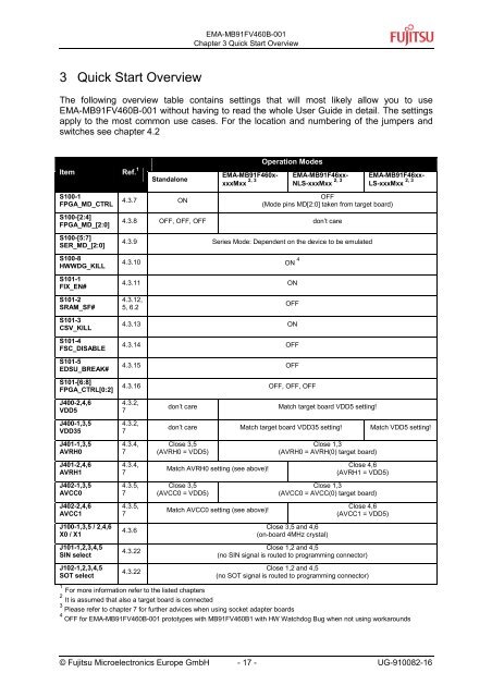
3 Quick Start Overview<br />
<strong>EMA</strong>-<strong>MB91FV460B</strong>-<strong>001</strong><br />
Chapter 3 Quick Start Overview<br />
The following overview table contains settings that will most likely allow you to use<br />
<strong>EMA</strong>-<strong>MB91FV460B</strong>-<strong>001</strong> without having to read the whole User Guide in detail. The settings<br />
apply to the most common use cases. For the location and numbering of the jumpers and<br />
switches see chapter 4.2<br />
Item Ref. 1<br />
S100-1<br />
FPGA_MD_CTRL<br />
S100-[2:4]<br />
FPGA_MD_[2:0]<br />
S100-[5:7]<br />
SER_MD_[2:0]<br />
S100-8<br />
HWWDG_KILL<br />
S101-1<br />
FIX_EN#<br />
S101-2<br />
SRAM_SF#<br />
S101-3<br />
CSV_KILL<br />
S101-4<br />
FSC_DISABLE<br />
S101-5<br />
EDSU_BREAK#<br />
S101-[6:8]<br />
FPGA_CTRL[0:2]<br />
J400-2,4,6<br />
VDD5<br />
J400-1,3,5<br />
VDD35<br />
J401-1,3,5<br />
AVRH0<br />
J401-2,4,6<br />
AVRH1<br />
J402-1,3,5<br />
AVCC0<br />
J402-2,4,6<br />
AVCC1<br />
J100-1,3,5 / 2,4,6<br />
X0 / X1<br />
J101-1,2,3,4,5<br />
SIN select<br />
J102-1,2,3,4,5<br />
SOT select<br />
Standalone<br />
4.3.7 ON<br />
<strong>EMA</strong>-MB91F460x-<br />
2, 3<br />
xxxMxx<br />
Operation Modes<br />
<strong>EMA</strong>-MB91F46xx-<br />
2, 3<br />
NLS-xxxMxx<br />
OFF<br />
(Mode pins MD[2:0] taken from target board)<br />
4.3.8 OFF, OFF, OFF don’t care<br />
4.3.9 Series Mode: Dependent on the device to be emulated<br />
4.3.10 ON 4<br />
4.3.11 ON<br />
4.3.12,<br />
5, 6.2<br />
<strong>EMA</strong>-MB91F46xx-<br />
2, 3<br />
LS-xxxMxx<br />
© <strong>Fujitsu</strong> Microelectronics Europe GmbH - 17 - UG-910082-16<br />
OFF<br />
4.3.13 ON<br />
4.3.14 OFF<br />
4.3.15 OFF<br />
4.3.16 OFF, OFF, OFF<br />
4.3.2,<br />
7<br />
4.3.2,<br />
7<br />
4.3.4,<br />
7<br />
4.3.4,<br />
7<br />
4.3.5,<br />
7<br />
4.3.5,<br />
7<br />
4.3.6<br />
4.3.22<br />
4.3.22<br />
don’t care Match target board VDD5 setting!<br />
don’t care Match target board VDD35 setting! Match VDD5 setting!<br />
Close 3,5<br />
(AVRH0 = VDD5)<br />
Match AVRH0 setting (see above)!<br />
Close 3,5<br />
(AVCC0 = VDD5)<br />
Match AVCC0 setting (see above)!<br />
Close 1,3<br />
(AVRH0 = AVRH(0) target board)<br />
Close 4,6<br />
(AVRH1 = VDD5)<br />
Close 1,3<br />
(AVCC0 = AVCC(0) target board)<br />
Close 3,5 and 4,6<br />
(on-board 4MHz crystal)<br />
Close 4,6<br />
(AVCC1 = VDD5)<br />
Close 1,2 and 4,5<br />
(no SIN signal is routed to programming connector)<br />
Close 1,2 and 4,5<br />
(no SOT signal is routed to programming connector)<br />
1 For more information refer to the listed chapters<br />
2 It is assumed that also a target board is connected<br />
3 Please refer to chapter 7 for further advices when using socket adapter boards<br />
4 OFF for <strong>EMA</strong>-<strong>MB91FV460B</strong>-<strong>001</strong> prototypes with <strong>MB91FV460B</strong>1 with HW Watchdog Bug when not using workarounds