LM13700 Dual Operational Transconductance ... - MIT Media Lab
LM13700 Dual Operational Transconductance ... - MIT Media Lab
LM13700 Dual Operational Transconductance ... - MIT Media Lab

Create successful ePaper yourself
Turn your PDF publications into a flip-book with our unique Google optimized e-Paper software.
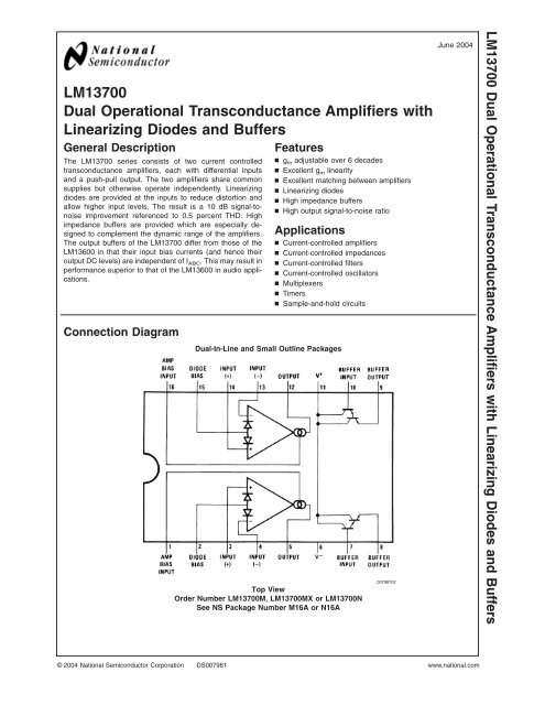
<strong>LM13700</strong><br />
<strong>Dual</strong> <strong>Operational</strong> <strong>Transconductance</strong> Amplifiers with<br />
Linearizing Diodes and Buffers<br />
General Description<br />
The <strong>LM13700</strong> series consists of two current controlled<br />
transconductance amplifiers, each with differential inputs<br />
and a push-pull output. The two amplifiers share common<br />
supplies but otherwise operate independently. Linearizing<br />
diodes are provided at the inputs to reduce distortion and<br />
allow higher input levels. The result is a 10 dB signal-tonoise<br />
improvement referenced to 0.5 percent THD. High<br />
impedance buffers are provided which are especially designed<br />
to complement the dynamic range of the amplifiers.<br />
The output buffers of the <strong>LM13700</strong> differ from those of the<br />
LM13600 in that their input bias currents (and hence their<br />
output DC levels) are independent of I ABC. This may result in<br />
performance superior to that of the LM13600 in audio applications.<br />
Connection Diagram<br />
Features<br />
n g m adjustable over 6 decades<br />
n Excellent g m linearity<br />
n Excellent matching between amplifiers<br />
n Linearizing diodes<br />
n High impedance buffers<br />
n High output signal-to-noise ratio<br />
Applications<br />
n Current-controlled amplifiers<br />
n Current-controlled impedances<br />
n Current-controlled filters<br />
n Current-controlled oscillators<br />
n Multiplexers<br />
n Timers<br />
n Sample-and-hold circuits<br />
<strong>Dual</strong>-In-Line and Small Outline Packages<br />
Top View<br />
Order Number <strong>LM13700</strong>M, <strong>LM13700</strong>MX or <strong>LM13700</strong>N<br />
See NS Package Number M16A or N16A<br />
00798102<br />
June 2004<br />
© 2004 National Semiconductor Corporation DS007981 www.national.com<br />
<strong>LM13700</strong> <strong>Dual</strong> <strong>Operational</strong> <strong>Transconductance</strong> Amplifiers with Linearizing Diodes and Buffers
<strong>LM13700</strong><br />
Absolute Maximum Ratings (Note 1)<br />
If Military/Aerospace specified devices are required,<br />
please contact the National Semiconductor Sales Office/<br />
Distributors for availability and specifications.<br />
Supply Voltage<br />
<strong>LM13700</strong><br />
Power Dissipation (Note 2) TA = 25˚C<br />
36 VDC or ±18V<br />
<strong>LM13700</strong>N 570 mW<br />
Differential Input Voltage ±5V<br />
Diode Bias Current (ID) 2 mA<br />
Amplifier Bias Current (IABC) 2 mA<br />
Output Short Circuit Duration Continuous<br />
Electrical Characteristics (Note 4)<br />
Buffer Output Current (Note 3)<br />
Operating Temperature Range<br />
20 mA<br />
<strong>LM13700</strong>N 0˚C to +70˚C<br />
DC Input Voltage +VS to −VS Storage Temperature Range<br />
Soldering Information<br />
<strong>Dual</strong>-In-Line Package<br />
−65˚C to +150˚C<br />
Soldering (10 sec.)<br />
Small Outline Package<br />
260˚C<br />
Vapor Phase (60 sec.) 215˚C<br />
Infrared (15 sec.) 220˚C<br />
Parameter Conditions<br />
Min<br />
<strong>LM13700</strong><br />
Typ Max<br />
Units<br />
Input Offset Voltage (VOS) Over Specified Temperature Range<br />
IABC = 5 µA<br />
0.4<br />
0.3<br />
4<br />
4<br />
mV<br />
VOS Including Diodes Diode Bias Current (ID) = 500 µA 0.5 5 mV<br />
Input Offset Change 5 µA ≤ IABC ≤ 500 µA 0.1 3 mV<br />
Input Offset Current 0.1 0.6 µA<br />
Input Bias Current Over Specified Temperature Range 0.4 5 µA<br />
1 8<br />
Forward 6700 9600 13000 µmho<br />
<strong>Transconductance</strong> (gm) Over Specified Temperature Range 5400<br />
gm Tracking 0.3 dB<br />
Peak Output Current RL =0,IABC =5µA 5<br />
RL =0,IABC = 500 µA 350 500 650 µA<br />
Peak Output Voltage<br />
RL = 0, Over Specified Temp Range 300<br />
Positive RL = ∞, 5µA≤ IABC ≤ 500 µA +12 +14.2 V<br />
Negative RL = ∞, 5µA≤ IABC ≤ 500 µA −12 −14.4 V<br />
Supply Current<br />
VOS Sensitivity<br />
IABC = 500 µA, Both Channels 2.6 mA<br />
Positive ∆VOS/∆V + 20 150 µV/V<br />
Negative ∆VOS/∆V− 20 150 µV/V<br />
CMRR 80 110 dB<br />
Common Mode Range ±12 ±13.5 V<br />
Crosstalk Referred to Input (Note 5)<br />
20 Hz < f < 20 kHz<br />
100 dB<br />
Differential Input Current IABC = 0, Input = ±4V 0.02 100 nA<br />
Leakage Current IABC = 0 (Refer to Test Circuit) 0.2 100 nA<br />
Input Resistance 10 26 kΩ<br />
Open Loop Bandwidth 2 MHz<br />
Slew Rate Unity Gain Compensated 50 V/µs<br />
Buffer Input Current (Note 5) 0.5 2 µA<br />
Peak Buffer Output Voltage (Note 5) 10 V<br />
Note 1: “Absolute Maximum Ratings” indicate limits beyond which damage to the device may occur. Operating Ratings indicate conditions for which the device is<br />
functional, but do not guarantee specific performance limits.<br />
Note 2: For operation at ambient temperatures above 25˚C, the device must be derated based on a 150˚C maximum junction temperature and a thermal resistance,<br />
junction to ambient, as follows: <strong>LM13700</strong>N, 90˚C/W; <strong>LM13700</strong>M, 110˚C/W.<br />
Note 3: Buffer output current should be limited so as to not exceed package dissipation.<br />
www.national.com 2
Electrical Characteristics (Note 4) (Continued)<br />
Note 4: These specifications apply for VS = ±15V, TA = 25˚C, amplifier bias current (IABC) = 500 µA, pins 2 and 15 open unless otherwise specified. The inputs to<br />
the buffers are grounded and outputs are open.<br />
Note 5: These specifications apply for VS = ±15V, IABC = 500 µA, ROUT =5kΩ connected from the buffer output to −VS and the input of the buffer is connected<br />
to the transconductance amplifier output.<br />
Schematic Diagram<br />
Typical Application<br />
One <strong>Operational</strong> <strong>Transconductance</strong> Amplifier<br />
Voltage Controlled Low-Pass Filter<br />
3<br />
00798118<br />
00798101<br />
www.national.com<br />
<strong>LM13700</strong>
<strong>LM13700</strong><br />
Typical Performance Characteristics<br />
Input Offset Voltage Input Offset Current<br />
00798138<br />
Input Bias Current Peak Output Current<br />
00798140<br />
Peak Output Voltage and<br />
Common Mode Range Leakage Current<br />
00798142<br />
www.national.com 4<br />
00798139<br />
00798141<br />
00798143
Typical Performance Characteristics (Continued)<br />
Input Leakage <strong>Transconductance</strong><br />
Input Resistance<br />
00798144 00798145<br />
00798146<br />
Amplifier Bias Voltage vs.<br />
Amplifier Bias Current<br />
Input and Output Capacitance Output Resistance<br />
00798147<br />
00798148 00798149<br />
5<br />
www.national.com<br />
<strong>LM13700</strong>
<strong>LM13700</strong><br />
Typical Performance Characteristics (Continued)<br />
Distortion vs. Differential<br />
Input Voltage<br />
Output Noise vs. Frequency<br />
00798150<br />
00798152<br />
Unity Gain Follower<br />
www.national.com 6<br />
Voltage vs. Amplifier<br />
Bias Current<br />
00798105<br />
00798151
Typical Performance Characteristics (Continued)<br />
Leakage Current Test Circuit Differential Input Current Test Circuit<br />
Circuit Description<br />
00798106<br />
The differential transistor pair Q 4 and Q 5 form a transconductance<br />
stage in that the ratio of their collector currents is<br />
defined by the differential input voltage according to the<br />
transfer function:<br />
(1)<br />
where VIN is the differential input voltage, kT/q is approximately<br />
26 mV at 25˚C and I5 and I4 are the collector currents<br />
of transistors Q5 and Q4 respectively. With the exception of<br />
Q12 and Q13, all transistors and diodes are identical in size.<br />
Transistors Q1 and Q2 with Diode D1 form a current mirror<br />
which forces the sum of currents I4 and I5 to equal IABC: I4 +I5 =IABC (2)<br />
where IABC is the amplifier bias current applied to the gain<br />
pin.<br />
For small differential input voltages the ratio of I4 and I5 approaches unity and the Taylor series of the In function can<br />
be approximated as:<br />
(4)<br />
Collector currents I4 and I5 are not very useful by themselves<br />
and it is necessary to subtract one current from the other.<br />
The remaining transistors and diodes form three current<br />
mirrors that produce an output current equal to I5 minus I4 thus:<br />
(5)<br />
The term in brackets is then the transconductance of the<br />
amplifier and is proportional to IABC. (3)<br />
7<br />
Linearizing Diodes<br />
00798107<br />
For differential voltages greater than a few millivolts, Equation<br />
(3) becomes less valid and the transconductance becomes<br />
increasingly nonlinear. Figure 1 demonstrates how<br />
the internal diodes can linearize the transfer function of the<br />
amplifier. For convenience assume the diodes are biased<br />
with current sources and the input signal is in the form of<br />
current I S. Since the sum of I 4 and I 5 is I ABC and the difference<br />
is I OUT, currents I 4 and I 5 can be written as follows:<br />
Since the diodes and the input transistors have identical<br />
geometries and are subject to similar voltages and temperatures,<br />
the following is true:<br />
(6)<br />
Notice that in deriving Equation (6) no approximations have<br />
been made and there are no temperature-dependent terms.<br />
The limitations are that the signal current not exceed ID/2 and that the diodes be biased with currents. In practice,<br />
replacing the current sources with resistors will generate<br />
insignificant errors.<br />
Applications<br />
Voltage Controlled Amplifiers<br />
Figure 2 shows how the linearizing diodes can be used in a<br />
voltage-controlled amplifier. To understand the input biasing,<br />
it is best to consider the 13 kΩ resistor as a current source<br />
and use a Thevenin equivalent circuit as shown in Figure 3.<br />
This circuit is similar to Figure 1 and operates the same. The<br />
potentiometer in Figure 2 is adjusted to minimize the effects<br />
of the control signal at the output.<br />
www.national.com<br />
<strong>LM13700</strong>
<strong>LM13700</strong><br />
Applications<br />
Voltage Controlled Amplifiers (Continued)<br />
For optimum signal-to-noise performance, I ABC should be as<br />
large as possible as shown by the Output Voltage vs. Amplifier<br />
Bias Current graph. Larger amplitudes of input signal<br />
also improve the S/N ratio. The linearizing diodes help here<br />
by allowing larger input signals for the same output distortion<br />
as shown by the Distortion vs. Differential Input Voltage<br />
graph. S/N may be optimized by adjusting the magnitude of<br />
the input signal via R IN (Figure 2) until the output distortion is<br />
below some desired level. The output voltage swing can<br />
then be set at any level by selecting R L.<br />
FIGURE 1. Linearizing Diodes<br />
FIGURE 2. Voltage Controlled Amplifier<br />
www.national.com 8<br />
00798108<br />
Although the noise contribution of the linearizing diodes is<br />
negligible relative to the contribution of the amplifier’s internal<br />
transistors, I D should be as large as possible. This minimizes<br />
the dynamic junction resistance of the diodes (r e) and<br />
maximizes their linearizing action when balanced against<br />
R IN. A value of 1 mA is recommended for I D unless the<br />
specific application demands otherwise.<br />
00798109
Applications<br />
Voltage Controlled Amplifiers (Continued)<br />
Stereo Volume Control<br />
The circuit of Figure 4 uses the excellent matching of the two<br />
<strong>LM13700</strong> amplifiers to provide a Stereo Volume Control with<br />
a typical channel-to-channel gain tracking of 0.3 dB. R P is<br />
provided to minimize the output offset voltage and may be<br />
replaced with two 510Ω resistors in AC-coupled applications.<br />
For the component values given, amplifier gain is derived for<br />
Figure 2 as being:<br />
FIGURE 3. Equivalent VCA Input Circuit<br />
9<br />
00798110<br />
If V C is derived from a second signal source then the circuit<br />
becomes an amplitude modulator or two-quadrant multiplier<br />
as shown in Figure 5, where:<br />
The constant term in the above equation may be cancelled<br />
by feeding I S xI DR C/2(V− + 1.4V) into I O. The circuit of<br />
Figure 6 adds R M to provide this current, resulting in a<br />
four-quadrant multiplier where R C is trimmed such that V O =<br />
0V for V IN2 =0V.R M also serves as the load resistor for I O.<br />
www.national.com<br />
<strong>LM13700</strong>
<strong>LM13700</strong><br />
Stereo Volume Control (Continued)<br />
FIGURE 4. Stereo Volume Control<br />
FIGURE 5. Amplitude Modulator<br />
www.national.com 10<br />
00798111<br />
00798112
Stereo Volume Control (Continued)<br />
Noting that the gain of the <strong>LM13700</strong> amplifier of Figure 3<br />
may be controlled by varying the linearizing diode current I D<br />
as well as by varying I ABC, Figure 7 shows an AGC Amplifier<br />
using this approach. As V O reaches a high enough amplitude<br />
(3V BE) to turn on the Darlington transistors and the linearizing<br />
diodes, the increase in I D reduces the amplifier gain so<br />
as to hold V O at that level.<br />
Voltage Controlled Resistors<br />
An <strong>Operational</strong> <strong>Transconductance</strong> Amplifier (OTA) may be<br />
used to implement a Voltage Controlled Resistor as shown in<br />
Figure 8. A signal voltage applied at R X generates a V IN to<br />
the <strong>LM13700</strong> which is then multiplied by the g m of the<br />
amplifier to produce an output current, thus:<br />
FIGURE 6. Four-Quadrant Multiplier<br />
FIGURE 7. AGC Amplifier<br />
11<br />
00798113<br />
where gm ≈ 19.2IABC at 25˚C. Note that the attenuation of VO by R and RA is necessary to maintain VIN within the linear<br />
range of the <strong>LM13700</strong> input.<br />
Figure 9 shows a similar VCR where the linearizing diodes<br />
are added, essentially improving the noise performance of<br />
the resistor. A floating VCR is shown in Figure 10, where<br />
each “end” of the “resistor” may be at any voltage within the<br />
output voltage range of the <strong>LM13700</strong>.<br />
00798114<br />
www.national.com<br />
<strong>LM13700</strong>
<strong>LM13700</strong><br />
Voltage Controlled Resistors (Continued)<br />
Voltage Controlled Filters<br />
OTA’s are extremely useful for implementing voltage controlled<br />
filters, with the <strong>LM13700</strong> having the advantage that<br />
the required buffers are included on the I.C. The VC Lo-Pass<br />
Filter of Figure 11 performs as a unity-gain buffer amplifier at<br />
frequencies below cut-off, with the cut-off frequency being<br />
the point at which X C/g m equals the closed-loop gain of<br />
(R/R A). At frequencies above cut-off the circuit provides a<br />
single RC roll-off (6 dB per octave) of the input signal amplitude<br />
with a −3 dB point defined by the given equation, where<br />
FIGURE 8. Voltage Controlled Resistor, Single-Ended<br />
FIGURE 9. Voltage Controlled Resistor with Linearizing Diodes<br />
www.national.com 12<br />
00798115<br />
00798116<br />
gm is again 19.2 x IABC at room temperature. Figure 12<br />
shows a VC High-Pass Filter which operates in much the<br />
same manner, providing a single RC roll-off below the defined<br />
cut-off frequency.<br />
Additional amplifiers may be used to implement higher order<br />
filters as demonstrated by the two-pole Butterworth Lo-Pass<br />
Filter of Figure 13 and the state variable filter of Figure 14.<br />
Due to the excellent gm tracking of the two amplifiers, these<br />
filters perform well over several decades of frequency.
Voltage Controlled Filters (Continued)<br />
FIGURE 10. Floating Voltage Controlled Resistor<br />
FIGURE 11. Voltage Controlled Low-Pass Filter<br />
13<br />
00798118<br />
00798117<br />
www.national.com<br />
<strong>LM13700</strong>
<strong>LM13700</strong><br />
Voltage Controlled Filters (Continued)<br />
FIGURE 12. Voltage Controlled Hi-Pass Filter<br />
FIGURE 13. Voltage Controlled 2-Pole Butterworth Lo-Pass Filter<br />
www.national.com 14<br />
00798119<br />
00798120
Voltage Controlled Filters (Continued)<br />
Voltage Controlled Oscillators<br />
The classic Triangular/Square Wave VCO of Figure 15 is<br />
one of a variety of Voltage Controlled Oscillators which may<br />
be built utilizing the <strong>LM13700</strong>. With the component values<br />
shown, this oscillator provides signals from 200 kHz to below<br />
2 Hz as IC is varied from 1 mA to 10 nA. The output<br />
amplitudes are set by IA xRA. Note that the peak differential<br />
input voltage must be less than 5V to prevent zenering the<br />
inputs.<br />
A few modifications to this circuit produce the ramp/pulse<br />
VCO of Figure 16. When VO2 is high, IF is added to IC to<br />
FIGURE 14. Voltage Controlled State Variable Filter<br />
15<br />
00798121<br />
increase amplifier A1’s bias current and thus to increase the<br />
charging rate of capacitor C. When VO2 is low, IF goes to<br />
zero and the capacitor discharge current is set by IC. The VC Lo-Pass Filter of Figure 11 may be used to produce<br />
a high-quality sinusoidal VCO. The circuit of Figure 16 employs<br />
two <strong>LM13700</strong> packages, with three of the amplifiers<br />
configured as lo-pass filters and the fourth as a limiter/<br />
inverter. The circuit oscillates at the frequency at which the<br />
loop phase-shift is 360˚ or 180˚ for the inverter and 60˚ per<br />
filter stage. This VCO operates from 5 Hz to 50 kHz with less<br />
than 1% THD.<br />
www.national.com<br />
<strong>LM13700</strong>
<strong>LM13700</strong><br />
Voltage Controlled Oscillators (Continued)<br />
FIGURE 15. Triangular/Square-Wave VCO<br />
FIGURE 16. Ramp/Pulse VCO<br />
www.national.com 16<br />
00798122<br />
00798123
Voltage Controlled Oscillators (Continued)<br />
00798125<br />
Figure 18 shows how to build a VCO using one amplifier when the other<br />
amplifier is needed for another function.<br />
FIGURE 18. Single Amplifier VCO<br />
FIGURE 17. Sinusoidal VCO<br />
17<br />
Additional Applications<br />
00798124<br />
Figure 19 presents an interesting one-shot which draws no<br />
power supply current until it is triggered. A positive-going<br />
trigger pulse of at least 2V amplitude turns on the amplifier<br />
through R B and pulls the non-inverting input high. The amplifier<br />
regenerates and latches its output high until capacitor<br />
C charges to the voltage level on the non-inverting input. The<br />
output then switches low, turning off the amplifier and discharging<br />
the capacitor. The capacitor discharge rate is<br />
speeded up by shorting the diode bias pin to the inverting<br />
input so that an additional discharge current flows through D I<br />
when the amplifier output switches low. A special feature of<br />
this timer is that the other amplifier, when biased from V O,<br />
can perform another function and draw zero stand-by power<br />
as well.<br />
www.national.com<br />
<strong>LM13700</strong>
<strong>LM13700</strong><br />
Additional Applications (Continued)<br />
The operation of the multiplexer of Figure 20 is very straightforward.<br />
When A1 is turned on it holds V O equal to V IN1 and<br />
when A2 is supplied with bias current then it controls V O.C C<br />
and R C serve to stabilize the unity-gain configuration of<br />
amplifiers A1 and A2. The maximum clock rate is limited to<br />
about 200 kHz by the <strong>LM13700</strong> slew rate into 150 pF when<br />
the (V IN1–V IN2) differential is at its maximum allowable value<br />
of 5V.<br />
FIGURE 19. Zero Stand-By Power Timer<br />
FIGURE 20. Multiplexer<br />
www.national.com 18<br />
00798126<br />
The Phase-Locked Loop of Figure 21 uses the four-quadrant<br />
multiplier of Figure 6 and the VCO of Figure 18 to produce a<br />
PLL with a ±5% hold-in range and an input sensitivity of<br />
about 300 mV.<br />
00798127
Additional Applications (Continued)<br />
The Schmitt Trigger of Figure 22 uses the amplifier output<br />
current into R to set the hysteresis of the comparator; thus<br />
V H =2xRxI B. Varying I B will produce a Schmitt Trigger with<br />
variable hysteresis.<br />
Figure 23 shows a Tachometer or Frequency-to-Voltage converter.<br />
Whenever A1 is toggled by a positive-going input, an<br />
amount of charge equal to (V H–V L)C t is sourced into C f and<br />
R t. This once per cycle charge is then balanced by the<br />
current of V O/R t. The maximum F IN is limited by the amount<br />
of time required to charge C t from V L to V H with a current of<br />
I B, where V L and V H represent the maximum low and maximum<br />
high output voltage swing of the <strong>LM13700</strong>. D1 is added<br />
to provide a discharge path for C t when A1 switches low.<br />
FIGURE 21. Phase Lock Loop<br />
FIGURE 22. Schmitt Trigger<br />
19<br />
00798129<br />
00798128<br />
The Peak Detector of Figure 24 uses A2 to turn on A1<br />
whenever V IN becomes more positive than V O. A1 then<br />
charges storage capacitor C to hold V O equal to V IN PK.<br />
Pulling the output of A2 low through D1 serves to turn off A1<br />
so that V O remains constant.<br />
www.national.com<br />
<strong>LM13700</strong>
<strong>LM13700</strong><br />
Additional Applications (Continued)<br />
The Ramp-and-Hold of Figure 26 sources IB into capacitor C<br />
whenever the input to A1 is brought high, giving a ramp-rate<br />
of about 1V/ms for the component values shown.<br />
The true-RMS converter of Figure 27 is essentially an automatic<br />
gain control amplifier which adjusts its gain such that<br />
the AC power at the output of amplifier A1 is constant. The<br />
output power of amplifier A1 is monitored by squaring amplifier<br />
A2 and the average compared to a reference voltage<br />
with amplifier A3. The output of A3 provides bias current to<br />
FIGURE 23. Tachometer<br />
FIGURE 24. Peak Detector and Hold Circuit<br />
www.national.com 20<br />
00798130<br />
00798131<br />
the diodes of A1 to attenuate the input signal. Because the<br />
output power of A1 is held constant, the RMS value is<br />
constant and the attenuation is directly proportional to the<br />
RMS value of the input voltage. The attenuation is also<br />
proportional to the diode bias current. Amplifier A4 adjusts<br />
the ratio of currents through the diodes to be equal and<br />
therefore the voltage at the output of A4 is proportional to the<br />
RMS value of the input voltage. The calibration potentiometer<br />
is set such that V O reads directly in RMS volts.
Additional Applications (Continued)<br />
FIGURE 25. Sample-Hold Circuit<br />
FIGURE 26. Ramp and Hold<br />
21<br />
00798132<br />
00798133<br />
www.national.com<br />
<strong>LM13700</strong>
<strong>LM13700</strong><br />
Additional Applications (Continued)<br />
The circuit of Figure 28 is a voltage reference of variable<br />
Temperature Coefficient. The 100 kΩ potentiometer adjusts<br />
the output voltage which has a positive TC above 1.2V, zero<br />
TC at about 1.2V, and negative TC below 1.2V. This is<br />
accomplished by balancing the TC of the A2 transfer function<br />
against the complementary TC of D1.<br />
The wide dynamic range of the <strong>LM13700</strong> allows easy control<br />
of the output pulse width in the Pulse Width Modulator of<br />
Figure 29.<br />
For generating IABC over a range of 4 to 6 decades of<br />
current, the system of Figure 30 provides a logarithmic current<br />
out for a linear voltage in.<br />
Since the closed-loop configuration ensures that the input to<br />
A2 is held equal to 0V, the output current of A1 is equal to<br />
I3 =−VC/RC. The differential voltage between Q1 and Q2 is attenuated by<br />
the R1,R2 network so that A1 may be assumed to be operating<br />
within its linear range. From Equation (5), the input<br />
voltage to A1 is:<br />
FIGURE 27. True RMS Converter<br />
www.national.com 22<br />
The voltage on the base of Q1 is then<br />
The ratio of the Q1 and Q2 collector currents is defined by:<br />
Combining and solving for I ABC yields:<br />
00798134<br />
This logarithmic current can be used to bias the circuit of<br />
Figure 4 to provide temperature independent stereo attenuation<br />
characteristic.
Additional Applications (Continued)<br />
FIGURE 28. Delta VBE Reference<br />
FIGURE 29. Pulse Width Modulator<br />
23<br />
00798135<br />
00798136<br />
www.national.com<br />
<strong>LM13700</strong>
<strong>LM13700</strong><br />
Additional Applications (Continued)<br />
FIGURE 30. Logarithmic Current Source<br />
www.national.com 24<br />
00798137
Physical Dimensions inches (millimeters) unless otherwise noted<br />
S.O. Package (M)<br />
Order Number <strong>LM13700</strong>M or <strong>LM13700</strong>MX<br />
NS Package Number M16A<br />
Molded <strong>Dual</strong>-In-Line Package (N)<br />
Order Number <strong>LM13700</strong>N<br />
NS Package Number N16A<br />
25<br />
www.national.com<br />
<strong>LM13700</strong>
<strong>LM13700</strong> <strong>Dual</strong> <strong>Operational</strong> <strong>Transconductance</strong> Amplifiers with Linearizing Diodes and Buffers<br />
LIFE SUPPORT POLICY<br />
Notes<br />
NATIONAL’S PRODUCTS ARE NOT AUTHORIZED FOR USE AS CRITICAL COMPONENTS IN LIFE SUPPORT<br />
DEVICES OR SYSTEMS WITHOUT THE EXPRESS WRITTEN APPROVAL OF THE PRESIDENT AND GENERAL<br />
COUNSEL OF NATIONAL SEMICONDUCTOR CORPORATION. As used herein:<br />
1. Life support devices or systems are devices or<br />
systems which, (a) are intended for surgical implant<br />
into the body, or (b) support or sustain life, and<br />
whose failure to perform when properly used in<br />
accordance with instructions for use provided in the<br />
labeling, can be reasonably expected to result in a<br />
significant injury to the user.<br />
BANNED SUBSTANCE COMPLIANCE<br />
2. A critical component is any component of a life<br />
support device or system whose failure to perform<br />
can be reasonably expected to cause the failure of<br />
the life support device or system, or to affect its<br />
safety or effectiveness.<br />
National Semiconductor certifies that the products and packing materials meet the provisions of the Customer Products<br />
Stewardship Specification (CSP-9-111C2) and the Banned Substances and Materials of Interest Specification<br />
(CSP-9-111S2) and contain no ‘‘Banned Substances’’ as defined in CSP-9-111S2.<br />
National Semiconductor<br />
Americas Customer<br />
Support Center<br />
Email: new.feedback@nsc.com<br />
Tel: 1-800-272-9959<br />
www.national.com<br />
National Semiconductor<br />
Europe Customer Support Center<br />
Fax: +49 (0) 180-530 85 86<br />
Email: europe.support@nsc.com<br />
Deutsch Tel: +49 (0) 69 9508 6208<br />
English Tel: +44 (0) 870 24 0 2171<br />
Français Tel: +33 (0) 1 41 91 8790<br />
National Semiconductor<br />
Asia Pacific Customer<br />
Support Center<br />
Email: ap.support@nsc.com<br />
National Semiconductor<br />
Japan Customer Support Center<br />
Fax: 81-3-5639-7507<br />
Email: jpn.feedback@nsc.com<br />
Tel: 81-3-5639-7560<br />
National does not assume any responsibility for use of any circuitry described, no circuit patent licenses are implied and National reserves the right at any time without notice to change said circuitry and specifications.