datasheet: pdf - svn
datasheet: pdf - svn
datasheet: pdf - svn

Create successful ePaper yourself
Turn your PDF publications into a flip-book with our unique Google optimized e-Paper software.
1. General description<br />
2. Features<br />
3. Ordering information<br />
Table 1. Ordering information<br />
All types operate from −40 °C to +125 °C.<br />
Type number Package<br />
HEF4094B<br />
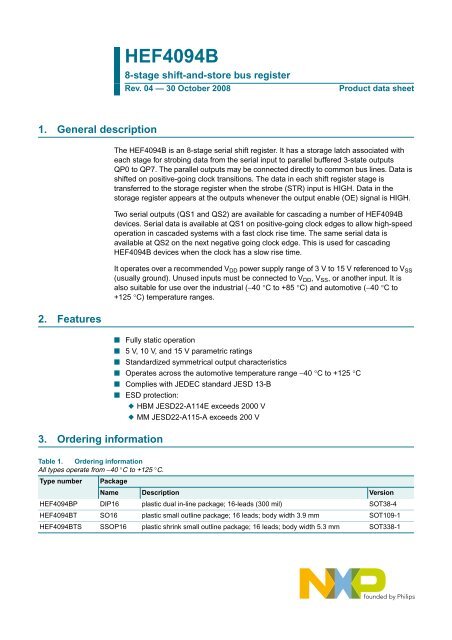
8-stage shift-and-store bus register<br />
Rev. 04 — 30 October 2008 Product data sheet<br />
The HEF4094B is an 8-stage serial shift register. It has a storage latch associated with<br />
each stage for strobing data from the serial input to parallel buffered 3-state outputs<br />
QP0 to QP7. The parallel outputs may be connected directly to common bus lines. Data is<br />
shifted on positive-going clock transitions. The data in each shift register stage is<br />
transferred to the storage register when the strobe (STR) input is HIGH. Data in the<br />
storage register appears at the outputs whenever the output enable (OE) signal is HIGH.<br />
Two serial outputs (QS1 and QS2) are available for cascading a number of HEF4094B<br />
devices. Serial data is available at QS1 on positive-going clock edges to allow high-speed<br />
operation in cascaded systems with a fast clock rise time. The same serial data is<br />
available at QS2 on the next negative going clock edge. This is used for cascading<br />
HEF4094B devices when the clock has a slow rise time.<br />
It operates over a recommended VDD power supply range of 3 V to 15 V referenced to VSS<br />
(usually ground). Unused inputs must be connected to VDD, VSS, or another input. It is<br />
also suitable for use over the industrial (−40 °C to +85 °C) and automotive (−40 °C to<br />
+125 °C) temperature ranges.<br />
■ Fully static operation<br />
■ 5 V, 10 V, and 15 V parametric ratings<br />
■ Standardized symmetrical output characteristics<br />
■ Operates across the automotive temperature range −40 °C to +125 °C<br />
■ Complies with JEDEC standard JESD 13-B<br />
■ ESD protection:<br />
◆ HBM JESD22-A114E exceeds 2000 V<br />
◆ MM JESD22-A115-A exceeds 200 V<br />
Name Description Version<br />
HEF4094BP DIP16 plastic dual in-line package; 16-leads (300 mil) SOT38-4<br />
HEF4094BT SO16 plastic small outline package; 16 leads; body width 3.9 mm SOT109-1<br />
HEF4094BTS SSOP16 plastic shrink small outline package; 16 leads; body width 5.3 mm SOT338-1
NXP Semiconductors HEF4094B<br />
4. Functional diagram<br />
2<br />
3<br />
1<br />
15<br />
D<br />
CP<br />
STR<br />
OE<br />
QP0<br />
8-STAGE SHIFT<br />
REGISTER<br />
8-BIT STORAGE<br />
REGISTER<br />
3-STATE OUTPUTS<br />
4 5 6 7 14 13 12 11<br />
001aaf119<br />
Fig 1. Functional diagram Fig 2. Logic symbol<br />
D<br />
CP<br />
STR<br />
OE<br />
Fig 3. Logic diagram<br />
QS2<br />
QS1<br />
QP1 QP2 QP3 QP4 QP5 QP6 QP7<br />
10<br />
9<br />
STAGE 0 STAGES 1 TO 6<br />
STAGE 7<br />
D<br />
CP<br />
D<br />
CP<br />
FF 0<br />
Q<br />
Q<br />
LATCH 0<br />
QP0<br />
D<br />
CP<br />
8-stage shift-and-store bus register<br />
HEF4094B_4 © NXP B.V. 2008. All rights reserved.<br />
Product data sheet Rev. 04 — 30 October 2008 2 of 17<br />
D<br />
2<br />
CP<br />
D<br />
CP<br />
FF 7<br />
Q<br />
Q<br />
LATCH 7<br />
QP2 QP4 QP6<br />
QP1 QP3 QP5 QP7<br />
Q<br />
D<br />
3 1<br />
CP STR<br />
OE<br />
15<br />
QS1<br />
QS2<br />
QP0<br />
QP1<br />
QP2<br />
QP3<br />
QP4<br />
QP5<br />
QP6<br />
QP7<br />
001aag799<br />
9<br />
10<br />
4<br />
5<br />
6<br />
7<br />
14<br />
13<br />
12<br />
11<br />
001aaf111<br />
QS1<br />
D Q QS2<br />
CP<br />
LATCH
NXP Semiconductors HEF4094B<br />
5. Pinning information<br />
5.1 Pinning<br />
Fig 4. Pin configuration<br />
5.2 Pin description<br />
6. Functional description<br />
HEF4094B<br />
STR 1<br />
16 VDD<br />
D 2<br />
15 OE<br />
CP 3<br />
14 QP4<br />
QP0 4<br />
13 QP5<br />
QP1 5<br />
12 QP6<br />
QP2 6<br />
11 QP7<br />
QP3 7<br />
10 QS2<br />
VSS<br />
8<br />
001aae662<br />
Table 2. Pin description<br />
Symbol Pin Description<br />
STR 1 strobe input<br />
D 2 data input<br />
CP 3 clock input<br />
QP0 to QP7 4, 5, 6, 7, 14, 13, 12, 11 parallel output<br />
VSS 8 ground supply voltage<br />
QS1 9 serial output<br />
QS2 10 serial output<br />
OE 15 output enable input<br />
VDD 16 supply voltage<br />
8-stage shift-and-store bus register<br />
Table 3. Function table [1]<br />
Inputs Parallel outputs Serial outputs<br />
CP OE STR D QP0 QPn QS1 QS2<br />
↑ L X X Z Z Q6S NC<br />
↓ L X X Z Z NC Q7S<br />
↑ H L X NC NC QS6 NC<br />
↑ H H L L QPn −1 QS6 NC<br />
↑ H H H H QPn −1 QS6 NC<br />
HEF4094B_4 © NXP B.V. 2008. All rights reserved.<br />
Product data sheet Rev. 04 — 30 October 2008 3 of 17<br />
9<br />
QS1
NXP Semiconductors HEF4094B<br />
Table 3. Function table [1] …continued<br />
8-stage shift-and-store bus register<br />
Inputs Parallel outputs Serial outputs<br />
CP OE STR D QP0 QPn QS1 QS2<br />
↓ H H H NC NC NC Q7S<br />
[1] At the positive clock edge, the information in the 7th register stage is transferred to the 8th register stage and the QSn outputs.<br />
H = HIGH voltage level; L = LOW voltage level; X = don’t care;<br />
↑ = positive-going transition; ↓ = negative-going transition;<br />
Z = HIGH-impedance OFF-state; NC = no change;<br />
Q6S = the data in register stage 6 before the LOW to HIGH clock transition;<br />
Q7S = the data in register stage 7 before the HIGH to LOW clock transition.<br />
Fig 5. Timing diagram<br />
CLOCK INPUT<br />
DATA INPUT<br />
STROBE INPUT<br />
OUTPUT ENABLE INPUT<br />
INTERNAL Q0S (FF 0)<br />
OUTPUT QP0<br />
INTERNAL Q6S (FF 6)<br />
OUTPUT QP6<br />
SERIAL OUTPUT QS1<br />
SERIAL OUTPUT QS2<br />
7. Limiting values<br />
[1] For DIP16 packages: above Tamb = 70 °C, Ptot derates linearly with 12 mW/K.<br />
[2] For SO16 packages: above Tamb = 70 °C, Ptot derates linearly with 8 mW/K.<br />
001aaf117<br />
Table 4. Limiting values<br />
In accordance with the Absolute Maximum Rating System (IEC 60134). Voltages are referenced to VSS = 0 V (ground).<br />
Symbol Parameter Conditions Min Max Unit<br />
VDD supply voltage −0.5 +18 V<br />
IIK input clamping current VI < 0.5 V or VI >VDD + 0.5 V - ±10 mA<br />
VI input voltage −0.5 VDD + 0.5 V<br />
IOK output clamping current VO < 0.5 V or VO >VDD + 0.5 V - ±10 mA<br />
II/O input/output current - ±10 mA<br />
IDD supply current - 50 mA<br />
Tstg storage temperature −65 +150 °C<br />
Tamb ambient temperature −40 +125 °C<br />
Ptot total power dissipation DIP16 [1] - 750 mW<br />
SO16 [2] - 500 mW<br />
P power dissipation per output - 100 mW<br />
HEF4094B_4 © NXP B.V. 2008. All rights reserved.<br />
Product data sheet Rev. 04 — 30 October 2008 4 of 17<br />
Z-state<br />
Z-state
NXP Semiconductors HEF4094B<br />
8. Recommended operating conditions<br />
Table 5. Recommended operating conditions<br />
9. Static characteristics<br />
8-stage shift-and-store bus register<br />
Symbol Parameter Conditions Min Typ Max Unit<br />
VDD supply voltage 3 - 15 V<br />
VI input voltage 0 - VDD V<br />
Tamb ambient temperature in free air −40 - +125 °C<br />
Δt/ΔV input transition rise and fall rate VDD = 5 V - - 3.75 ns/V<br />
VDD = 10 V - - 0.5 ns/V<br />
VDD = 15 V - - 0.08 ns/V<br />
Table 6. Static characteristics<br />
VSS = 0 V; VI =VSS or VDD; unless otherwise specified.<br />
Symbol Parameter Conditions VDD Tamb = −40 °C Tamb = +25 °C Tamb = +85 °C Tamb = +125 °C Unit<br />
VIH<br />
VIL<br />
VOH<br />
VOL<br />
IOH<br />
IOL<br />
IOZ<br />
II<br />
HIGH-level<br />
input voltage<br />
LOW-level<br />
input voltage<br />
HIGH-level<br />
output voltage<br />
LOW-level<br />
output voltage<br />
HIGH-level<br />
output current<br />
LOW-level<br />
output current<br />
OFF-state<br />
output current<br />
input leakage<br />
current<br />
Min Max Min Max Min Max Min Max<br />
|IO| < 1 μA 5 V 3.5 - 3.5 - 3.5 - 3.5 - V<br />
10 V 7.0 - 7.0 - 7.0 - 7.0 - V<br />
15 V 11.0 - 11.0 - 11.0 - 11.0 - V<br />
|IO| < 1 μA 5 V - 1.5 - 1.5 - 1.5 - 1.5 V<br />
10 V - 3.0 - 3.0 - 3.0 - 3.0 V<br />
15 V - 4.0 - 4.0 - 4.0 - 4.0 V<br />
|IO| < 1 μA 5 V 4.95 - 4.95 - 4.95 - 4.95 - V<br />
10 V 9.95 - 9.95 - 9.95 - 9.95 - V<br />
15 V 14.95 - 14.95 - 14.95 - 14.95 - V<br />
|IO| < 1 μA 5 V - 0.05 - 0.05 - 0.05 - 0.05 V<br />
10 V - 0.05 - 0.05 - 0.05 - 0.05 V<br />
15 V - 0.05 - 0.05 - 0.05 - 0.05 V<br />
VO = 2.5 V 5 V −1.7 - −1.4 - −1.1 - −1.1 - mA<br />
VO = 4.6 V 5 V −0.64 - −0.5 - −0.36 - −0.36 - mA<br />
VO = 9.5 V 10 V −1.6 - −1.3 - −0.9 - −0.9 - mA<br />
VO = 13.5 V 15 V −4.2 - −3.4 - −2.4 - −2.4 - mA<br />
VO = 0.4 V 5 V 0.64 - 0.5 - 0.36 - 0.36 - mA<br />
VO = 0.5 V 10 V 1.6 - 1.3 - 0.9 - 0.9 - mA<br />
VO = 1.5 V 15 V 4.2 - 3.4 - 2.4 - 2.4 - mA<br />
QPn output<br />
is HIGH;<br />
VO =15V<br />
15 V - 0.4 - 0.4 - 12 - 12 μA<br />
15 V - ±0.1 - ±0.1 - ±1.0 - ±1.0 μA<br />
HEF4094B_4 © NXP B.V. 2008. All rights reserved.<br />
Product data sheet Rev. 04 — 30 October 2008 5 of 17
NXP Semiconductors HEF4094B<br />
Table 6. Static characteristics …continued<br />
VSS = 0 V; VI =VSS or VDD; unless otherwise specified.<br />
IDD supply current all valid input<br />
combinations;<br />
IO =0A<br />
CI<br />
input<br />
capacitance<br />
10. Dynamic characteristics<br />
8-stage shift-and-store bus register<br />
Symbol Parameter Conditions VDD Tamb = −40 °C Tamb = +25 °C Tamb = +85 °C Tamb = +125 °C Unit<br />
Table 7. Dynamic characteristics<br />
VSS = 0 V; Tamb = 25 °C; for test circuit see Figure 10; unless otherwise specified.<br />
Min Max Min Max Min Max Min Max<br />
5 V - 5 - 5 - 150 - 150 μA<br />
10 V - 10 - 10 - 300 - 300 μA<br />
15 V - 20 - 20 - 600 - 600 μA<br />
- - - 7.5 - - - - pF<br />
Symbol Parameter Conditions VDD Extrapolation formula Min Typ Max Unit<br />
tPHL<br />
tPLH<br />
HIGH to LOW<br />
propagation delay<br />
LOW to HIGH<br />
propagation delay,<br />
CP to QS1;<br />
see Figure 6<br />
CP to QS2;<br />
see Figure 6<br />
CP to QPn;<br />
see Figure 6<br />
STR to QPn;<br />
see Figure 7<br />
CP to QS1;<br />
see Figure 6<br />
CP to QS2;<br />
see Figure 6<br />
CP to QPn;<br />
see Figure 6<br />
5 V [1] 108 ns + (0.55 ns/pF) CL - 135 270 ns<br />
10 V 54 ns + (0.23 ns/pF) CL - 65 130 ns<br />
15 V 42 ns + (0.16 ns/pF) CL - 50 100 ns<br />
5 V 78 ns + (0.55 ns/pF) CL - 105 210 ns<br />
10 V 39 ns + (0.23 ns/pF) CL - 50 100 ns<br />
15 V 32 ns + (0.16 ns/pF) CL - 40 80 ns<br />
5 V 138 ns + (0.55 ns/pF) CL - 165 330 ns<br />
10 V 64 ns + (0.23 ns/pF) CL - 75 150 ns<br />
15 V 47 ns + (0.16 ns/pF) CL - 55 110 ns<br />
5 V 83 ns + (0.55 ns/pF) CL - 110 220 ns<br />
10 V 39 ns + (0.23 ns/pF) CL - 50 100 ns<br />
15 V 27 ns + (0.16 ns/pF) CL - 35 70 ns<br />
5 V [1] 78 ns + (0.55 ns/pF) CL - 105 210 ns<br />
10 V 39 ns + (0.23 ns/pF) CL - 50 100 ns<br />
15 V 32 ns + (0.16 ns/pF) CL - 40 80 ns<br />
5 V 78 ns + (0.55 ns/pF) CL - 105 210 ns<br />
10 V 39 ns + (0.23 ns/pF) CL - 50 100 ns<br />
15 V 32 ns + (0.16 ns/pF) CL - 40 80 ns<br />
5 V 123 ns + (0.55 ns/pF) CL - 150 300 ns<br />
10 V 59 ns + (0.23 ns/pF) CL - 70 140 ns<br />
15 V 47 ns + (0.16 ns/pF) CL - 55 110 ns<br />
STR to QPn; 5 V 73 ns + (0.55 ns/pF) CL - 100 200 ns<br />
see Figure 7<br />
10 V 34 ns + (0.23 ns/pF) CL - 45 90 ns<br />
15 V 27 ns + (0.16 ns/pF) CL - 35 70 ns<br />
tt transition time 5 V [1] 10 ns + (1.00 ns/pF) CL - 60 120 ns<br />
10 V 9 ns + (0.42 ns/pF) CL - 30 60 ns<br />
15 V 6 ns + (0.28 ns/pF) CL - 20 40 ns<br />
HEF4094B_4 © NXP B.V. 2008. All rights reserved.<br />
Product data sheet Rev. 04 — 30 October 2008 6 of 17
NXP Semiconductors HEF4094B<br />
Table 7. Dynamic characteristics …continued<br />
VSS = 0 V; Tamb = 25 °C; for test circuit see Figure 10; unless otherwise specified.<br />
tPZH<br />
tPZL<br />
tPHZ<br />
tPLZ<br />
OFF-state to HIGH<br />
propagation delay<br />
OFF-state to LOW<br />
propagation delay<br />
HIGH to OFF-state<br />
propagation delay<br />
LOW to OFF-state<br />
propagation delay<br />
OE to QPn;<br />
see Figure 8<br />
OE to QPn;<br />
see Figure 8<br />
OE to QPn;<br />
see Figure 8<br />
OE to QPn;<br />
see Figure 8<br />
tsu set-up time D to CP;<br />
see Figure 9<br />
th hold time D to CP;<br />
see Figure 9<br />
tW pulse width minimum LOW<br />
clock pulse;<br />
see Figure 6<br />
8-stage shift-and-store bus register<br />
Symbol Parameter Conditions VDD Extrapolation formula Min Typ Max Unit<br />
5 V - 40 80 MHz<br />
10 V - 25 50 MHz<br />
15 V - 20 40 MHz<br />
5 V - 40 80 MHz<br />
10 V - 25 50 MHz<br />
15 V - 20 40 MHz<br />
5 V - 75 150 MHz<br />
10 V - 40 80 MHz<br />
15 V - 30 60 MHz<br />
5 V - 80 160 MHz<br />
10 V - 40 80 MHz<br />
15 V - 30 60 MHz<br />
5 V 60 30 - ns<br />
10 V 20 10 - ns<br />
15 V 15 5 - ns<br />
5 V +5 −15 - ns<br />
10 V 20 5 - ns<br />
15 V 20 5 - ns<br />
5 V 60 30 - ns<br />
10 V 30 15 - ns<br />
15 V 24 12 - ns<br />
minimum HIGH 5 V 40 20 - ns<br />
strobe pulse;<br />
see Figure 7<br />
10 V<br />
15 V<br />
30<br />
24<br />
15<br />
12<br />
-<br />
-<br />
ns<br />
ns<br />
fmax maximum frequency see Figure 6 5 V 5 10 - MHz<br />
10 V 11 22 - MHz<br />
15 V 14 28 - MHz<br />
[1] The typical values of the propagation delay and transition times are calculated from the extrapolation formulas shown (CL in pF).<br />
Table 8. Dynamic power dissipation<br />
VSS = 0 V; tr = tf ≤ 20 ns; Tamb = 25 °C.<br />
Symbol Parameter VDD Typical formula for PD (μW) where:<br />
PD dynamic power 5 V PD = 2100 × fi + Σ(fo × CL) × VDD<br />
dissipation<br />
2 fi = input frequency in MHz,<br />
10 V PD = 9700 × fi + Σ(fo × CL) × VDD fo = output frequency in MHz,<br />
CL = output load capacitance in pF,<br />
VDD = supply voltage in V,<br />
Σ(CL × fo) = sum of the outputs.<br />
2<br />
15 V PD = 26000 × fi + Σ(fo × CL) × VDD 2<br />
HEF4094B_4 © NXP B.V. 2008. All rights reserved.<br />
Product data sheet Rev. 04 — 30 October 2008 7 of 17
NXP Semiconductors HEF4094B<br />
11. Waveforms<br />
Measurement points are given in Table 9.<br />
Logic levels: VOL and VOH are typical output voltage drops that occur with the output load.<br />
Fig 6. Clock to outputs propagation delays, and clock pulse width and maximum frequency<br />
Table 9. Measurement points<br />
VI<br />
CP input VM<br />
QPn, QS1 output<br />
GND<br />
VOH<br />
VOL<br />
VOH<br />
VOL<br />
tPLH<br />
tW<br />
1/fmax<br />
VM<br />
8-stage shift-and-store bus register<br />
HEF4094B_4 © NXP B.V. 2008. All rights reserved.<br />
Product data sheet Rev. 04 — 30 October 2008 8 of 17<br />
tPLH<br />
QS2 output VM<br />
Supply voltage Input Output<br />
tPHL<br />
tPHL<br />
001aaf113<br />
VDD VM VM VX VY<br />
5 V to 15 V 0.5VDD 0.5VDD 0.1VDD 0.9VDD<br />
VI<br />
STR input VM<br />
QPn output<br />
GND<br />
VOH<br />
VOL<br />
Measurement points are given in Table 9.<br />
Logic levels: VOL and VOH are typical output voltage drops that occur with the output load.<br />
Fig 7. Strobe to output propagation delays, and strobe pulse width, set up and hold times<br />
tPLH<br />
tW<br />
VM<br />
tPHL<br />
001aaj058
NXP Semiconductors HEF4094B<br />
VI<br />
OE input VM<br />
GND<br />
VDD<br />
output<br />
LOW-to-OFF<br />
OFF-to-LOW<br />
VOL<br />
VOH<br />
output<br />
HIGH-to-OFF<br />
OFF-to-HIGH<br />
GND<br />
Measurement points are given in Table 9.<br />
Logic levels: VOL and VOH are typical output voltage drops that occur with the output load.<br />
Fig 8. 3-state output enable and disable times for OE input<br />
CP input<br />
D input<br />
QPn, QS1, QS2 output<br />
tPLZ<br />
tPHZ<br />
outputs<br />
enabled<br />
VX<br />
outputs<br />
disabled<br />
Measurement points are given in Table 9.<br />
Logic levels: VOL and VOH are typical output voltage drops that occur with the output load.<br />
Fig 9. Data input data set up and hold times<br />
VI<br />
GND<br />
VI<br />
GND<br />
VOH<br />
VOL<br />
VM<br />
8-stage shift-and-store bus register<br />
outputs<br />
enabled<br />
001aai545<br />
HEF4094B_4 © NXP B.V. 2008. All rights reserved.<br />
Product data sheet Rev. 04 — 30 October 2008 9 of 17<br />
VY<br />
tsu<br />
VM<br />
th<br />
VM<br />
tPZL<br />
tPZH<br />
VM<br />
VM<br />
tsu<br />
th<br />
001aaf115
NXP Semiconductors HEF4094B<br />
Test data is given in Table 10.<br />
Definitions for test circuit:<br />
DUT = Device Under Test.<br />
CL = load capacitance including jig and probe capacitance.<br />
RT = termination resistance should be equal to the output impedance Zo of the pulse generator.<br />
Fig 10. Test circuit<br />
Table 10. Test data<br />
VI<br />
input pulse<br />
VSS<br />
10 %<br />
G<br />
tr<br />
RT<br />
8-stage shift-and-store bus register<br />
001aag804<br />
Supply voltage Input VEXT Load<br />
VI<br />
90 %<br />
VDD VI tr, tf tPHL, tPLH tPHZ, tPZH tPLZ, tPZL CL RL<br />
5 V to 15 V VSS or VDD ≤ 20 ns open VDD VSS 50 pF 1 kΩ<br />
HEF4094B_4 © NXP B.V. 2008. All rights reserved.<br />
Product data sheet Rev. 04 — 30 October 2008 10 of 17<br />
VDD<br />
DUT<br />
VO<br />
tf<br />
VEXT<br />
RL<br />
CL
NXP Semiconductors HEF4094B<br />
12. Application information<br />
Fig 11. Remote control holding register<br />
Some examples of applications for the HEF4094B are:<br />
CONTROL<br />
AND<br />
SYNC<br />
CIRCUITRY<br />
data clock<br />
from remote<br />
control panel<br />
• Serial-to-parallel data conversion<br />
• Remote control holding register<br />
DIGITALLY CONTROLLED<br />
EQUIPMENT<br />
(REQUIRES CONTINUOUS<br />
DIGITAL CONTROL)<br />
O0<br />
O7<br />
D HEF4094B OS2<br />
STR CP<br />
DIGITALLY CONTROLLED<br />
EQUIPMENT<br />
O0<br />
O7<br />
D HEF4094B OS2<br />
STR CP<br />
8-stage shift-and-store bus register<br />
DIGITALLY CONTROLLED<br />
EQUIPMENT<br />
HEF4094B<br />
STR CP<br />
001aae666<br />
HEF4094B_4 © NXP B.V. 2008. All rights reserved.<br />
Product data sheet Rev. 04 — 30 October 2008 11 of 17<br />
D<br />
O0<br />
O7
NXP Semiconductors HEF4094B<br />
13. Package outline<br />
seating plane<br />
OUTLINE<br />
VERSION<br />
SOT38-4<br />
L<br />
Z<br />
Fig 12. Package outline SOT38-4 (DIP16)<br />
16<br />
1<br />
e<br />
D<br />
REFERENCES<br />
IEC JEDEC JEITA<br />
8-stage shift-and-store bus register<br />
DIP16: plastic dual in-line package; 16 leads (300 mil) SOT38-4<br />
UNIT<br />
mm<br />
A<br />
max.<br />
pin 1 index<br />
A 1 A 2<br />
min. max.<br />
b b1 b<br />
EUROPEAN<br />
PROJECTION<br />
ISSUE DATE<br />
95-01-14<br />
03-02-13<br />
HEF4094B_4 © NXP B.V. 2008. All rights reserved.<br />
Product data sheet Rev. 04 — 30 October 2008 12 of 17<br />
b 1<br />
9<br />
8<br />
A 1<br />
b 2<br />
A 2<br />
w M<br />
0 5<br />
scale<br />
10 mm<br />
DIMENSIONS (inch dimensions are derived from the original mm dimensions)<br />
inches<br />
4.2 0.51 3.2<br />
0.17 0.02 0.13<br />
1.73<br />
1.30<br />
0.068<br />
0.051<br />
0.53<br />
0.38<br />
0.021<br />
0.015<br />
Note<br />
1. Plastic or metal protrusions of 0.25 mm (0.01 inch) maximum per side are not included.<br />
E<br />
A<br />
(1) (1)<br />
(1)<br />
b2 c D E e e L<br />
M Z<br />
1<br />
ME H w<br />
max.<br />
1.25<br />
0.85<br />
0.049<br />
0.033<br />
0.36<br />
0.23<br />
0.014<br />
0.009<br />
19.50<br />
18.55<br />
0.77<br />
0.73<br />
6.48<br />
6.20<br />
0.26<br />
0.24<br />
2.54 7.62<br />
0.1 0.3<br />
c<br />
3.60<br />
3.05<br />
0.14<br />
0.12<br />
ME<br />
(e )<br />
1<br />
M H<br />
8.25<br />
7.80<br />
0.32<br />
0.31<br />
10.0<br />
8.3<br />
0.39<br />
0.33<br />
0.254<br />
0.01<br />
0.76<br />
0.03
NXP Semiconductors HEF4094B<br />
Z<br />
Fig 13. Package outline SOT109-1 (SO16)<br />
e<br />
D<br />
bp<br />
8-stage shift-and-store bus register<br />
SO16: plastic small outline package; 16 leads; body width 3.9 mm SOT109-1<br />
16<br />
1<br />
y<br />
pin 1 index<br />
DIMENSIONS (inch dimensions are derived from the original mm dimensions)<br />
UNIT<br />
mm<br />
inches<br />
A<br />
max.<br />
1.75<br />
OUTLINE<br />
VERSION<br />
9<br />
8<br />
HEF4094B_4 © NXP B.V. 2008. All rights reserved.<br />
Product data sheet Rev. 04 — 30 October 2008 13 of 17<br />
c<br />
w M<br />
A2<br />
A1<br />
E<br />
HE<br />
L<br />
detail X<br />
L p<br />
Q<br />
A<br />
(A )<br />
3<br />
θ<br />
A<br />
X<br />
v M A<br />
A1 A2 A3 bp c D (1) E (1) e HE L LpQ v w y Z(1)<br />
θ<br />
0.25<br />
0.10<br />
0.069 0.010<br />
0.004<br />
1.45<br />
1.25<br />
0.25<br />
0.49<br />
0.36<br />
0.25<br />
0.19<br />
Note<br />
1. Plastic or metal protrusions of 0.15 mm (0.006 inch) maximum per side are not included.<br />
SOT109-1<br />
0.057<br />
0.049<br />
0.01<br />
0.019<br />
0.014<br />
0.0100<br />
0.0075<br />
10.0<br />
9.8<br />
4.0<br />
3.8<br />
REFERENCES<br />
1.27<br />
IEC JEDEC JEITA<br />
076E07 MS-012<br />
0 2.5<br />
scale<br />
5 mm<br />
0.39<br />
0.38<br />
0.16<br />
0.15<br />
0.05<br />
6.2<br />
5.8<br />
0.244<br />
0.228<br />
1.05<br />
0.041<br />
1.0<br />
0.4<br />
0.039<br />
0.016<br />
0.7<br />
0.6<br />
0.028<br />
0.020<br />
0.7<br />
0.25 0.25 0.1<br />
0.3 o<br />
8<br />
o<br />
0.028 0<br />
0.01 0.01 0.004<br />
0.012<br />
EUROPEAN<br />
PROJECTION<br />
ISSUE DATE<br />
99-12-27<br />
03-02-19
NXP Semiconductors HEF4094B<br />
Fig 14. Package outline SOT338-1 (SSOP16)<br />
8-stage shift-and-store bus register<br />
SSOP16: plastic shrink small outline package; 16 leads; body width 5.3 mm SOT338-1<br />
DIMENSIONS (mm are the original dimensions)<br />
UNIT A1 A2 A3 bp c D (1) E (1) A<br />
max.<br />
e HE L LpQ v w y Z(1)<br />
θ<br />
mm 2<br />
0.21<br />
0.05<br />
1.80<br />
1.65<br />
0.25<br />
0.38<br />
0.25<br />
0.20<br />
0.09<br />
6.4<br />
6.0<br />
5.4<br />
5.2<br />
0.65<br />
7.9<br />
7.6<br />
1.25<br />
1.03<br />
0.63<br />
0.9<br />
0.7<br />
0.2 0.13 0.1<br />
1.00<br />
0.55<br />
o<br />
8<br />
o<br />
0<br />
Note<br />
1. Plastic or metal protrusions of 0.25 mm maximum per side are not included.<br />
OUTLINE<br />
VERSION<br />
SOT338-1<br />
Z<br />
y<br />
D<br />
16 9<br />
e<br />
pin 1 index<br />
1 8<br />
bp<br />
w M<br />
REFERENCES<br />
IEC JEDEC JEITA<br />
MO-150<br />
c<br />
A2<br />
A1<br />
0 2.5<br />
scale<br />
5 mm<br />
EUROPEAN<br />
PROJECTION<br />
ISSUE DATE<br />
99-12-27<br />
03-02-19<br />
HEF4094B_4 © NXP B.V. 2008. All rights reserved.<br />
Product data sheet Rev. 04 — 30 October 2008 14 of 17<br />
E<br />
HE<br />
L<br />
detail X<br />
L p<br />
Q<br />
(A )<br />
3<br />
A<br />
θ<br />
A<br />
X<br />
v M A
NXP Semiconductors HEF4094B<br />
14. Abbreviations<br />
Table 11. Abbreviations<br />
Acronym Description<br />
DUT Device Under Test<br />
ESD ElectroStatic Discharge<br />
HBM Human Body Model<br />
MM Machine Model<br />
15. Revision history<br />
Table 12. Revision history<br />
8-stage shift-and-store bus register<br />
Document ID Release date Data sheet status Change notice Supersedes<br />
HEF4094B_4 20081030 Product data sheet - HEF4094B_CNV_3<br />
Modifications: • The format of this data sheet has been redesigned to comply with the new identity<br />
guidelines of NXP Semiconductors.<br />
• Legal texts have been adapted to the new company name where appropriate.<br />
• Temperature range maximum value increased from 85 °C to 125 °C.<br />
• Section 2 “Features” added.<br />
• Package version SOT38-1 changed to SOT38-4 in Section 3, and Figure 12. Package<br />
SOT74 removed from Section 3. Package SOT338-1 added to Section 3, and Figure 14.<br />
• Section 7 “Limiting values” and Section 9 “Static characteristics” added, taken from the<br />
HE4000B Family Specifications data sheet.<br />
• Section 9 “Static characteristics” IOH, IOL, II and IDD values updated.<br />
• Section 14 “Abbreviations” added.<br />
HEF4094B_CNV_3 19950101 Product specification - HEF4094B_CNV_2<br />
HEF4094B_CNV_2 19950101 Product specification - -<br />
HEF4094B_4 © NXP B.V. 2008. All rights reserved.<br />
Product data sheet Rev. 04 — 30 October 2008 15 of 17
NXP Semiconductors HEF4094B<br />
16. Legal information<br />
16.1 Data sheet status<br />
8-stage shift-and-store bus register<br />
Document status [1][2] Product status [3] Definition<br />
Objective [short] data sheet Development This document contains data from the objective specification for product development.<br />
Preliminary [short] data sheet Qualification This document contains data from the preliminary specification.<br />
Product [short] data sheet Production This document contains the product specification.<br />
[1] Please consult the most recently issued document before initiating or completing a design.<br />
[2] The term ‘short data sheet’ is explained in section “Definitions”.<br />
[3] The product status of device(s) described in this document may have changed since this document was published and may differ in case of multiple devices. The latest product status<br />
information is available on the Internet at URL http://www.nxp.com.<br />
16.2 Definitions<br />
Draft — The document is a draft version only. The content is still under<br />
internal review and subject to formal approval, which may result in<br />
modifications or additions. NXP Semiconductors does not give any<br />
representations or warranties as to the accuracy or completeness of<br />
information included herein and shall have no liability for the consequences of<br />
use of such information.<br />
Short data sheet — A short data sheet is an extract from a full data sheet<br />
with the same product type number(s) and title. A short data sheet is intended<br />
for quick reference only and should not be relied upon to contain detailed and<br />
full information. For detailed and full information see the relevant full data<br />
sheet, which is available on request via the local NXP Semiconductors sales<br />
office. In case of any inconsistency or conflict with the short data sheet, the<br />
full data sheet shall prevail.<br />
16.3 Disclaimers<br />
General — Information in this document is believed to be accurate and<br />
reliable. However, NXP Semiconductors does not give any representations or<br />
warranties, expressed or implied, as to the accuracy or completeness of such<br />
information and shall have no liability for the consequences of use of such<br />
information.<br />
Right to make changes — NXP Semiconductors reserves the right to make<br />
changes to information published in this document, including without<br />
limitation specifications and product descriptions, at any time and without<br />
notice. This document supersedes and replaces all information supplied prior<br />
to the publication hereof.<br />
Suitability for use — NXP Semiconductors products are not designed,<br />
authorized or warranted to be suitable for use in medical, military, aircraft,<br />
space or life support equipment, nor in applications where failure or<br />
17. Contact information<br />
malfunction of an NXP Semiconductors product can reasonably be expected<br />
to result in personal injury, death or severe property or environmental<br />
damage. NXP Semiconductors accepts no liability for inclusion and/or use of<br />
NXP Semiconductors products in such equipment or applications and<br />
therefore such inclusion and/or use is at the customer’s own risk.<br />
Applications — Applications that are described herein for any of these<br />
products are for illustrative purposes only. NXP Semiconductors makes no<br />
representation or warranty that such applications will be suitable for the<br />
specified use without further testing or modification.<br />
Limiting values — Stress above one or more limiting values (as defined in<br />
the Absolute Maximum Ratings System of IEC 60134) may cause permanent<br />
damage to the device. Limiting values are stress ratings only and operation of<br />
the device at these or any other conditions above those given in the<br />
Characteristics sections of this document is not implied. Exposure to limiting<br />
values for extended periods may affect device reliability.<br />
Terms and conditions of sale — NXP Semiconductors products are sold<br />
subject to the general terms and conditions of commercial sale, as published<br />
at http://www.nxp.com/profile/terms, including those pertaining to warranty,<br />
intellectual property rights infringement and limitation of liability, unless<br />
explicitly otherwise agreed to in writing by NXP Semiconductors. In case of<br />
any inconsistency or conflict between information in this document and such<br />
terms and conditions, the latter will prevail.<br />
No offer to sell or license — Nothing in this document may be interpreted<br />
or construed as an offer to sell products that is open for acceptance or the<br />
grant, conveyance or implication of any license under any copyrights, patents<br />
or other industrial or intellectual property rights.<br />
16.4 Trademarks<br />
For more information, please visit: http://www.nxp.com<br />
For sales office addresses, please send an email to: salesaddresses@nxp.com<br />
Notice: All referenced brands, product names, service names and trademarks<br />
are the property of their respective owners.<br />
HEF4094B_4 © NXP B.V. 2008. All rights reserved.<br />
Product data sheet Rev. 04 — 30 October 2008 16 of 17
NXP Semiconductors HEF4094B<br />
18. Contents<br />
1 General description . . . . . . . . . . . . . . . . . . . . . . 1<br />
2 Features . . . . . . . . . . . . . . . . . . . . . . . . . . . . . . . 1<br />
3 Ordering information . . . . . . . . . . . . . . . . . . . . . 1<br />
4 Functional diagram . . . . . . . . . . . . . . . . . . . . . . 2<br />
5 Pinning information . . . . . . . . . . . . . . . . . . . . . . 3<br />
5.1 Pinning . . . . . . . . . . . . . . . . . . . . . . . . . . . . . . . 3<br />
5.2 Pin description . . . . . . . . . . . . . . . . . . . . . . . . . 3<br />
6 Functional description . . . . . . . . . . . . . . . . . . . 3<br />
7 Limiting values. . . . . . . . . . . . . . . . . . . . . . . . . . 4<br />
8 Recommended operating conditions. . . . . . . . 5<br />
9 Static characteristics. . . . . . . . . . . . . . . . . . . . . 5<br />
10 Dynamic characteristics . . . . . . . . . . . . . . . . . . 6<br />
11 Waveforms . . . . . . . . . . . . . . . . . . . . . . . . . . . . . 8<br />
12 Application information. . . . . . . . . . . . . . . . . . 11<br />
13 Package outline . . . . . . . . . . . . . . . . . . . . . . . . 12<br />
14 Abbreviations . . . . . . . . . . . . . . . . . . . . . . . . . . 15<br />
15 Revision history . . . . . . . . . . . . . . . . . . . . . . . . 15<br />
16 Legal information. . . . . . . . . . . . . . . . . . . . . . . 16<br />
16.1 Data sheet status . . . . . . . . . . . . . . . . . . . . . . 16<br />
16.2 Definitions. . . . . . . . . . . . . . . . . . . . . . . . . . . . 16<br />
16.3 Disclaimers . . . . . . . . . . . . . . . . . . . . . . . . . . . 16<br />
16.4 Trademarks . . . . . . . . . . . . . . . . . . . . . . . . . . . 16<br />
17 Contact information. . . . . . . . . . . . . . . . . . . . . 16<br />
18 Contents . . . . . . . . . . . . . . . . . . . . . . . . . . . . . . 17<br />
8-stage shift-and-store bus register<br />
Please be aware that important notices concerning this document and the product(s)<br />
described herein, have been included in section ‘Legal information’.<br />
© NXP B.V. 2008. All rights reserved.<br />
For more information, please visit: http://www.nxp.com<br />
For sales office addresses, please send an email to: salesaddresses@nxp.com<br />
Date of release: 30 October 2008<br />
Document identifier: HEF4094B_4