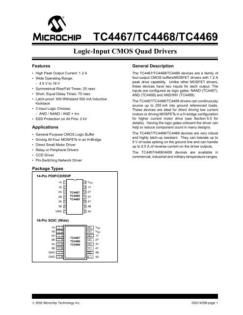
TC4467/TC4468/TC4469 - Microchip
TC4467/TC4468/TC4469 - Microchip
TC4467/TC4468/TC4469 - Microchip

You also want an ePaper? Increase the reach of your titles
YUMPU automatically turns print PDFs into web optimized ePapers that Google loves.
M <strong>TC4467</strong>/<strong>TC4468</strong>/<strong>TC4469</strong><br />
Features<br />
• High Peak Output Current: 1.2 A<br />
• Wide Operating Range:<br />
- 4.5 V to 18 V<br />
• Symmetrical Rise/Fall Times: 25 nsec<br />
• Short, Equal Delay Times: 75 nsec<br />
• Latch-proof. Will Withstand 500 mA Inductive<br />
Kickback<br />
• 3 Input Logic Choices:<br />
- AND / NAND / AND + Inv<br />
• ESD Protection on All Pins: 2 kV<br />
Applications<br />
• General Purpose CMOS Logic Buffer<br />
• Driving All Four MOSFETs in an H-Bridge<br />
• Direct Small Motor Driver<br />
• Relay or Peripheral Drivers<br />
• CCD Driver<br />
• Pin-Switching Network Driver<br />
Package Types<br />
14-Pin PDIP/CERDIP<br />
16-Pin SOIC (Wide)<br />
1A<br />
1B<br />
2A<br />
2B<br />
3A<br />
3B<br />
GND<br />
GND<br />
1A 1<br />
1B 2<br />
2A 3<br />
2B 4<br />
3A 5<br />
3B 6<br />
GND 7<br />
1<br />
2<br />
3<br />
4<br />
5<br />
6<br />
7<br />
8<br />
Logic-Input CMOS Quad Drivers<br />
<strong>TC4467</strong><br />
<strong>TC4468</strong><br />
<strong>TC4469</strong><br />
<strong>TC4467</strong><br />
<strong>TC4468</strong><br />
<strong>TC4469</strong><br />
14 VDD 13 1Y<br />
12 2Y<br />
11 3Y<br />
10 4Y<br />
9 4B<br />
8 4A<br />
16<br />
15<br />
14<br />
13<br />
12<br />
11<br />
10<br />
9<br />
VDD VDD 1Y<br />
2Y<br />
3Y<br />
4Y<br />
4B<br />
4A<br />
General Description<br />
The <strong>TC4467</strong>/<strong>TC4468</strong>/<strong>TC4469</strong> devices are a family of<br />
four-output CMOS buffers/MOSFET drivers with 1.2 A<br />
peak drive capability. Unlike other MOSFET drivers,<br />
these devices have two inputs for each output. The<br />
inputs are configured as logic gates: NAND (<strong>TC4467</strong>),<br />
AND (<strong>TC4468</strong>) and AND/INV (<strong>TC4469</strong>).<br />
The <strong>TC4467</strong>/<strong>TC4468</strong>/<strong>TC4469</strong> drivers can continuously<br />
source up to 250 mA into ground referenced loads.<br />
These devices are ideal for direct driving low current<br />
motors or driving MOSFETs in a H-bridge configuration<br />
for higher current motor drive (see Section 5.0 for<br />
details). Having the logic gates onboard the driver can<br />
help to reduce component count in many designs.<br />
The <strong>TC4467</strong>/<strong>TC4468</strong>/<strong>TC4469</strong> devices are very robust<br />
and highly latch-up resistant. They can tolerate up to<br />
5 V of noise spiking on the ground line and can handle<br />
up to 0.5 A of reverse current on the driver outputs.<br />
The <strong>TC4467</strong>/4468/4469 devices are available in<br />
commercial, industrial and military temperature ranges.<br />
© 2002 <strong>Microchip</strong> Technology Inc. DS21425B-page 1
<strong>TC4467</strong>/<strong>TC4468</strong>/<strong>TC4469</strong><br />
Logic Diagrams<br />
1A<br />
1B<br />
2A<br />
2B<br />
3A<br />
3B<br />
4A<br />
4B<br />
1<br />
2<br />
3<br />
4<br />
5<br />
6<br />
8<br />
9<br />
<strong>TC4467</strong><br />
V DD<br />
14<br />
7<br />
GND<br />
13<br />
12<br />
11<br />
10<br />
1Y<br />
2Y<br />
3Y<br />
4Y<br />
1A<br />
1B<br />
2A<br />
2B<br />
3A<br />
3B<br />
4A<br />
4B<br />
1<br />
2<br />
3<br />
4<br />
5<br />
6<br />
8<br />
9<br />
<strong>TC4468</strong><br />
VDD 14<br />
7<br />
GND<br />
13<br />
12<br />
11<br />
10<br />
<strong>TC4469</strong><br />
VDD 14<br />
7<br />
GND<br />
TC446X<br />
Output<br />
DS21425B-page 2 © 2002 <strong>Microchip</strong> Technology Inc.<br />
1Y<br />
2Y<br />
3Y<br />
4Y<br />
1A<br />
1B<br />
2A<br />
2B<br />
3A<br />
3B<br />
4A<br />
4B<br />
1<br />
2<br />
3<br />
4<br />
5<br />
6<br />
8<br />
9<br />
13<br />
12<br />
11<br />
10<br />
1Y<br />
2Y<br />
3Y<br />
4Y<br />
V DD
1.0 ELECTRICAL<br />
CHARACTERISTICS<br />
Absolute Maximum Ratings†<br />
Supply Voltage ...............................................................+20 V<br />
Input Voltage .............................(GND – 5 V) to (V DD + 0.3 V)<br />
Package Power Dissipation: (T A ≤ 70°C)<br />
PDIP...................................................................800 mW<br />
CERDIP .............................................................840 mW<br />
SOIC ..................................................................760 mW<br />
Package Thermal Resistance:<br />
CERDIP R θJ-A...................................................100°C/W<br />
CERDIP R θJ-C .....................................................23°C/W<br />
PDIP R θJ-A ..........................................................80°C/W<br />
PDIP R θJ-C..........................................................35°C/W<br />
SOIC R θJ-A ..........................................................95°C/W<br />
SOIC R θJ-C..........................................................28°C/W<br />
Operating Temperature Range:<br />
C Version ...................................................0°C to +70°C<br />
E Version.................................................-40°C to +85°C<br />
M Version ..............................................-55°C to +125°C<br />
Maximum Chip Temperature....................................... +150°C<br />
Storage Temperature Range.........................-65°C to +150°C<br />
ELECTRICAL SPECIFICATIONS<br />
Electrical Characteristics: Unless otherwise noted, T A = +25°C, with 4.5 V ≤ V DD ≤ 18 V.<br />
<strong>TC4467</strong>/<strong>TC4468</strong>/<strong>TC4469</strong><br />
†Notice: Stresses above those listed under "Maximum<br />
Ratings" may cause permanent damage to the device. This is<br />
a stress rating only and functional operation of the device at<br />
those or any other conditions above those indicated in the<br />
operation listings of this specification is not implied. Exposure<br />
to maximum rating conditions for extended periods may affect<br />
device reliability.<br />
Parameters Sym Min Typ Max Units Conditions<br />
Input<br />
Logic 1, High Input Voltage VIH 2.4 — VDD V Note 3<br />
Logic 0, Low Input Voltage VIL — — 0.8 V Note 3<br />
Input Current<br />
Output<br />
IIN -1.0 — +1.0 µA 0 V ≤ VIN ≤ VDD High Output Voltage VOH VDD – 0.025 — — V ILOAD = 100 µA (Note 1)<br />
Low Output Voltage VOL — — 0.15 V ILOAD = 10 mA (Note 1)<br />
Output Resistance RO — 10 15 Ω IOUT = 10 mA, VDD = 18 V<br />
Peak Output Current IPK — 1.2 — A<br />
Continuous Output Current IDC — — 300 mA Single Output<br />
— — 500 Total Package<br />
Latch-Up Protection Withstand<br />
Reverse Current<br />
Switching Time (Note 1)<br />
I — 500 — mA 4.5 V ≤ VDD ≤ 16 V<br />
Rise Time tR — 15 25 nsec Figure 4-1<br />
Fall Time tF — 15 25 nsec Figure 4-1<br />
Delay Time tD1 — 40 75 nsec Figure 4-1<br />
Delay Time<br />
Power Supply<br />
tD2 — 40 75 nsec Figure 4-1<br />
Power Supply Current IS — 1.5 4 mA<br />
Power Supply Voltage VDD 4.5 — 18 V Note 2<br />
Note 1: Totem pole outputs should not be paralleled because the propagation delay differences from one to the other could cause one driver to<br />
drive high a few nanoseconds before another. The resulting current spike, although short, may decrease the life of the device. Switching<br />
times are ensured by design.<br />
2: When driving all four outputs simultaneously in the same direction, VDD will be limited to 16 V. This reduces the chance that internal dv/dt<br />
will cause high-power dissipation in the device.<br />
3: The input threshold has approximately 50 mV of hysteresis centered at approximately 1.5 V. Input rise times should be kept below 5µsec<br />
to avoid high internal peak currents during input transitions. Static input levels should also be maintained above the maximum, or below<br />
the minimum, input levels specified in the "Electrical Characteristics" to avoid increased power dissipation in the device.<br />
© 2002 <strong>Microchip</strong> Technology Inc. DS21425B-page 3
<strong>TC4467</strong>/<strong>TC4468</strong>/<strong>TC4469</strong><br />
ELECTRICAL SPECIFICATIONS (OPERATING TEMPERATURES)<br />
Electrical Characteristics: Unless otherwise noted, over operating temperature range with 4.5 V ≤ V DD ≤ 18 V.<br />
TRUTH TABLE<br />
Parameters Sym Min Typ Max Units Conditions<br />
Input<br />
Logic 1, High Input Voltage VIH 2.4 — — V Note 3<br />
Logic 0, Low Input Voltage VIL — — 0.8 V Note 3<br />
Input Current<br />
Output<br />
IIN -10 — 10 µA 0 V ≤ VIN ≤ VDD High Output Voltage VOH VDD – 0.025 — — V ILOAD = 100 µA (Note 1)<br />
Low Output Voltage VOL — — 0.30 V ILOAD = 10 mA (Note 1)<br />
Output Resistance RO — 20 30 Ω IOUT = 10 mA, VDD = 18 V<br />
Peak Output Current IPK — 1.2 — A<br />
Continuous Output Current IDC — — 300 mA Single Output<br />
— — 500 Total Package<br />
Latch-Up Protection Withstand<br />
Reverse Current<br />
Switching Time (Note 1)<br />
I — 500 — mA 4.5 V ≤ VDD ≤ 16 V<br />
Rise Time tR — 15 50 nsec Figure 4-1<br />
Fall Time tF — 15 50 nsec Figure 4-1<br />
Delay Time tD1 — 40 100 nsec Figure 4-1<br />
Delay Time<br />
Power Supply<br />
tD2 — 40 100 nsec Figure 4-1<br />
Power Supply Current IS — — 8 mA<br />
Power Supply Voltage VDD 4.5 — 18 V Note 2<br />
Note 1: Totem pole outputs should not be paralleled because the propagation delay differences from one to the other could cause one driver to<br />
drive high a few nanoseconds before another. The resulting current spike, although short, may decrease the life of the device. Switching<br />
times are ensured by design.<br />
2: When driving all four outputs simultaneously in the same direction, VDD will be limited to 16 V. This reduces the chance that internal dv/dt<br />
will cause high-power dissipation in the device.<br />
3: The input threshold has approximately 50 mV of hysteresis centered at approximately 1.5 V. Input rise times should be kept below 5 µsec<br />
to avoid high internal peak currents during input transitions. Static input levels should also be maintained above the maximum, or below<br />
the minimum, input levels specified in the "Electrical Characteristics" to avoid increased power dissipation in the device.<br />
Part No. <strong>TC4467</strong> NAND <strong>TC4468</strong> AND <strong>TC4469</strong> AND/INV<br />
Inputs A H H L L H H L L H H L L<br />
Inputs B H L H L H L H L H L H L<br />
Outputs TC446X L H H H H L L L L H L L<br />
Legend: H = High L = Low<br />
DS21425B-page 4 © 2002 <strong>Microchip</strong> Technology Inc.
2.0 TYPICAL PERFORMANCE CURVES<br />
t RISE (nsec)<br />
Note: T A = +25°C, with 4.5 V ≤ V DD ≤ 18 V.<br />
FIGURE 2-1: Rise Time vs. Supply<br />
Voltage.<br />
t RISE (nsec)<br />
FIGURE 2-2: Rise Time vs. Capacitive<br />
Load.<br />
TIME (nsec)<br />
FIGURE 2-3: Rise/Fall Times vs.<br />
Temperature.<br />
<strong>TC4467</strong>/<strong>TC4468</strong>/<strong>TC4469</strong><br />
Note: The graphs and tables provided following this note are a statistical summary based on a limited number of<br />
samples and are provided for informational purposes only. The performance characteristics listed herein are<br />
not tested or guaranteed. In some graphs or tables, the data presented may be outside the specified<br />
operating range (e.g., outside specified power supply range) and therefore outside the warranted range.<br />
140<br />
120<br />
100<br />
80<br />
60<br />
40<br />
20<br />
140<br />
120<br />
100<br />
2200 0 ppF<br />
1600 ppF<br />
1000 pF<br />
470 pF<br />
100 pF<br />
0<br />
3 5 7 9 11 13 15 17 19<br />
VSUPPLY (V)<br />
80<br />
60<br />
40<br />
20<br />
25<br />
20<br />
15<br />
10<br />
5 V<br />
10 V<br />
15 V<br />
0<br />
100 1000<br />
CLOAD (pF)<br />
10,000<br />
5<br />
0 -50<br />
V SUPPLY = 17.5 V<br />
C LOAD = 470 pF<br />
t FALL<br />
t RISE<br />
-25 0 25 50 75 100 125<br />
TEMPERATURE (°C)<br />
FIGURE 2-4: Fall Time vs. Supply<br />
Voltage.<br />
FIGURE 2-5: Fall Time vs. Capacitive<br />
Load.<br />
FIGURE 2-6: Propagation Delay Time vs.<br />
Supply Voltage.<br />
© 2002 <strong>Microchip</strong> Technology Inc. DS21425B-page 5<br />
t FALL (nsec)<br />
t FALL (nsec)<br />
DELAY TIME (nsec)<br />
140<br />
120<br />
100<br />
80<br />
60<br />
40<br />
20<br />
140<br />
120<br />
100<br />
2200 pF<br />
1500 pF<br />
1000 pF<br />
470 pF<br />
100 ppF<br />
0<br />
3 5 7 9 11<br />
VSUPPLY (V)<br />
13 15 17 19<br />
80<br />
60<br />
40<br />
20<br />
0<br />
100<br />
80<br />
60<br />
40<br />
20<br />
0 4<br />
5 V<br />
10 V<br />
15 V<br />
1000 10,000<br />
CLOAD (pF)<br />
CLOAD = 470 4<br />
pF<br />
t D2<br />
t D1<br />
6 8 10 12 14 16 18<br />
VSUPPLY (V)
<strong>TC4467</strong>/<strong>TC4468</strong>/<strong>TC4469</strong><br />
2.0 TYPICAL PERFORMANCE CURVES (CONTINUED)<br />
DELAY TIME (nsec)<br />
Note: T A = +25°C, with 4.5 V ≤ V DD ≤ 18 V.<br />
140<br />
120<br />
100<br />
80<br />
60<br />
40<br />
20<br />
INPUT RISING<br />
INPUT FALLING<br />
0<br />
1 2 3 4 5 6 7 8 9 10<br />
VDRIVE (V)<br />
FIGURE 2-7: Input Amplitude vs. Delay<br />
Times.<br />
I QUIESCENT (mA)<br />
FIGURE 2-8: Quiescent Supply Current<br />
vs. Supply Voltage.<br />
R DS(ON) (Ω)<br />
2.5<br />
2.0<br />
1.5<br />
1.0<br />
0.5<br />
0 4<br />
35<br />
30<br />
25<br />
20<br />
15<br />
10<br />
5<br />
t D2<br />
t D1<br />
OUTPUTS = 0<br />
FIGURE 2-9: High-State Output<br />
Resistance.<br />
VDD = 12 V<br />
OUTPUTS = 1<br />
6 8 10 12 14 16 18<br />
VSUPPLY (V)<br />
T J = +150°C<br />
T J = +25°C<br />
0 4 6 8 10 12 14 16 18<br />
V SUPPLY (V)<br />
FIGURE 2-10: Propagation Delay Times<br />
vs. Temperatures.<br />
FIGURE 2-11: Quiescent Supply Current<br />
vs. Temperature.<br />
FIGURE 2-12: Low-State Output<br />
Resistance.<br />
DS21425B-page 6 © 2002 <strong>Microchip</strong> Technology Inc.<br />
DELAY TIME (nsec)<br />
I QUIESCENT (mA)<br />
R DS(ON) (Ω)<br />
70<br />
60<br />
50<br />
40<br />
30<br />
20<br />
-60<br />
3.5<br />
3.0<br />
2.5<br />
2.0<br />
1.5<br />
1.0<br />
0.5<br />
0<br />
-60<br />
35<br />
30<br />
25<br />
20<br />
15<br />
10<br />
5<br />
V DD = 17.5 V<br />
= 470 pF<br />
V IN<br />
t D1<br />
t D2<br />
-40 -20 0 20 40 60<br />
°C)<br />
80<br />
V DD = 17.5 V<br />
OUTPUTS = 1<br />
OUTPUTS = 0<br />
-40 -20 0 20 40 60 80<br />
TJUNCTION (°C)<br />
T J = +25°C<br />
100 120<br />
100 120<br />
0 4 6 8 10 12 14 16 18<br />
V SUPPLY (V)<br />
T J = +150°C
2.0 TYPICAL PERFORMANCE CURVES (CONTINUED)<br />
I SUPPLY (mA)<br />
Note: (Load on single output only).<br />
60<br />
50<br />
40<br />
30<br />
20<br />
10<br />
V DD = 18 V<br />
2MHz<br />
1 11MH MHz<br />
500 kHz<br />
200 kHz<br />
20 kHz<br />
0<br />
100 1000 10,000<br />
C LOAD (pF)<br />
FIGURE 2-13: Supply Current vs.<br />
Capacitive Load.<br />
I SUPPLY (mA)<br />
60<br />
50<br />
40<br />
30<br />
20<br />
10<br />
VDD = 12 V<br />
2MHz<br />
1 MHz<br />
500 kHz<br />
200 kHz<br />
20 kHz<br />
0<br />
100 1000 10,000<br />
C LOAD (pF)<br />
FIGURE 2-14: Supply Current vs.<br />
Capacitive Load.<br />
I SUPPLY (mA)<br />
60<br />
50<br />
40<br />
30<br />
VDD = 6 V<br />
2 MHz<br />
20<br />
10<br />
1 MHz<br />
500 kHz<br />
200 kHz<br />
0<br />
100 1000<br />
20 kHz<br />
10,000<br />
C LOAD (pF)<br />
FIGURE 2-15: Supply Current vs.<br />
Capacitive Load.<br />
<strong>TC4467</strong>/<strong>TC4468</strong>/<strong>TC4469</strong><br />
FIGURE 2-16: Supply Current vs.<br />
Frequency.<br />
FIGURE 2-17: Supply Current vs.<br />
Frequency.<br />
FIGURE 2-18: Supply Current vs.<br />
Frequency.<br />
© 2002 <strong>Microchip</strong> Technology Inc. DS21425B-page 7<br />
I SUPPLY (mA)<br />
I SUPPLY (mA)<br />
I SUPPLY (mA)<br />
60<br />
50<br />
40<br />
30<br />
20<br />
10<br />
V DD = 18 V<br />
2200 pF<br />
1000 pF<br />
100 ppF<br />
0<br />
10 100<br />
FREQUENCY (kHz)<br />
1000 10,000<br />
60<br />
50<br />
40<br />
30<br />
20<br />
10<br />
0 10 100<br />
FREQUENCY (kHz)<br />
60<br />
50<br />
40<br />
30<br />
20<br />
10<br />
VDD = 12 V<br />
V DD = 6 V<br />
1000<br />
0<br />
10 100<br />
FREQUENCY (kHz)<br />
1000<br />
2200 pF<br />
1000 ppF<br />
100 pF<br />
2200 pF<br />
1000 pF<br />
100 pF<br />
10,000<br />
10,000
<strong>TC4467</strong>/<strong>TC4468</strong>/<strong>TC4469</strong><br />
3.0 PIN DESCRIPTIONS<br />
The descriptions of the pins are listed in Table 3-1.<br />
TABLE 3-1: PIN FUNCTION TABLE<br />
14-Pin PDIP,<br />
CERDIP<br />
16-Pin SOIC<br />
(Wide)<br />
Symbol Symbol<br />
Description<br />
1A 1A Input A for Driver 1, TTL/CMOS Compatible Input<br />
1B 1B Input B for Driver 1, TTL/CMOS Compatible Input<br />
2A 2A Input A for Driver 2, TTL/CMOS Compatible Input<br />
2B 2B Input B for Driver 2, TTL/CMOS Compatible Input<br />
3A 3A Input A for Driver 3, TTL/CMOS Compatible Input<br />
3B 3B Input B for Driver 3, TTL/CMOS Compatible Input<br />
GND GND Ground<br />
— GND Ground<br />
4A 4A Input A for Driver 4, TTL/CMOS Compatible Input<br />
4B 4B Input B for Driver 4, TTL/CMOS Compatible Input<br />
4Y 4Y Output for Driver 4, CMOS Push-Pull Output<br />
3Y 3Y Output for Driver 3, CMOS Push-Pull Output<br />
2Y 2Y Output for Driver 2, CMOS Push-Pull Output<br />
1Y 1Y Output for Driver 1, CMOS Push-Pull Output<br />
VDD VDD Supply Input, 4.5 V to 18 V<br />
— VDD Supply Input, 4.5 V to 18 V<br />
DS21425B-page 8 © 2002 <strong>Microchip</strong> Technology Inc.
4.0 DETAILED DESCRIPTION<br />
4.1 Supply Bypassing<br />
Large currents are required to charge and discharge<br />
large capacitive loads quickly. For example, charging a<br />
1000 pF load to 18 V in 25 nsec requires 0.72 A from<br />
the device's power supply.<br />
To ensure low supply impedance over a wide frequency<br />
range, a 1 µF film capacitor in parallel with one or two<br />
low-inductance, 0.1 µF ceramic disk capacitors with<br />
short lead lengths (
<strong>TC4467</strong>/<strong>TC4468</strong>/<strong>TC4469</strong><br />
A resistive-load-caused dissipation for supplyreferenced<br />
loads is a function of duty cycle, load<br />
current and output voltage. The power dissipation is<br />
EQUATION<br />
Quiescent power dissipation depends on input signal<br />
duty cycle. Logic HIGH outputs result in a lower power<br />
dissipation mode, with only 0.6 mA total current drain<br />
(all devices driven). Logic LOW outputs raise the<br />
current to 4 mA maximum. The quiescent power<br />
dissipation is:<br />
EQUATION<br />
P L<br />
= DVOIL D = Duty Cycle<br />
VO = Device Output Voltage<br />
IL = Load Current<br />
P Q<br />
= VS( DI ( H)<br />
+ ( 1 – D)IL)<br />
IH = Quiescent Current with all outputs LOW<br />
(4 mA max.)<br />
IL = Quiescent Current with all outputs HIGH<br />
(0.6 mA max.)<br />
D = Duty Cycle<br />
VS = Supply Voltage<br />
Transition power dissipation arises in the complimentary<br />
configuration (TC446X) because the output stage<br />
N-channel and P-channel MOS transistors are ON<br />
simultaneously for a very short period when the output<br />
changes. The transition power dissipation is<br />
approximately:<br />
1 µF Film 0.1 µF Ceramic<br />
1A<br />
1B<br />
2A<br />
2B<br />
3A<br />
3B<br />
4A<br />
4B<br />
1<br />
2<br />
3<br />
4<br />
5<br />
6<br />
8<br />
9<br />
V DD<br />
7<br />
14<br />
V OUT<br />
470 pF<br />
FIGURE 4-1: Switching Time Test Circuit.<br />
13<br />
12<br />
11<br />
10<br />
+5 V<br />
Input<br />
(A, B)<br />
0V<br />
V DD<br />
Output<br />
0V<br />
EQUATION<br />
Package power dissipation is the sum of load,<br />
quiescent and transition power dissipations. An<br />
example shows the relative magnitude for each term:<br />
Maximum operating temperature is:<br />
EQUATION<br />
PT fVs 10 10 9 –<br />
= ( × )<br />
C = 1000 pF Capacitive Load<br />
VS = 15 V<br />
D = 50%<br />
f = 200 kHz<br />
Note: Ambient operating temperature should not<br />
exceed +85°C for "EJD" device or +125°C<br />
for "MJD" device.<br />
DS21425B-page 10 © 2002 <strong>Microchip</strong> Technology Inc.<br />
10%<br />
P D<br />
= Package Power Dissipation<br />
= PL + PQ + PT = 45mW + 35mW + 30mW<br />
= 110mW<br />
TJ – θJA( PD) = 141°C<br />
TJ = Maximum allowable junction temperature<br />
(+150°C )<br />
θJA = Junction-to-ambient thernal resistance<br />
(83.3°C/W) 14-pin plastic package<br />
Input: 100 kHz,<br />
square wave,<br />
t RISE = t FALL ≤ 10 nsec<br />
90%<br />
tD1 t R<br />
90%<br />
t D2<br />
10% 10%<br />
90%<br />
t F
5.0 APPLICATIONS INFORMATION<br />
FIGURE 5-1: Stepper Motor Drive.<br />
A<br />
B<br />
Direction<br />
Rev<br />
Fwd<br />
PWM Speed<br />
18 V<br />
+12 V<br />
FIGURE 5-2: Quad Driver For H-bridge Motor Control.<br />
1<br />
2<br />
3<br />
4<br />
5<br />
6<br />
8<br />
9<br />
1<br />
2<br />
3<br />
4<br />
5<br />
6<br />
8<br />
9<br />
<strong>TC4467</strong>/<strong>TC4468</strong>/<strong>TC4469</strong><br />
14<br />
<strong>TC4469</strong><br />
7<br />
+5 V to +15 V<br />
14<br />
<strong>TC4469</strong><br />
7<br />
© 2002 <strong>Microchip</strong> Technology Inc. DS21425B-page 11<br />
13<br />
12<br />
11<br />
10<br />
13<br />
12<br />
11<br />
10<br />
Red<br />
Gray<br />
Yel<br />
Blk<br />
Airpax<br />
#M82102-P2<br />
7.5/Step<br />
Motor<br />
M<br />
Motor
<strong>TC4467</strong>/<strong>TC4468</strong>/<strong>TC4469</strong><br />
6.0 PACKAGING INFORMATION<br />
6.1 Package Marking Information<br />
14-Lead PDIP (300 mil) Example:<br />
XXXXXXXXXXXXXX<br />
XXXXXXXXXXXXXX<br />
YYWWNNN<br />
14-Lead CERDIP (300 mil) Example:<br />
XXXXXXXXXXXXXX<br />
XXXXXXXXXXXXXX<br />
YYWWNNN<br />
16-Lead SOIC (300 mil) Example:<br />
XXXXXXXXXXX<br />
XXXXXXXXXXX<br />
XXXXXXXXXXX<br />
YYWWNNN<br />
Legend: XX...X Customer specific information*<br />
YY Year code (last 2 digits of calendar year)<br />
WW Week code (week of January 1 is week ‘01’)<br />
NNN Alphanumeric traceability code<br />
<strong>TC4469</strong>COE<br />
YYWWNNN<br />
<strong>TC4467</strong>CPD<br />
YYWWNNN<br />
<strong>TC4468</strong>EJD<br />
YYWWNNN<br />
Note: In the event the full <strong>Microchip</strong> part number cannot be marked on one line, it will<br />
be carried over to the next line thus limiting the number of available characters<br />
for customer specific information.<br />
* Standard OTP marking consists of <strong>Microchip</strong> part number, year code, week code, facility code, mask<br />
rev#, and assembly code.<br />
DS21425B-page 12 © 2002 <strong>Microchip</strong> Technology Inc.
14-Lead Plastic Dual In-line (P) – 300 mil (PDIP)<br />
n<br />
β<br />
E1<br />
E<br />
eB<br />
2<br />
1<br />
c<br />
D<br />
A<br />
A1<br />
<strong>TC4467</strong>/<strong>TC4468</strong>/<strong>TC4469</strong><br />
Units INCHES* MILLIMETERS<br />
Dimension Limits MIN NOM MAX MIN NOM MAX<br />
Number of Pins n 14 14<br />
Pitch p .100 2.54<br />
Top to Seating Plane A .140 .155 .170 3.56 3.94 4.32<br />
Molded Package Thickness A2 .115 .130 .145 2.92 3.30 3.68<br />
Base to Seating Plane A1 .015 0.38<br />
Shoulder to Shoulder Width E .300 .313 .325 7.62 7.94 8.26<br />
Molded Package Width E1 .240 .250 .260 6.10 6.35 6.60<br />
Overall Length D .740 .750 .760 18.80 19.05 19.30<br />
Tip to Seating Plane L .125 .130 .135 3.18 3.30 3.43<br />
Lead Thickness c .008 .012 .015 0.20 0.29 0.38<br />
Upper Lead Width B1 .045 .058 .070 1.14 1.46 1.78<br />
Lower Lead Width B .014 .018 .022 0.36 0.46 0.56<br />
Overall Row Spacing § eB .310 .370 .430 7.87 9.40 10.92<br />
Mold Draft Angle Top α 5 10 15 5 10 15<br />
Mold Draft Angle Bottom<br />
* Controlling Parameter<br />
§ Significant Characteristic<br />
Notes:<br />
β 5 10 15 5 10 15<br />
Dimensions D and E1 do not include mold flash or protrusions. Mold flash or protrusions shall not exceed<br />
.010” (0.254mm) per side.<br />
JEDEC Equivalent: MS-001<br />
Drawing No. C04-005<br />
© 2002 <strong>Microchip</strong> Technology Inc. DS21425B-page 13<br />
B<br />
B1<br />
p<br />
α<br />
A2<br />
L
<strong>TC4467</strong>/<strong>TC4468</strong>/<strong>TC4469</strong><br />
14-Lead Ceramic Dual In-line – 300 mil (CERDIP)<br />
14-Pin CERDIP (Narrow)<br />
.200 (5.08)<br />
.160 (4.06)<br />
.200 (5.08)<br />
.125 (3.18)<br />
.098 (2.49) MAX.<br />
.110 (2.79)<br />
.090 (2.29)<br />
.780 (19.81)<br />
.740 (18.80)<br />
.065 (1.65)<br />
.045 (1.14)<br />
.030 (0.76) MIN.<br />
.020 (0.51)<br />
.016 (0.41)<br />
.300 (7.62)<br />
.230 (5.84)<br />
.040 (1.02)<br />
.020 (0.51)<br />
.015 (0.38)<br />
.008 (0.20)<br />
.400 (10.16)<br />
.320 (8.13)<br />
DS21425B-page 14 © 2002 <strong>Microchip</strong> Technology Inc.<br />
PIN 1<br />
.150 (3.81)<br />
MIN.<br />
.320 (8.13)<br />
.290 (7.37)<br />
3° MIN.<br />
Dimensions: inches (mm)
16-Lead Plastic Small Outline (SO) – Wide, 300 mil (SOIC)<br />
B<br />
c<br />
p<br />
n<br />
45°<br />
β<br />
E<br />
E1<br />
h<br />
2<br />
1<br />
L<br />
D<br />
φ<br />
<strong>TC4467</strong>/<strong>TC4468</strong>/<strong>TC4469</strong><br />
Units<br />
INCHES*<br />
MILLIMETERS<br />
Dimension Limits MIN NOM MAX MIN NOM MAX<br />
Number of Pins<br />
n<br />
16<br />
16<br />
Pitch<br />
p<br />
.050<br />
1.27<br />
Overall Height<br />
A .093 .099 .104 2.36 2.50 2.64<br />
Molded Package Thickness A2 .088 .091 .094 2.24 2.31 2.39<br />
Standoff §<br />
A1 .004 .008 .012 0.10 0.20 0.30<br />
Overall Width<br />
E .394 .407 .420 10.01 10.34 10.67<br />
Molded Package Width<br />
E1 .291 .295 .299 7.39 7.49 7.59<br />
Overall Length<br />
D .398 .406 .413 10.10 10.30 10.49<br />
Chamfer Distance<br />
h .010 .020 .029 0.25 0.50 0.74<br />
Foot Length<br />
L .016 .033 .050 0.41 0.84 1.27<br />
Foot Angle φ 0 4 8 0 4 8<br />
Lead Thickness<br />
c .009 .011 .013 0.23 0.28 0.33<br />
Lead Width<br />
B .014 .017 .020 0.36 0.42 0.51<br />
Mold Draft Angle Top<br />
α<br />
0 12 15<br />
0 12 15<br />
Mold Draft Angle Bottom<br />
β<br />
0 12 15<br />
0 12 15<br />
* Controlling Parameter<br />
§ Significant Characteristic<br />
Notes:<br />
Dimensions D and E1 do not include mold flash or protrusions. Mold flash or protrusions shall not exceed<br />
.010” (0.254mm) per side.<br />
JEDEC Equivalent: MS-013<br />
Drawing No. C04-102<br />
© 2002 <strong>Microchip</strong> Technology Inc. DS21425B-page 15<br />
A<br />
A1<br />
α<br />
A2
<strong>TC4467</strong>/<strong>TC4468</strong>/<strong>TC4469</strong><br />
NOTES:<br />
DS21425B-page 16 © 2002 <strong>Microchip</strong> Technology Inc.
ON-LINE SUPPORT<br />
<strong>Microchip</strong> provides on-line support on the <strong>Microchip</strong><br />
World Wide Web (WWW) site.<br />
The web site is used by <strong>Microchip</strong> as a means to make<br />
files and information easily available to customers. To<br />
view the site, the user must have access to the Internet<br />
and a web browser, such as Netscape or Microsoft<br />
Explorer. Files are also available for FTP download<br />
from our FTP site.<br />
Connecting to the <strong>Microchip</strong> Internet Web Site<br />
The <strong>Microchip</strong> web site is available by using your<br />
favorite Internet browser to attach to:<br />
www.microchip.com<br />
The file transfer site is available by using an FTP service<br />
to connect to:<br />
ftp://ftp.microchip.com<br />
The web site and file transfer site provide a variety of<br />
services. Users may download files for the latest<br />
Development Tools, Data Sheets, Application Notes,<br />
User's Guides, Articles and Sample Programs. A variety<br />
of <strong>Microchip</strong> specific business information is also<br />
available, including listings of <strong>Microchip</strong> sales offices,<br />
distributors and factory representatives. Other data<br />
available for consideration is:<br />
• Latest <strong>Microchip</strong> Press Releases<br />
• Technical Support Section with Frequently Asked<br />
Questions<br />
• Design Tips<br />
• Device Errata<br />
• Job Postings<br />
• <strong>Microchip</strong> Consultant Program Member Listing<br />
• Links to other useful web sites related to<br />
<strong>Microchip</strong> Products<br />
• Conferences for products, Development Systems,<br />
technical information and more<br />
• Listing of seminars and events<br />
<strong>TC4467</strong>/<strong>TC4468</strong>/<strong>TC4469</strong><br />
Systems Information and Upgrade Hot Line<br />
The Systems Information and Upgrade Line provides<br />
system users a listing of the latest versions of all of<br />
<strong>Microchip</strong>'s development systems software products.<br />
Plus, this line provides information on how customers<br />
can receive any currently available upgrade kits.The<br />
Hot Line Numbers are:<br />
1-800-755-2345 for U.S. and most of Canada, and<br />
1-480-792-7302 for the rest of the world.<br />
013001<br />
© 2002 <strong>Microchip</strong> Technology Inc. DS21425B-page17
<strong>TC4467</strong>/<strong>TC4468</strong>/<strong>TC4469</strong><br />
READER RESPONSE<br />
It is our intention to provide you with the best documentation possible to ensure successful use of your <strong>Microchip</strong> product.<br />
If you wish to provide your comments on organization, clarity, subject matter, and ways in which our documentation<br />
can better serve you, please FAX your comments to the Technical Publications Manager at (480) 792-4150.<br />
Please list the following information, and use this outline to provide us with your comments about this Data Sheet.<br />
To: Technical Publications Manager<br />
RE: Reader Response<br />
From: Name<br />
Company<br />
Address<br />
City / State / ZIP / Country<br />
Telephone: (_______) _________ - _________<br />
Application (optional):<br />
Would you like a reply? Y N<br />
Device: <strong>TC4467</strong>/<strong>TC4468</strong>/<strong>TC4469</strong><br />
Questions:<br />
1. What are the best features of this document?<br />
2. How does this document meet your hardware and software development needs?<br />
3. Do you find the organization of this data sheet easy to follow? If not, why?<br />
4. What additions to the data sheet do you think would enhance the structure and subject?<br />
5. What deletions from the data sheet could be made without affecting the overall usefulness?<br />
6. Is there any incorrect or misleading information (what and where)?<br />
7. How would you improve this document?<br />
Literature Number:<br />
DS21425B<br />
8. How would you improve our software, systems, and silicon products?<br />
Total Pages Sent<br />
FAX: (______) _________ - _________<br />
DS21425B-page18 © 2002 <strong>Microchip</strong> Technology Inc.
PRODUCT IDENTIFICATION SYSTEM<br />
<strong>TC4467</strong>/<strong>TC4468</strong>/<strong>TC4469</strong><br />
To order or obtain information, e.g., on pricing or delivery, refer to the factory or the listed sales office.<br />
PART NO. X XX<br />
Device<br />
Sales and Support<br />
Temperature<br />
Range<br />
Package<br />
Device: <strong>TC4467</strong>: 1.2A Quad MOSFET Driver, NAND<br />
<strong>TC4468</strong>: 1.2A Quad MOSFET Driver, AND<br />
<strong>TC4469</strong>: 1.2A Quad MOSFET Driver, AND/INV<br />
Temperature Range: C = 0°C to +70°C<br />
E = -40°C to +85°C (CERDIP only)<br />
M = -55°C to +125°C (CERDIP only)<br />
Package: PD = Plastic DIP, (300 mil body), 14-lead<br />
JD = Ceramic DIP, (300 mil body), 14-lead<br />
OE = SOIC (Wide), 16-lead<br />
OE713 = SOIC (Wide), 16-lead (Tape and Reel)<br />
Data Sheets<br />
Products supported by a preliminary Data Sheet may have an errata sheet describing minor operational differences and recommended<br />
workarounds. To determine if an errata sheet exists for a particular device, please contact one of the following:<br />
1. Your local <strong>Microchip</strong> sales office<br />
2. The <strong>Microchip</strong> Corporate Literature Center U.S. FAX: (480) 792-7277<br />
3. The <strong>Microchip</strong> Worldwide Site (www.microchip.com)<br />
Examples:<br />
Please specify which device, revision of silicon and Data Sheet (include Literature #) you are using.<br />
a) <strong>TC4467</strong>COE: Commerical Temperature,<br />
SOIC package.<br />
b) <strong>TC4467</strong>CPD: Commercial Temperature,<br />
PDIP package.<br />
c) <strong>TC4467</strong>MJD: Military Temperature,<br />
Ceramic DIP package.<br />
a) <strong>TC4468</strong>COE713: Tape and Reel,<br />
Commerical Temp., SOIC package.<br />
b) <strong>TC4468</strong>CPD: Commercial Temperature,<br />
PDIP package.<br />
a) <strong>TC4469</strong>COE: Commercial Temperature,<br />
SOIC package.<br />
b) <strong>TC4469</strong>CPD: Commercial Temperature,<br />
PDIP package.<br />
New Customer Notification System<br />
Register on our web site (www.microchip.com/cn) to receive the most current information on our products.<br />
© 2002 <strong>Microchip</strong> Technology Inc. DS21425B-page19
<strong>TC4467</strong>/<strong>TC4468</strong>/<strong>TC4469</strong><br />
NOTES:<br />
DS21425B-page 20 © 2002 <strong>Microchip</strong> Technology Inc.
Information contained in this publication regarding device<br />
applications and the like is intended through suggestion only<br />
and may be superseded by updates. It is your responsibility to<br />
ensure that your application meets with your specifications.<br />
No representation or warranty is given and no liability is<br />
assumed by <strong>Microchip</strong> Technology Incorporated with respect<br />
to the accuracy or use of such information, or infringement of<br />
patents or other intellectual property rights arising from such<br />
use or otherwise. Use of <strong>Microchip</strong>’s products as critical components<br />
in life support systems is not authorized except with<br />
express written approval by <strong>Microchip</strong>. No licenses are conveyed,<br />
implicitly or otherwise, under any intellectual property<br />
rights.<br />
<strong>TC4467</strong>/<strong>TC4468</strong>/<strong>TC4469</strong><br />
Trademarks<br />
The <strong>Microchip</strong> name and logo, the <strong>Microchip</strong> logo, FilterLab,<br />
KEELOQ, microID, MPLAB, MXDEV, PIC, PICmicro,<br />
PICMASTER, PICSTART, PRO MATE, SEEVAL and The<br />
Embedded Control Solutions Company are registered trademarks<br />
of <strong>Microchip</strong> Technology Incorporated in the U.S.A. and<br />
other countries.<br />
dsPIC, dsPICDEM.net, ECONOMONITOR, FanSense,<br />
FlexROM, fuzzyLAB, In-Circuit Serial Programming, ICSP,<br />
ICEPIC, microPort, Migratable Memory, MPASM, MPLIB,<br />
MPLINK, MPSIM, MXLAB, PICC, PICDEM, PICDEM.net,<br />
rfPIC, Select Mode and Total Endurance are trademarks of<br />
<strong>Microchip</strong> Technology Incorporated in the U.S.A.<br />
Serialized Quick Turn Programming (SQTP) is a service mark<br />
of <strong>Microchip</strong> Technology Incorporated in the U.S.A.<br />
All other trademarks mentioned herein are property of their<br />
respective companies.<br />
© 2002, <strong>Microchip</strong> Technology Incorporated, Printed in the<br />
U.S.A., All Rights Reserved.<br />
Printed on recycled paper.<br />
<strong>Microchip</strong> received QS-9000 quality system<br />
certification for its worldwide headquarters,<br />
design and wafer fabrication facilities in<br />
Chandler and Tempe, Arizona in July 1999<br />
and Mountain View, California in March 2002.<br />
The Company’s quality system processes and<br />
procedures are QS-9000 compliant for its<br />
PICmicro ® 8-bit MCUs, KEELOQ ® code hopping<br />
devices, Serial EEPROMs, microperipherals,<br />
non-volatile memory and analog products. In<br />
addition, <strong>Microchip</strong>’s quality system for the<br />
design and manufacture of development<br />
systems is ISO 9001 certified.<br />
© 2002 <strong>Microchip</strong> Technology Inc. DS21425B-page 21
M<br />
AMERICAS<br />
Corporate Office<br />
2355 West Chandler Blvd.<br />
Chandler, AZ 85224-6199<br />
Tel: 480-792-7200 Fax: 480-792-7277<br />
Technical Support: 480-792-7627<br />
Web Address: http://www.microchip.com<br />
Rocky Mountain<br />
2355 West Chandler Blvd.<br />
Chandler, AZ 85224-6199<br />
Tel: 480-792-7966 Fax: 480-792-4338<br />
Atlanta<br />
500 Sugar Mill Road, Suite 200B<br />
Atlanta, GA 30350<br />
Tel: 770-640-0034 Fax: 770-640-0307<br />
Boston<br />
2 Lan Drive, Suite 120<br />
Westford, MA 01886<br />
Tel: 978-692-3848 Fax: 978-692-3821<br />
Chicago<br />
333 Pierce Road, Suite 180<br />
Itasca, IL 60143<br />
Tel: 630-285-0071 Fax: 630-285-0075<br />
Dallas<br />
4570 Westgrove Drive, Suite 160<br />
Addison, TX 75001<br />
Tel: 972-818-7423 Fax: 972-818-2924<br />
Detroit<br />
Tri-Atria Office Building<br />
32255 Northwestern Highway, Suite 190<br />
Farmington Hills, MI 48334<br />
Tel: 248-538-2250 Fax: 248-538-2260<br />
Kokomo<br />
2767 S. Albright Road<br />
Kokomo, Indiana 46902<br />
Tel: 765-864-8360 Fax: 765-864-8387<br />
Los Angeles<br />
18201 Von Karman, Suite 1090<br />
Irvine, CA 92612<br />
Tel: 949-263-1888 Fax: 949-263-1338<br />
New York<br />
150 Motor Parkway, Suite 202<br />
Hauppauge, NY 11788<br />
Tel: 631-273-5305 Fax: 631-273-5335<br />
San Jose<br />
<strong>Microchip</strong> Technology Inc.<br />
2107 North First Street, Suite 590<br />
San Jose, CA 95131<br />
Tel: 408-436-7950 Fax: 408-436-7955<br />
Toronto<br />
6285 Northam Drive, Suite 108<br />
Mississauga, Ontario L4V 1X5, Canada<br />
Tel: 905-673-0699 Fax: 905-673-6509<br />
WORLDWIDE SALES AND SERVICE<br />
ASIA/PACIFIC<br />
Australia<br />
<strong>Microchip</strong> Technology Australia Pty Ltd<br />
Suite 22, 41 Rawson Street<br />
Epping 2121, NSW<br />
Australia<br />
Tel: 61-2-9868-6733 Fax: 61-2-9868-6755<br />
China - Beijing<br />
<strong>Microchip</strong> Technology Consulting (Shanghai)<br />
Co., Ltd., Beijing Liaison Office<br />
Unit 915<br />
Bei Hai Wan Tai Bldg.<br />
No. 6 Chaoyangmen Beidajie<br />
Beijing, 100027, No. China<br />
Tel: 86-10-85282100 Fax: 86-10-85282104<br />
China - Chengdu<br />
<strong>Microchip</strong> Technology Consulting (Shanghai)<br />
Co., Ltd., Chengdu Liaison Office<br />
Rm. 2401, 24th Floor,<br />
Ming Xing Financial Tower<br />
No. 88 TIDU Street<br />
Chengdu 610016, China<br />
Tel: 86-28-86766200 Fax: 86-28-86766599<br />
China - Fuzhou<br />
<strong>Microchip</strong> Technology Consulting (Shanghai)<br />
Co., Ltd., Fuzhou Liaison Office<br />
Unit 28F, World Trade Plaza<br />
No. 71 Wusi Road<br />
Fuzhou 350001, China<br />
Tel: 86-591-7503506 Fax: 86-591-7503521<br />
China - Shanghai<br />
<strong>Microchip</strong> Technology Consulting (Shanghai)<br />
Co., Ltd.<br />
Room 701, Bldg. B<br />
Far East International Plaza<br />
No. 317 Xian Xia Road<br />
Shanghai, 200051<br />
Tel: 86-21-6275-5700 Fax: 86-21-6275-5060<br />
China - Shenzhen<br />
<strong>Microchip</strong> Technology Consulting (Shanghai)<br />
Co., Ltd., Shenzhen Liaison Office<br />
Rm. 1315, 13/F, Shenzhen Kerry Centre,<br />
Renminnan Lu<br />
Shenzhen 518001, China<br />
Tel: 86-755-2350361 Fax: 86-755-2366086<br />
China - Hong Kong SAR<br />
<strong>Microchip</strong> Technology Hongkong Ltd.<br />
Unit 901-6, Tower 2, Metroplaza<br />
223 Hing Fong Road<br />
Kwai Fong, N.T., Hong Kong<br />
Tel: 852-2401-1200 Fax: 852-2401-3431<br />
India<br />
<strong>Microchip</strong> Technology Inc.<br />
India Liaison Office<br />
Divyasree Chambers<br />
1 Floor, Wing A (A3/A4)<br />
No. 11, O’Shaugnessey Road<br />
Bangalore, 560 025, India<br />
Tel: 91-80-2290061 Fax: 91-80-2290062<br />
Japan<br />
<strong>Microchip</strong> Technology Japan K.K.<br />
Benex S-1 6F<br />
3-18-20, Shinyokohama<br />
Kohoku-Ku, Yokohama-shi<br />
Kanagawa, 222-0033, Japan<br />
Tel: 81-45-471- 6166 Fax: 81-45-471-6122<br />
Korea<br />
<strong>Microchip</strong> Technology Korea<br />
168-1, Youngbo Bldg. 3 Floor<br />
Samsung-Dong, Kangnam-Ku<br />
Seoul, Korea 135-882<br />
Tel: 82-2-554-7200 Fax: 82-2-558-5934<br />
Singapore<br />
<strong>Microchip</strong> Technology Singapore Pte Ltd.<br />
200 Middle Road<br />
#07-02 Prime Centre<br />
Singapore, 188980<br />
Tel: 65-6334-8870 Fax: 65-6334-8850<br />
Taiwan<br />
<strong>Microchip</strong> Technology (Barbados) Inc.,<br />
Taiwan Branch<br />
11F-3, No. 207<br />
Tung Hua North Road<br />
Taipei, 105, Taiwan<br />
Tel: 886-2-2717-7175 Fax: 886-2-2545-0139<br />
EUROPE<br />
Denmark<br />
<strong>Microchip</strong> Technology Nordic ApS<br />
Regus Business Centre<br />
Lautrup hoj 1-3<br />
Ballerup DK-2750 Denmark<br />
Tel: 45 4420 9895 Fax: 45 4420 9910<br />
France<br />
<strong>Microchip</strong> Technology SARL<br />
Parc d’Activite du Moulin de Massy<br />
43 Rue du Saule Trapu<br />
Batiment A - ler Etage<br />
91300 Massy, France<br />
Tel: 33-1-69-53-63-20 Fax: 33-1-69-30-90-79<br />
Germany<br />
<strong>Microchip</strong> Technology GmbH<br />
Gustav-Heinemann Ring 125<br />
D-81739 Munich, Germany<br />
Tel: 49-89-627-144 0 Fax: 49-89-627-144-44<br />
Italy<br />
<strong>Microchip</strong> Technology SRL<br />
Centro Direzionale Colleoni<br />
Palazzo Taurus 1 V. Le Colleoni 1<br />
20041 Agrate Brianza<br />
Milan, Italy<br />
Tel: 39-039-65791-1 Fax: 39-039-6899883<br />
United Kingdom<br />
<strong>Microchip</strong> Ltd.<br />
505 Eskdale Road<br />
Winnersh Triangle<br />
Wokingham<br />
Berkshire, England RG41 5TU<br />
Tel: 44 118 921 5869 Fax: 44-118 921-5820<br />
Austria<br />
<strong>Microchip</strong> Technology Austria GmbH<br />
Durisolstrasse 2<br />
A-4600 Wels<br />
Austria<br />
Tel: 43-7242-2244-399<br />
Fax: 43-7242-2244-393<br />
DS21425B-page 22 © 2002 <strong>Microchip</strong> Technology Inc.<br />
05/16/02