MCP23017 - Microchip
MCP23017 - Microchip
MCP23017 - Microchip

Create successful ePaper yourself
Turn your PDF publications into a flip-book with our unique Google optimized e-Paper software.
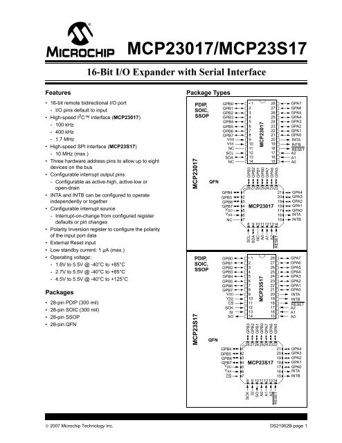
Features<br />
• 16-bit remote bidirectional I/O port<br />
- I/O pins default to input<br />
• High-speed I 2 C interface (<strong>MCP23017</strong>)<br />
- 100 kHz<br />
- 400 kHz<br />
- 1.7 MHz<br />
• High-speed SPI interface (MCP23S17)<br />
- 10 MHz (max.)<br />
• Three hardware address pins to allow up to eight<br />
devices on the bus<br />
• Configurable interrupt output pins<br />
- Configurable as active-high, active-low or<br />
open-drain<br />
• INTA and INTB can be configured to operate<br />
independently or together<br />
• Configurable interrupt source<br />
- Interrupt-on-change from configured register<br />
defaults or pin changes<br />
• Polarity Inversion register to configure the polarity<br />
of the input port data<br />
• External Reset input<br />
• Low standby current: 1 µA (max.)<br />
• Operating voltage:<br />
- 1.8V to 5.5V @ -40°C to +85°C<br />
- 2.7V to 5.5V @ -40°C to +85°C<br />
- 4.5V to 5.5V @ -40°C to +125°C<br />
Packages<br />
• 28-pin PDIP (300 mil)<br />
• 28-pin SOIC (300 mil)<br />
• 28-pin SSOP<br />
• 28-pin QFN<br />
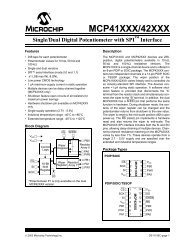
<strong>MCP23017</strong>/MCP23S17<br />
16-Bit I/O Expander with Serial Interface<br />
Package Types<br />
PDIP,<br />
SOIC,<br />
SSOP<br />
© 2007 <strong>Microchip</strong> Technology Inc. DS21952B-page 1<br />
MCP23S17 <strong>MCP23017</strong><br />
PDIP,<br />
SOIC,<br />
SSOP<br />
QFN<br />
GPB0<br />
GPB1<br />
GPB2<br />
GPB3<br />
GPB4<br />
GPB5<br />
GPB6<br />
GPB7<br />
VDD<br />
VSS<br />
NC<br />
SCL<br />
SDA<br />
NC<br />
• 1<br />
2<br />
3<br />
4<br />
5<br />
6<br />
7<br />
8<br />
9<br />
10<br />
11<br />
12<br />
13<br />
14<br />
<strong>MCP23017</strong><br />
28<br />
27<br />
26<br />
25<br />
24<br />
23<br />
22<br />
21<br />
20<br />
19<br />
18<br />
17<br />
16<br />
15<br />
GPB3<br />
GPB2<br />
GPB1<br />
GPB0<br />
GPA7<br />
GPA6<br />
GPA5<br />
28272625242322 GPB4 1<br />
21 GPA4<br />
GPB5 2<br />
20 GPA3<br />
GPB6 3<br />
19 GPA2<br />
GPB7<br />
VDD VSS 4<br />
5<br />
6<br />
<strong>MCP23017</strong> 18<br />
17<br />
16<br />
GPA1<br />
GPA0<br />
INTA<br />
NC 7<br />
15 INTB<br />
8 9 1011 121314<br />
GPB0<br />
GPB1<br />
GPB2<br />
GPB3<br />
GPB4<br />
GPB5<br />
GPB6<br />
GPB7<br />
VDD<br />
VSS<br />
CS<br />
SCK<br />
SI<br />
SO<br />
SCL<br />
SDA<br />
NC<br />
A0<br />
A1<br />
A2<br />
RESET<br />
• 1<br />
2<br />
3<br />
4<br />
5<br />
6<br />
7<br />
8<br />
9<br />
10<br />
11<br />
12<br />
13<br />
14<br />
MCP23S17<br />
28<br />
27<br />
26<br />
25<br />
24<br />
23<br />
22<br />
21<br />
20<br />
19<br />
18<br />
17<br />
16<br />
15<br />
GPB3<br />
GPB2<br />
GPB1<br />
GPB0<br />
GPA7<br />
GPA6<br />
GPA5<br />
GPA7<br />
GPA6<br />
GPA5<br />
GPA4<br />
GPA3<br />
GPA2<br />
GPA1<br />
GPA0<br />
INTA<br />
INTB<br />
RESET<br />
A2<br />
A1<br />
A0<br />
GPA7<br />
GPA6<br />
GPA5<br />
GPA4<br />
GPA3<br />
GPA2<br />
GPA1<br />
GPA0<br />
INTA<br />
INTB<br />
RESET<br />
A2<br />
A1<br />
A0<br />
QFN<br />
28272625242322 GPB4 1<br />
21 GPA4<br />
GPB5 2<br />
20 GPA3<br />
GPB6 3<br />
19 GPA2<br />
GPB7<br />
VDD VSS 4<br />
5<br />
6<br />
MCP23S17 18<br />
17<br />
16<br />
GPA1<br />
GPA0<br />
INTA<br />
CS 7<br />
15 INTB<br />
8 9 1011 121314<br />
SCK<br />
SI<br />
SO<br />
A0<br />
A1<br />
A2<br />
RESET
<strong>MCP23017</strong>/MCP23S17<br />
Functional Block Diagram<br />
CS<br />
SCK<br />
SI<br />
SO<br />
SCL<br />
SDA<br />
A2:A0<br />
RESET<br />
INTA<br />
INTB<br />
SPI<br />
I 2 C<br />
3<br />
Decode<br />
Interrupt<br />
Logic<br />
MCP23S17<br />
<strong>MCP23017</strong><br />
Serializer/<br />
Deserializer<br />
Control<br />
8<br />
Configuration/<br />
Control<br />
Registers<br />
GPB7<br />
GPB6<br />
GPB5<br />
GPB4<br />
GPB3<br />
GPB2<br />
GPB1<br />
GPB0<br />
DS21952B-page 2 © 2007 <strong>Microchip</strong> Technology Inc.<br />
16<br />
GPIO<br />
GPIO<br />
GPA7<br />
GPA6<br />
GPA5<br />
GPA4<br />
GPA3<br />
GPA2<br />
GPA1<br />
GPA0
1.0 DEVICE OVERVIEW<br />
The <strong>MCP23017</strong>/MCP23S17 (MCP23X17) device<br />
family provides 16-bit, general purpose parallel I/O<br />
expansion for I 2 C bus or SPI applications. The two<br />
devices differ only in the serial interface.<br />
• <strong>MCP23017</strong> – I 2 C interface<br />
• MCP23S17 – SPI interface<br />
The MCP23X17 consists of multiple 8-bit configuration<br />
registers for input, output and polarity selection. The<br />
system master can enable the I/Os as either inputs or<br />
outputs by writing the I/O configuration bits (IODIRA/B).<br />
The data for each input or output is kept in the<br />
corresponding input or output register. The polarity of<br />
the Input Port register can be inverted with the Polarity<br />
Inversion register. All registers can be read by the<br />
system master.<br />
The 16-bit I/O port functionally consists of two 8-bit<br />
ports (PORTA and PORTB). The MCP23X17 can be<br />
configured to operate in the 8-bit or 16-bit modes via<br />
IOCON.BANK.<br />
<strong>MCP23017</strong>/MCP23S17<br />
There are two interrupt pins, INTA and INTB, that can<br />
be associated with their respective ports, or can be<br />
logically OR’ed together so that both pins will activate if<br />
either port causes an interrupt.<br />
The interrupt output can be configured to activate<br />
under two conditions (mutually exclusive):<br />
1. When any input state differs from its<br />
corresponding Input Port register state. This is<br />
used to indicate to the system master that an<br />
input state has changed.<br />
2. When an input state differs from a preconfigured<br />
register value (DEFVAL register).<br />
The Interrupt Capture register captures port values at<br />
the time of the interrupt, thereby saving the condition<br />
that caused the interrupt.<br />
The Power-on Reset (POR) sets the registers to their<br />
default values and initializes the device state machine.<br />
The hardware address pins are used to determine the<br />
device address.<br />
© 2007 <strong>Microchip</strong> Technology Inc. DS21952B-page 3
<strong>MCP23017</strong>/MCP23S17<br />
1.1 Pin Descriptions<br />
TABLE 1-1: PINOUT DESCRIPTION<br />
Pin<br />
Name<br />
PDIP/<br />
SOIC/<br />
SSOP<br />
QFN<br />
Pin<br />
Type<br />
Function<br />
GPB0 1 25 I/O Bidirectional I/O pin. Can be enabled for interrupt-on-change and/or internal weak pull-up<br />
resistor.<br />
GPB1 2 26 I/O Bidirectional I/O pin. Can be enabled for interrupt-on-change and/or internal weak pull-up<br />
resistor.<br />
GPB2 3 27 I/O Bidirectional I/O pin. Can be enabled for interrupt-on-change and/or internal weak pull-up<br />
resistor.<br />
GPB3 4 28 I/O Bidirectional I/O pin. Can be enabled for interrupt-on-change and/or internal weak pull-up<br />
resistor.<br />
GPB4 5 1 I/O Bidirectional I/O pin. Can be enabled for interrupt-on-change and/or internal weak pull-up<br />
resistor.<br />
GPB5 6 2 I/O Bidirectional I/O pin. Can be enabled for interrupt-on-change and/or internal weak pull-up<br />
resistor.<br />
GPB6 7 3 I/O Bidirectional I/O pin. Can be enabled for interrupt-on-change and/or internal weak pull-up<br />
resistor.<br />
GPB7 8 4 I/O Bidirectional I/O pin. Can be enabled for interrupt-on-change and/or internal weak pull-up<br />
resistor.<br />
VDD 9 5 P Power<br />
VSS 10 6 P Ground<br />
NC/CS 11 7 I NC (<strong>MCP23017</strong>), Chip Select (MCP23S17)<br />
SCL/SCK 12 8 I Serial clock input<br />
SDA/SI 13 9 I/O Serial data I/O (<strong>MCP23017</strong>), Serial data input (MCP23S17)<br />
NC/SO 14 10 O NC (<strong>MCP23017</strong>), Serial data out (MCP23S17)<br />
A0 15 11 I Hardware address pin. Must be externally biased.<br />
A1 16 12 I Hardware address pin. Must be externally biased.<br />
A2 17 13 I Hardware address pin. Must be externally biased.<br />
RESET 18 14 I Hardware reset. Must be externally biased.<br />
INTB 19 15 O Interrupt output for PORTB. Can be configured as active-high, active-low or open-drain.<br />
INTA 20 16 O Interrupt output for PORTA. Can be configured as active-high, active-low or open-drain.<br />
GPA0 21 17 I/O Bidirectional I/O pin. Can be enabled for interrupt-on-change and/or internal weak pull-up<br />
resistor.<br />
GPA1 22 18 I/O Bidirectional I/O pin. Can be enabled for interrupt-on-change and/or internal weak pull-up<br />
resistor.<br />
GPA2 23 19 I/O Bidirectional I/O pin. Can be enabled for interrupt-on-change and/or internal weak pull-up<br />
resistor.<br />
GPA3 24 20 I/O Bidirectional I/O pin. Can be enabled for interrupt-on-change and/or internal weak pull-up<br />
resistor.<br />
GPA4 25 21 I/O Bidirectional I/O pin. Can be enabled for interrupt-on-change and/or internal weak pull-up<br />
resistor.<br />
GPA5 26 22 I/O Bidirectional I/O pin. Can be enabled for interrupt-on-change and/or internal weak pull-up<br />
resistor.<br />
GPA6 27 23 I/O Bidirectional I/O pin. Can be enabled for interrupt-on-change and/or internal weak pull-up<br />
resistor.<br />
GPA7 28 24 I/O Bidirectional I/O pin. Can be enabled for interrupt-on-change and/or internal weak pull-up<br />
resistor.<br />
DS21952B-page 4 © 2007 <strong>Microchip</strong> Technology Inc.
1.2 Power-on Reset (POR)<br />
The on-chip POR circuit holds the device in reset until<br />
VDD has reached a high enough voltage to deactivate<br />
the POR circuit (i.e., release the device from reset).<br />
The maximum VDD rise time is specified in Section 2.0<br />
“Electrical Characteristics”.<br />
When the device exits the POR condition (releases<br />
reset), device operating parameters (i.e., voltage,<br />
temperature, serial bus frequency, etc.) must be met to<br />
ensure proper operation.<br />
1.3 Serial Interface<br />
This block handles the functionality of the I 2 C<br />
(<strong>MCP23017</strong>) or SPI (MCP23S17) interface protocol.<br />
The MCP23X17 contains 22 individual registers (11<br />
register pairs) that can be addressed through the Serial<br />
Interface block, as shown in Table 1-2.<br />
TABLE 1-2: REGISTER ADDRESSES<br />
Address<br />
IOCON.BANK = 1<br />
Address<br />
IOCON.BANK = 0<br />
Access to:<br />
00h 00h IODIRA<br />
10h 01h IODIRB<br />
01h 02h IPOLA<br />
11h 03h IPOLB<br />
02h 04h GPINTENA<br />
12h 05h GPINTENB<br />
03h 06h DEFVALA<br />
13h 07h DEFVALB<br />
04h 08h INTCONA<br />
14h 09h INTCONB<br />
05h 0Ah IOCON<br />
15h 0Bh IOCON<br />
06h 0Ch GPPUA<br />
16h 0Dh GPPUB<br />
07h 0Eh INTFA<br />
17h 0Fh INTFB<br />
08h 10h INTCAPA<br />
18h 11h INTCAPB<br />
09h 12h GPIOA<br />
19h 13h GPIOB<br />
0Ah 14h OLATA<br />
1Ah 15h OLATB<br />
<strong>MCP23017</strong>/MCP23S17<br />
1.3.1 BYTE MODE AND SEQUENTIAL<br />
MODE<br />
The MCP23X17 family has the ability to operate in Byte<br />
mode or Sequential mode (IOCON.SEQOP).<br />
Byte Mode disables automatic Address Pointer<br />
incrementing. When operating in Byte mode, the<br />
MCP23X17 family does not increment its internal<br />
address counter after each byte during the data<br />
transfer. This gives the ability to continually access the<br />
same address by providing extra clocks (without<br />
additional control bytes). This is useful for polling the<br />
GPIO register for data changes or for continually<br />
writing to the output latches.<br />
A special mode (Byte mode with IOCON.BANK = 0)<br />
causes the address pointer to toggle between<br />
associated A/B register pairs. For example, if the BANK<br />
bit is cleared and the Address Pointer is initially set to<br />
address 12h (GPIOA) or 13h (GPIOB), the pointer will<br />
toggle between GPIOA and GPIOB. Note that the<br />
Address Pointer can initially point to either address in<br />
the register pair.<br />
Sequential mode enables automatic address pointer<br />
incrementing. When operating in Sequential mode, the<br />
MCP23X17 family increments its address counter after<br />
each byte during the data transfer. The Address Pointer<br />
automatically rolls over to address 00h after accessing<br />
the last register.<br />
These two modes are not to be confused with single<br />
writes/reads and continuous writes/reads that are<br />
serial protocol sequences. For example, the device<br />
may be configured for Byte mode and the master may<br />
perform a continuous read. In this case, the<br />
MCP23X17 would not increment the Address Pointer<br />
and would repeatedly drive data from the same<br />
location.<br />
1.3.2 I 2 C INTERFACE<br />
1.3.2.1 I 2 C Write Operation<br />
The I2C write operation includes the control byte and<br />
register address sequence, as shown in the bottom of<br />
Figure 1-1. This sequence is followed by eight bits of<br />
data from the master and an Acknowledge (ACK) from<br />
the <strong>MCP23017</strong>. The operation is ended with a Stop (P)<br />
or Restart (SR) condition being generated by the<br />
master.<br />
Data is written to the <strong>MCP23017</strong> after every byte<br />
transfer. If a Stop or Restart condition is generated<br />
during a data transfer, the data will not be written to the<br />
<strong>MCP23017</strong>.<br />
Both “byte writes” and “sequential writes” are<br />
supported by the <strong>MCP23017</strong>. If Sequential mode is<br />
enabled (IOCON, SEQOP = 0) (default), the<br />
<strong>MCP23017</strong> increments its address counter after each<br />
ACK during the data transfer.<br />
© 2007 <strong>Microchip</strong> Technology Inc. DS21952B-page 5
<strong>MCP23017</strong>/MCP23S17<br />
1.3.2.2 I 2 C Read Operation<br />
I 2 C Read operations include the control byte sequence,<br />
as shown in the bottom of Figure 1-1. This sequence is<br />
followed by another control byte (including the Start<br />
condition and ACK) with the R/W bit set (R/W = 1). The<br />
<strong>MCP23017</strong> then transmits the data contained in the<br />
addressed register. The sequence is ended with the<br />
master generating a Stop or Restart condition.<br />
1.3.2.3 I 2 C Sequential Write/Read<br />
For sequential operations (Write or Read), instead of<br />
transmitting a Stop or Restart condition after the data<br />
transfer, the master clocks the next byte pointed to by<br />
the address pointer (see Section 1.3.1 “Byte Mode<br />
and Sequential Mode” for details regarding sequential<br />
operation control).<br />
The sequence ends with the master sending a Stop or<br />
Restart condition.<br />
The <strong>MCP23017</strong> Address Pointer will roll over to<br />
address zero after reaching the last register address.<br />
Refer to Figure 1-1.<br />
1.3.3 SPI INTERFACE<br />
1.3.3.1 SPI Write Operation<br />
The SPI write operation is started by lowering CS. The<br />
Write command (slave address with R/W bit cleared) is<br />
then clocked into the device. The opcode is followed by<br />
an address and at least one data byte.<br />
1.3.3.2 SPI Read Operation<br />
The SPI read operation is started by lowering CS. The<br />
SPI read command (slave address with R/W bit set) is<br />
then clocked into the device. The opcode is followed by<br />
an address, with at least one data byte being clocked<br />
out of the device.<br />
1.3.3.3 SPI Sequential Write/Read<br />
For sequential operations, instead of deselecting the<br />
device by raising CS, the master clocks the next byte<br />
pointed to by the Address Pointer. (see Section 1.3.1<br />
“Byte Mode and Sequential Mode” for details<br />
regarding sequential operation control).<br />
The sequence ends by the raising of CS.<br />
The MCP23S17 Address Pointer will roll over to<br />
address zero after reaching the last register address.<br />
DS21952B-page 6 © 2007 <strong>Microchip</strong> Technology Inc.
FIGURE 1-1: <strong>MCP23017</strong> I 2 C DEVICE PROTOCOL<br />
S<br />
SR<br />
P<br />
w<br />
R<br />
OP<br />
ADDR<br />
DOUT<br />
DIN<br />
- Start<br />
- Restart<br />
- Stop<br />
- Write<br />
- Read<br />
- Device opcode<br />
- Device register address<br />
- Data out from <strong>MCP23017</strong><br />
- Data in to <strong>MCP23017</strong><br />
Byte<br />
Sequential<br />
Byte<br />
Sequential<br />
<strong>MCP23017</strong>/MCP23S17<br />
S OP W ADDR DIN .... DIN<br />
P<br />
S<br />
OP<br />
R<br />
© 2007 <strong>Microchip</strong> Technology Inc. DS21952B-page 7<br />
SR<br />
P<br />
OP<br />
R<br />
DOUT .... DOUT P<br />
SR OP W DIN .... DIN P<br />
DOUT .... DOUT<br />
SR OP R DOUT .... DOUT P<br />
SR OP W ADDR DIN .... DIN P<br />
P<br />
Byte and Sequential Write<br />
S OP W ADDR DIN P<br />
S OP W ADDR DIN .... DIN<br />
P<br />
Byte and Sequential Read<br />
S OP W SR OP R DOUT P<br />
S OP W SR OP R DOUT .... DOUT P<br />
P
<strong>MCP23017</strong>/MCP23S17<br />
1.4 Hardware Address Decoder<br />
The hardware address pins are used to determine the<br />
device address. To address a device, the corresponding<br />
address bits in the control byte must match the pin<br />
state. The pins must be biased externally.<br />
1.4.1 ADDRESSING I 2 C DEVICES<br />
(<strong>MCP23017</strong>)<br />
The <strong>MCP23017</strong> is a slave I 2 C interface device that<br />
supports 7-bit slave addressing, with the read/write bit<br />
filling out the control byte. The slave address contains<br />
four fixed bits and three user-defined hardware<br />
address bits (pins A2, A1 and A0). Figure 1-2 shows<br />
the control byte format.<br />
1.4.2 ADDRESSING SPI DEVICES<br />
(MCP23S17)<br />
The MCP23S17 is a slave SPI device. The slave<br />
address contains four fixed bits and three user-defined<br />
hardware address bits (if enabled via IOCON.HAEN)<br />
(pins A2, A1 and A0) with the read/write bit filling out<br />
the control byte. Figure 1-3 shows the control byte<br />
format. The address pins should be externally biased<br />
even if disabled (IOCON.HAEN = 0).<br />
FIGURE 1-4: I 2 C ADDRESSING REGISTERS<br />
FIGURE 1-5: SPI ADDRESSING REGISTERS<br />
FIGURE 1-2: I 2 C CONTROL BYTE<br />
FORMAT<br />
S 0 1 0 0 A2 A1 A0 R/W ACK<br />
FIGURE 1-3: SPI CONTROL BYTE<br />
FORMAT<br />
DS21952B-page 8 © 2007 <strong>Microchip</strong> Technology Inc.<br />
Start<br />
bit<br />
CS<br />
Control Byte<br />
Slave Address<br />
R/W = 0 = write<br />
R/W = 1 = read<br />
Control Byte<br />
R/W bit<br />
ACK bit<br />
0 1 0 0 A2 A1 A0 R/W<br />
Slave Address<br />
R/W = 0 = write<br />
R/W = 1 = read<br />
R/W bit<br />
S 0 1 0 0 A2 A1 A0 0 ACK* A7 A6 A5 A4 A3 A2 A1 A0 ACK*<br />
R/W = 0<br />
Device Opcode Register Address<br />
*The ACKs are provided by the <strong>MCP23017</strong>.<br />
CS<br />
0 1 0 0 A2<br />
*<br />
A1<br />
*<br />
A0<br />
*<br />
R/W A7 A6 A5 A4 A3 A2 A1 A0<br />
Device Opcode Register Address<br />
* Address pins are enabled/disabled via IOCON.HAEN.
1.5 GPIO Port<br />
The GPIO module is a general purpose, 16-bit wide,<br />
bidirectional port that is functionally split into two 8-bit<br />
wide ports.<br />
The GPIO module contains the data ports (GPIOn),<br />
internal pull-up resistors and the output latches<br />
(OLATn).<br />
<strong>MCP23017</strong>/MCP23S17<br />
Reading the GPIOn register reads the value on the<br />
port. Reading the OLATn register only reads the<br />
latches, not the actual value on the port.<br />
Writing to the GPIOn register actually causes a write to<br />
the latches (OLATn). Writing to the OLATn register<br />
forces the associated output drivers to drive to the level<br />
in OLATn. Pins configured as inputs turn off the<br />
associated output driver and put it in high-impedance.<br />
TABLE 1-3: SUMMARY OF REGISTERS ASSOCIATED WITH THE GPIO PORTS (BANK = 1)<br />
Register<br />
Name<br />
Address<br />
(hex)<br />
bit 7 bit 6 bit 5 bit 4 bit 3 bit 2 bit 1 bit 0<br />
TABLE 1-4: SUMMARY OF REGISTERS ASSOCIATED WITH THE GPIO PORTS (BANK = 0)<br />
POR/RST<br />
value<br />
IODIRA 00 IO7 IO6 IO5 IO4 IO3 IO2 IO1 IO0 1111 1111<br />
IPOLA 01 IP7 IP6 IP5 IP4 IP3 IP2 IP1 IP0 0000 0000<br />
GPINTENA 02 GPINT7 GPINT6 GPINT5 GPINT4 GPINT3 GPINT2 GPINT1 GPINT0 0000 0000<br />
GPPUA 06 PU7 PU6 PU5 PU4 PU3 PU2 PU1 PU0 0000 0000<br />
GPIOA 09 GP7 GP6 GP5 GP4 GP3 GP2 GP1 GP0 0000 0000<br />
OLATA 0A OL7 OL6 OL5 OL4 OL3 OL2 OL1 OL0 0000 0000<br />
IODIRB 10 IO7 IO6 IO5 IO4 IO3 IO2 IO1 IO0 1111 1111<br />
IPOLB 11 IP7 IP6 IP5 IP4 IP3 IP2 IP1 IP0 0000 0000<br />
GPINTENB 12 GPINT7 GPINT6 GPINT5 GPINT4 GPINT3 GPINT2 GPINT1 GPINT0 0000 0000<br />
GPPUB 16 PU7 PU6 PU5 PU4 PU3 PU2 PU1 PU0 0000 0000<br />
GPIOB 19 GP7 GP6 GP5 GP4 GP3 GP2 GP1 GP0 0000 0000<br />
OLATB 1A OL7 OL6 OL5 OL4 OL3 OL2 OL1 OL0 0000 0000<br />
Register<br />
Name<br />
Address<br />
(hex)<br />
bit 7 bit 6 bit 5 bit 4 bit 3 bit 2 bit 1 bit 0<br />
POR/RST<br />
value<br />
IODIRA 00 IO7 IO6 IO5 IO4 IO3 IO2 IO1 IO0 1111 1111<br />
IODIRB 01 IO7 IO6 IO5 IO4 IO3 IO2 IO1 IO0 1111 1111<br />
IPOLA 02 IP7 IP6 IP5 IP4 IP3 IP2 IP1 IP0 0000 0000<br />
IPOLB 03 IP7 IP6 IP5 IP4 IP3 IP2 IP1 IP0 0000 0000<br />
GPINTENA 04 GPINT7 GPINT6 GPINT5 GPINT4 GPINT3 GPINT2 GPINT1 GPINT0 0000 0000<br />
GPINTENB 05 GPINT7 GPINT6 GPINT5 GPINT4 GPINT3 GPINT2 GPINT1 GPINT0 0000 0000<br />
GPPUA 0C PU7 PU6 PU5 PU4 PU3 PU2 PU1 PU0 0000 0000<br />
GPPUB 0D PU7 PU6 PU5 PU4 PU3 PU2 PU1 PU0 0000 0000<br />
GPIOA 12 GP7 GP6 GP5 GP4 GP3 GP2 GP1 GP0 0000 0000<br />
GPIOB 13 GP7 GP6 GP5 GP4 GP3 GP2 GP1 GP0 0000 0000<br />
OLATA 14 OL7 OL6 OL5 OL4 OL3 OL2 OL1 OL0 0000 0000<br />
OLATB 15 OL7 OL6 OL5 OL4 OL3 OL2 OL1 OL0 0000 0000<br />
© 2007 <strong>Microchip</strong> Technology Inc. DS21952B-page 9
<strong>MCP23017</strong>/MCP23S17<br />
1.6 Configuration and Control<br />
Registers<br />
There are 21 registers associated with the MCP23X17,<br />
as shown in Table 1-5 and Table 1-6. The two tables<br />
show the register mapping with the two BANK bit<br />
values. Ten registers are associated with PortA and ten<br />
TABLE 1-5: CONTROL REGISTER SUMMARY (IOCON.BANK = 1)<br />
Register<br />
Name<br />
Address<br />
(hex)<br />
are associated with PortB. One register (IOCON) is<br />
shared between the two ports. The PortA registers are<br />
identical to the PortB registers, therefore, they will be<br />
referred to without differentiating between the port<br />
designation (i.e., they will not have the “A” or “B”<br />
designator assigned) in the register tables.<br />
bit 7 bit 6 bit 5 bit 4 bit 3 bit 2 bit 1 bit 0<br />
POR/RST<br />
value<br />
IODIRA 00 IO7 IO6 IO5 IO4 IO3 IO2 IO1 IO0 1111 1111<br />
IPOLA 01 IP7 IP6 IP5 IP4 IP3 IP2 IP1 IP0 0000 0000<br />
GPINTENA 02 GPINT7 GPINT6 GPINT5 GPINT4 GPINT3 GPINT2 GPINT1 GPINT0 0000 0000<br />
DEFVALA 03 DEF7 DEF6 DEF5 DEF4 DEF3 DEF2 DEF1 DEF0 0000 0000<br />
INTCONA 04 IOC7 IOC6 IOC5 IOC4 IOC3 IOC2 IOC1 IOC0 0000 0000<br />
IOCON 05 BANK MIRROR SEQOP DISSLW HAEN ODR INTPOL — 0000 0000<br />
GPPUA 06 PU7 PU6 PU5 PU4 PU3 PU2 PU1 PU0 0000 0000<br />
INTFA 07 INT7 INT6 INT5 INT4 INT3 INT2 INT1 INTO 0000 0000<br />
INTCAPA 08 ICP7 ICP6 ICP5 ICP4 ICP3 ICP2 ICP1 ICP0 0000 0000<br />
GPIOA 09 GP7 GP6 GP5 GP4 GP3 GP2 GP1 GP0 0000 0000<br />
OLATA 0A OL7 OL6 OL5 OL4 OL3 OL2 OL1 OL0 0000 0000<br />
IODIRB 10 IO7 IO6 IO5 IO4 IO3 IO2 IO1 IO0 1111 1111<br />
IPOLB 11 IP7 IP6 IP5 IP4 IP3 IP2 IP1 IP0 0000 0000<br />
GPINTENB 12 GPINT7 GPINT6 GPINT5 GPINT4 GPINT3 GPINT2 GPINT1 GPINT0 0000 0000<br />
DEFVALB 13 DEF7 DEF6 DEF5 DEF4 DEF3 DEF2 DEF1 DEF0 0000 0000<br />
INTCONB 14 IOC7 IOC6 IOC5 IOC4 IOC3 IOC2 IOC1 IOC0 0000 0000<br />
IOCON 15 BANK MIRROR SEQOP DISSLW HAEN ODR INTPOL — 0000 0000<br />
GPPUB 16 PU7 PU6 PU5 PU4 PU3 PU2 PU1 PU0 0000 0000<br />
INTFB 17 INT7 INT6 INT5 INT4 INT3 INT2 INT1 INTO 0000 0000<br />
INTCAPB 18 ICP7 ICP6 ICP5 ICP4 ICP3 ICP2 ICP1 ICP0 0000 0000<br />
GPIOB 19 GP7 GP6 GP5 GP4 GP3 GP2 GP1 GP0 0000 0000<br />
OLATB 1A OL7 OL6 OL5 OL4 OL3 OL2 OL1 OL0 0000 0000<br />
DS21952B-page 10 © 2007 <strong>Microchip</strong> Technology Inc.
TABLE 1-6: CONTROL REGISTER SUMMARY (IOCON.BANK = 0)<br />
Register<br />
Name<br />
Address<br />
(hex)<br />
<strong>MCP23017</strong>/MCP23S17<br />
bit 7 bit 6 bit 5 bit 4 bit 3 bit 2 bit 1 bit 0<br />
POR/RST<br />
value<br />
IODIRA 00 IO7 IO6 IO5 IO4 IO3 IO2 IO1 IO0 1111 1111<br />
IODIRB 01 IO7 IO6 IO5 IO4 IO3 IO2 IO1 IO0 1111 1111<br />
IPOLA 02 IP7 IP6 IP5 IP4 IP3 IP2 IP1 IP0 0000 0000<br />
IPOLB 03 IP7 IP6 IP5 IP4 IP3 IP2 IP1 IP0 0000 0000<br />
GPINTENA 04 GPINT7 GPINT6 GPINT5 GPINT4 GPINT3 GPINT2 GPINT1 GPINT0 0000 0000<br />
GPINTENB 05 GPINT7 GPINT6 GPINT5 GPINT4 GPINT3 GPINT2 GPINT1 GPINT0 0000 0000<br />
DEFVALA 06 DEF7 DEF6 DEF5 DEF4 DEF3 DEF2 DEF1 DEF0 0000 0000<br />
DEFVALB 07 DEF7 DEF6 DEF5 DEF4 DEF3 DEF2 DEF1 DEF0 0000 0000<br />
INTCONA 08 IOC7 IOC6 IOC5 IOC4 IOC3 IOC2 IOC1 IOC0 0000 0000<br />
INTCONB 09 IOC7 IOC6 IOC5 IOC4 IOC3 IOC2 IOC1 IOC0 0000 0000<br />
IOCON 0A BANK MIRROR SEQOP DISSLW HAEN ODR INTPOL — 0000 0000<br />
IOCON 0B BANK MIRROR SEQOP DISSLW HAEN ODR INTPOL — 0000 0000<br />
GPPUA 0C PU7 PU6 PU5 PU4 PU3 PU2 PU1 PU0 0000 0000<br />
GPPUB 0D PU7 PU6 PU5 PU4 PU3 PU2 PU1 PU0 0000 0000<br />
INTFA 0E INT7 INT6 INT5 INT4 INT3 INT2 INT1 INTO 0000 0000<br />
INTFB 0F INT7 INT6 INT5 INT4 INT3 INT2 INT1 INTO 0000 0000<br />
INTCAPA 10 ICP7 ICP6 ICP5 ICP4 ICP3 ICP2 ICP1 ICP0 0000 0000<br />
INTCAPB 11 ICP7 ICP6 ICP5 ICP4 ICP3 ICP2 ICP1 ICP0 0000 0000<br />
GPIOA 12 GP7 GP6 GP5 GP4 GP3 GP2 GP1 GP0 0000 0000<br />
GPIOB 13 GP7 GP6 GP5 GP4 GP3 GP2 GP1 GP0 0000 0000<br />
OLATA 14 OL7 OL6 OL5 OL4 OL3 OL2 OL1 OL0 0000 0000<br />
OLATB 15 OL7 OL6 OL5 OL4 OL3 OL2 OL1 OL0 0000 0000<br />
© 2007 <strong>Microchip</strong> Technology Inc. DS21952B-page 11
<strong>MCP23017</strong>/MCP23S17<br />
1.6.1 I/O DIRECTION REGISTER<br />
Controls the direction of the data I/O.<br />
When a bit is set, the corresponding pin becomes an<br />
input. When a bit is clear, the corresponding pin<br />
becomes an output.<br />
REGISTER 1-1: IODIR – I/O DIRECTION REGISTER (ADDR 0x00)<br />
R/W-1 R/W-1 R/W-1 R/W-1 R/W-1 R/W-1 R/W-1 R/W-1<br />
IO7 IO6 IO5 IO4 IO3 IO2 IO1 IO0<br />
bit 7 bit 0<br />
Legend:<br />
R = Readable bit W = Writable bit U = Unimplemented bit, read as ‘0’<br />
-n = Value at POR ‘1’ = Bit is set ‘0’ = Bit is cleared x = Bit is unknown<br />
bit 7-0 IO7:IO0: These bits control the direction of data I/O <br />
1 = Pin is configured as an input.<br />
0 = Pin is configured as an output.<br />
DS21952B-page 12 © 2007 <strong>Microchip</strong> Technology Inc.
1.6.2 INPUT POLARITY REGISTER<br />
This register allows the user to configure the polarity on<br />
the corresponding GPIO port bits.<br />
If a bit is set, the corresponding GPIO register bit will<br />
reflect the inverted value on the pin.<br />
<strong>MCP23017</strong>/MCP23S17<br />
REGISTER 1-2: IPOL – INPUT POLARITY PORT REGISTER (ADDR 0x01)<br />
R/W-0 R/W-0 R/W-0 R/W-0 R/W-0 R/W-0 R/W-0 R/W-0<br />
IP7 IP6 IP5 IP4 IP3 IP2 IP1 IP0<br />
bit 7 bit 0<br />
Legend:<br />
R = Readable bit W = Writable bit U = Unimplemented bit, read as ‘0’<br />
-n = Value at POR ‘1’ = Bit is set ‘0’ = Bit is cleared x = Bit is unknown<br />
bit 7-0 IP7:IP0: These bits control the polarity inversion of the input pins <br />
1 = GPIO register bit will reflect the opposite logic state of the input pin.<br />
0 = GPIO register bit will reflect the same logic state of the input pin.<br />
© 2007 <strong>Microchip</strong> Technology Inc. DS21952B-page 13
<strong>MCP23017</strong>/MCP23S17<br />
1.6.3 INTERRUPT-ON-CHANGE<br />
CONTROL REGISTER<br />
The GPINTEN register controls the interrupt-onchange<br />
feature for each pin.<br />
If a bit is set, the corresponding pin is enabled for<br />
interrupt-on-change. The DEFVAL and INTCON<br />
registers must also be configured if any pins are<br />
enabled for interrupt-on-change.<br />
REGISTER 1-3: GPINTEN – INTERRUPT-ON-CHANGE PINS (ADDR 0x02)<br />
R/W-0 R/W-0 R/W-0 R/W-0 R/W-0 R/W-0 R/W-0 R/W-0<br />
GPINT7 GPINT6 GPINT5 GPINT4 GPINT3 GPINT2 GPINT1 GPINT0<br />
bit 7 bit 0<br />
Legend:<br />
R = Readable bit W = Writable bit U = Unimplemented bit, read as ‘0’<br />
-n = Value at POR ‘1’ = Bit is set ‘0’ = Bit is cleared x = Bit is unknown<br />
bit 7-0 GPINT7:GPINT0: General purpose I/O interrupt-on-change bits <br />
1 = Enable GPIO input pin for interrupt-on-change event.<br />
0 = Disable GPIO input pin for interrupt-on-change event.<br />
Refer to INTCON and GPINTEN.<br />
DS21952B-page 14 © 2007 <strong>Microchip</strong> Technology Inc.
1.6.4 DEFAULT COMPARE REGISTER<br />
FOR INTERRUPT-ON-CHANGE<br />
The default comparison value is configured in the<br />
DEFVAL register. If enabled (via GPINTEN and<br />
INTCON) to compare against the DEFVAL register, an<br />
opposite value on the associated pin will cause an<br />
interrupt to occur.<br />
REGISTER 1-4: DEFVAL – DEFAULT VALUE REGISTER (ADDR 0x03)<br />
<strong>MCP23017</strong>/MCP23S17<br />
R/W-0 R/W-0 R/W-0 R/W-0 R/W-0 R/W-0 R/W-0 R/W-0<br />
DEF7 DEF6 DEF5 DEF4 DEF3 DEF2 DEF1 DEF0<br />
bit 7 bit 0<br />
Legend:<br />
R = Readable bit W = Writable bit U = Unimplemented bit, read as ‘0’<br />
-n = Value at POR ‘1’ = Bit is set ‘0’ = Bit is cleared x = Bit is unknown<br />
bit 7-0 DEF7:DEF0: These bits set the compare value for pins configured for interrupt-on-change from<br />
defaults . Refer to INTCON.<br />
If the associated pin level is the opposite from the register bit, an interrupt occurs.<br />
Refer to INTCON and GPINTEN.<br />
© 2007 <strong>Microchip</strong> Technology Inc. DS21952B-page 15
<strong>MCP23017</strong>/MCP23S17<br />
1.6.5 INTERRUPT CONTROL REGISTER<br />
The INTCON register controls how the associated pin<br />
value is compared for the interrupt-on-change feature.<br />
If a bit is set, the corresponding I/O pin is compared<br />
against the associated bit in the DEFVAL register. If a<br />
bit value is clear, the corresponding I/O pin is compared<br />
against the previous value.<br />
REGISTER 1-5: INTCON – INTERRUPT-ON-CHANGE CONTROL REGISTER (ADDR 0x04)<br />
R/W-0 R/W-0 R/W-0 R/W-0 R/W-0 R/W-0 R/W-0 R/W-0<br />
IOC7 IOC6 IOC5 IOC4 IOC3 IOC2 IOC1 IOC0<br />
bit 7 bit 0<br />
Legend:<br />
R = Readable bit W = Writable bit U = Unimplemented bit, read as ‘0’<br />
-n = Value at POR ‘1’ = Bit is set ‘0’ = Bit is cleared x = Bit is unknown<br />
bit 7-0 IOC7:IOC0: These bits control how the associated pin value is compared for interrupt-on-change<br />
<br />
1 = Controls how the associated pin value is compared for interrupt-on-change.<br />
0 = Pin value is compared against the previous pin value.<br />
Refer to INTCON and GPINTEN.<br />
DS21952B-page 16 © 2007 <strong>Microchip</strong> Technology Inc.
1.6.6 CONFIGURATION REGISTER<br />
The IOCON register contains several bits for<br />
configuring the device:<br />
The BANK bit changes how the registers are mapped<br />
(see Table 1-5 and Table 1-6 for more details).<br />
• If BANK = 1, the registers associated with each<br />
port are segregated. Registers associated with<br />
PORTA are mapped from address 00h - 0Ah and<br />
registers associated with PORTB are mapped<br />
from 10h - 1Ah.<br />
• If BANK = 0, the A/B registers are paired. For<br />
example, IODIRA is mapped to address 00h and<br />
IODIRB is mapped to the next address (address<br />
01h). The mapping for all registers is from 00h -<br />
15h.<br />
It is important to take care when changing the BANK bit<br />
as the address mapping changes after the byte is<br />
clocked into the device. The address pointer may point<br />
to an invalid location after the bit is modified.<br />
For example, if the device is configured to<br />
automatically increment its internal Address Pointer,<br />
the following scenario would occur:<br />
• BANK = 0<br />
• Write 80h to address 0Ah (IOCON) to set the<br />
BANK bit<br />
• Once the write completes, the internal address<br />
now points to 0Bh which is an invalid address<br />
when the BANK bit is set.<br />
For this reason, it is advised to only perform byte writes<br />
to this register when changing the BANK bit.<br />
<strong>MCP23017</strong>/MCP23S17<br />
The MIRROR bit controls how the INTA and INTB pins<br />
function with respect to each other.<br />
• When MIRROR = 1, the INTn pins are functionally<br />
OR’ed so that an interrupt on either port will cause<br />
both pins to activate.<br />
• When MIRROR = 0, the INT pins are separated.<br />
Interrupt conditions on a port will cause its<br />
respective INT pin to activate.<br />
The Sequential Operation (SEQOP) controls the<br />
incrementing function of the Address Pointer. If the<br />
address pointer is disabled, the Address Pointer does<br />
not automatically increment after each byte is clocked<br />
during a serial transfer. This feature is useful when it is<br />
desired to continuously poll (read) or modify (write) a<br />
register.<br />
The Slew Rate (DISSLW) bit controls the slew rate<br />
function on the SDA pin. If enabled, the SDA slew rate<br />
will be controlled when driving from a high to low.<br />
The Hardware Address Enable (HAEN) bit enables/<br />
disables hardware addressing on the MCP23S17 only.<br />
The address pins (A2, A1 and A0) must be externally<br />
biased, regardless of the HAEN bit value.<br />
If enabled (HAEN = 1), the device’s hardware address<br />
matches the address pins.<br />
If disabled (HAEN = 0), the device’s hardware address<br />
is A2 = A1 = A0 = 0.<br />
The Open-Drain (ODR) control bit enables/disables the<br />
INT pin for open-drain configuration. Erasing this bit<br />
overrides the INTPOL bit.<br />
The Interrupt Polarity (INTPOL) sets the polarity of the<br />
INT pin. This bit is functional only when the ODR bit is<br />
cleared, configuring the INT pin as active push-pull.<br />
© 2007 <strong>Microchip</strong> Technology Inc. DS21952B-page 17
<strong>MCP23017</strong>/MCP23S17<br />
REGISTER 1-6: IOCON – I/O EXPANDER CONFIGURATION REGISTER (ADDR 0x05)<br />
R/W-0 R/W-0 R/W-0 R/W-0 R/W-0 R/W-0 R/W-0 U-0<br />
BANK MIRROR SEQOP DISSLW HAEN ODR INTPOL —<br />
bit 7 bit 0<br />
Legend:<br />
R = Readable bit W = Writable bit U = Unimplemented bit, read as ‘0’<br />
-n = Value at POR ‘1’ = Bit is set ‘0’ = Bit is cleared x = Bit is unknown<br />
bit 7 BANK: Controls how the registers are addressed<br />
1 = The registers associated with each port are separated into different banks<br />
0 = The registers are in the same bank (addresses are sequential)<br />
bit 6 MIRROR: INT Pins Mirror bit<br />
1 = The INT pins are internally connected<br />
0 = The INT pins are not connected. INTA is associated with PortA and INTB is associated with PortB<br />
bit 5 SEQOP: Sequential Operation mode bit.<br />
1 = Sequential operation disabled, address pointer does not increment.<br />
0 = Sequential operation enabled, address pointer increments.<br />
bit 4 DISSLW: Slew Rate control bit for SDA output.<br />
1 = Slew rate disabled.<br />
0 = Slew rate enabled.<br />
bit 3 HAEN: Hardware Address Enable bit (MCP23S17 only).<br />
Address pins are always enabled on <strong>MCP23017</strong>.<br />
1 = Enables the MCP23S17 address pins.<br />
0 = Disables the MCP23S17 address pins.<br />
bit 2 ODR: This bit configures the INT pin as an open-drain output.<br />
1 = Open-drain output (overrides the INTPOL bit).<br />
0 = Active driver output (INTPOL bit sets the polarity).<br />
bit 1 INTPOL: This bit sets the polarity of the INT output pin.<br />
1 = Active-high.<br />
0 = Active-low.<br />
bit 0 Unimplemented: Read as ‘0’.<br />
DS21952B-page 18 © 2007 <strong>Microchip</strong> Technology Inc.
1.6.7 PULL-UP RESISTOR<br />
CONFIGURATION REGISTER<br />
The GPPU register controls the pull-up resistors for the<br />
port pins. If a bit is set and the corresponding pin is<br />
configured as an input, the corresponding port pin is<br />
internally pulled up with a 100 kΩ resistor.<br />
<strong>MCP23017</strong>/MCP23S17<br />
REGISTER 1-7: GPPU – GPIO PULL-UP RESISTOR REGISTER (ADDR 0x06)<br />
R/W-0 R/W-0 R/W-0 R/W-0 R/W-0 R/W-0 R/W-0 R/W-0<br />
PU7 PU6 PU5 PU4 PU3 PU2 PU1 PU0<br />
bit 7 bit 0<br />
Legend:<br />
R = Readable bit W = Writable bit U = Unimplemented bit, read as ‘0’<br />
-n = Value at POR ‘1’ = Bit is set ‘0’ = Bit is cleared x = Bit is unknown<br />
bit 7-0 PU7:PU0: These bits control the weak pull-up resistors on each pin (when configured as an input)<br />
.<br />
1 = Pull-up enabled.<br />
0 = Pull-up disabled.<br />
© 2007 <strong>Microchip</strong> Technology Inc. DS21952B-page 19
<strong>MCP23017</strong>/MCP23S17<br />
1.6.8 INTERRUPT FLAG REGISTER<br />
The INTF register reflects the interrupt condition on the<br />
port pins of any pin that is enabled for interrupts via the<br />
GPINTEN register. A ‘set’ bit indicates that the<br />
associated pin caused the interrupt.<br />
This register is ‘read-only’. Writes to this register will be<br />
ignored.<br />
REGISTER 1-8: INTF – INTERRUPT FLAG REGISTER (ADDR 0x07)<br />
R-0 R-0 R-0 R-0 R-0 R-0 R-0 R-0<br />
INT7 INT6 INT5 INT4 INT3 INT2 INT1 INT0<br />
bit 7 bit 0<br />
Legend:<br />
R = Readable bit W = Writable bit U = Unimplemented bit, read as ‘0’<br />
-n = Value at POR ‘1’ = Bit is set ‘0’ = Bit is cleared x = Bit is unknown<br />
bit 7-0 INT7:INT0: These bits reflect the interrupt condition on the port. Will reflect the change only if interrupts<br />
are enabled (GPINTEN) .<br />
1 = Pin caused interrupt.<br />
0 = Interrupt not pending.<br />
DS21952B-page 20 © 2007 <strong>Microchip</strong> Technology Inc.
1.6.9 INTERRUPT CAPTURE REGISTER<br />
The INTCAP register captures the GPIO port value at<br />
the time the interrupt occurred. The register is ‘read<br />
only’ and is updated only when an interrupt occurs. The<br />
register will remain unchanged until the interrupt is<br />
cleared via a read of INTCAP or GPIO.<br />
<strong>MCP23017</strong>/MCP23S17<br />
REGISTER 1-9: INTCAP – INTERRUPT CAPTURED VALUE FOR PORT REGISTER (ADDR 0x08)<br />
R-x R-x R-x R-x R-x R-x R-x R-x<br />
ICP7 ICP6 ICP5 ICP4 ICP3 ICP2 ICP1 ICP0<br />
bit 7 bit 0<br />
Legend:<br />
R = Readable bit W = Writable bit U = Unimplemented bit, read as ‘0’<br />
-n = Value at POR ‘1’ = Bit is set ‘0’ = Bit is cleared x = Bit is unknown<br />
bit 7-0 ICP7:ICP0: These bits reflect the logic level on the port pins at the time of interrupt due to pin change<br />
<br />
1 = Logic-high.<br />
0 = Logic-low.<br />
© 2007 <strong>Microchip</strong> Technology Inc. DS21952B-page 21
<strong>MCP23017</strong>/MCP23S17<br />
1.6.10 PORT REGISTER<br />
The GPIO register reflects the value on the port.<br />
Reading from this register reads the port. Writing to this<br />
register modifies the Output Latch (OLAT) register.<br />
REGISTER 1-10: GPIO – GENERAL PURPOSE I/O PORT REGISTER (ADDR 0x09)<br />
R/W-0 R/W-0 R/W-0 R/W-0 R/W-0 R/W-0 R/W-0 R/W-0<br />
GP7 GP6 GP5 GP4 GP3 GP2 GP1 GP0<br />
bit 7 bit 0<br />
Legend:<br />
R = Readable bit W = Writable bit U = Unimplemented bit, read as ‘0’<br />
-n = Value at POR ‘1’ = Bit is set ‘0’ = Bit is cleared x = Bit is unknown<br />
bit 7-0 GP7:GP0: These bits reflect the logic level on the pins <br />
1 = Logic-high.<br />
0 = Logic-low.<br />
DS21952B-page 22 © 2007 <strong>Microchip</strong> Technology Inc.
1.6.11 OUTPUT LATCH REGISTER (OLAT)<br />
The OLAT register provides access to the output<br />
latches. A read from this register results in a read of the<br />
OLAT and not the port itself. A write to this register<br />
modifies the output latches that modifies the pins<br />
configured as outputs.<br />
REGISTER 1-11: OLAT – OUTPUT LATCH REGISTER 0 (ADDR 0x0A)<br />
<strong>MCP23017</strong>/MCP23S17<br />
R/W-0 R/W-0 R/W-0 R/W-0 R/W-0 R/W-0 R/W-0 R/W-0<br />
OL7 OL6 OL5 OL4 OL3 OL2 OL1 OL0<br />
bit 7 bit 0<br />
Legend:<br />
R = Readable bit W = Writable bit U = Unimplemented bit, read as ‘0’<br />
-n = Value at POR ‘1’ = Bit is set ‘0’ = Bit is cleared x = Bit is unknown<br />
bit 7-0 OL7:OL0: These bits reflect the logic level on the output latch <br />
1 = Logic-high.<br />
0 = Logic-low.<br />
© 2007 <strong>Microchip</strong> Technology Inc. DS21952B-page 23
<strong>MCP23017</strong>/MCP23S17<br />
1.7 Interrupt Logic<br />
If enabled, the MCP23X17 activates the INTn interrupt<br />
output when one of the port pins changes state or when<br />
a pin does not match the preconfigured default. Each<br />
pin is individually configurable as follows:<br />
• Enable/disable interrupt via GPINTEN<br />
• Can interrupt on either pin change or change from<br />
default as configured in DEFVAL<br />
Both conditions are referred to as Interrupt-on-Change<br />
(IOC).<br />
The interrupt control module uses the following<br />
registers/bits:<br />
• IOCON.MIRROR – controls if the two interrupt<br />
pins mirror each other<br />
• GPINTEN – Interrupt enable register<br />
• INTCON – Controls the source for the IOC<br />
• DEFVAL – Contains the register default for IOC<br />
operation<br />
1.7.1 INTA AND INTB<br />
There are two interrupt pins: INTA and INTB. By<br />
default, INTA is associated with GPAn pins (PortA) and<br />
INTB is associated with GPBn pins (PortB). Each port<br />
has an independent signal which is cleared if its<br />
associated GPIO or INTCAP register is read.<br />
1.7.1.1 Mirroring the INT pins<br />
Additionally, the INTn pins can be configured to mirror<br />
each other so that any interrupt will cause both pins to<br />
go active. This is controlled via IOCON.MIRROR.<br />
If IOCON.MIRROR = 0, the internal signals are routed<br />
independently to the INTA and INTB pads.<br />
If IOCON.MIRROR = 1, the internal signals are OR’ed<br />
together and routed to the INTn pads. In this case, the<br />
interrupt will only be cleared if the associated GPIO or<br />
INTCAP is read (see Table 1-7).<br />
TABLE 1-7: INTERRUPT OPERATION<br />
(IOCON.MIRROR = 1)<br />
Interrupt<br />
Condition<br />
GPIOA<br />
GPIOB<br />
Read Portn * Interupt Result<br />
PortA Clear<br />
PortB Unchanged<br />
PortA Unchanged<br />
PortB Clear<br />
PortA Unchanged<br />
GPIOA and PortB Unchanged<br />
GPIOB Both PortA and<br />
PortB<br />
Clear<br />
* Port n = GPIOn or INTCAPn<br />
1.7.2 IOC FROM PIN CHANGE<br />
If enabled, the MCP23X17 will generate an interrupt if<br />
a mismatch condition exists between the current port<br />
value and the previous port value. Only IOC enabled<br />
pins will be compared. Refer to Register 1-3 and<br />
Register 1-5.<br />
1.7.3 IOC FROM REGISTER DEFAULT<br />
If enabled, the MCP23X17 will generate an interrupt if<br />
a mismatch occurs between the DEFVAL register and<br />
the port. Only IOC enabled pins will be compared.<br />
Refer to Register 1-3, Register 1-5 and Register 1-4.<br />
1.7.4 INTERRUPT OPERATION<br />
The INTn interrupt output can be configured as activelow,<br />
active-high or open-drain via the IOCON register.<br />
Only those pins that are configured as an input (IODIR<br />
register) with Interrupt-On-Change (IOC) enabled<br />
(IOINTEN register) can cause an interrupt. Pins<br />
defined as an output have no effect on the interrupt<br />
output pin.<br />
Input change activity on a port input pin that is enabled<br />
for IOC will generate an internal device interrupt and<br />
the device will capture the value of the port and copy it<br />
into INTCAP. The interrupt will remain active until the<br />
INTCAP or GPIO register is read. Writing to these<br />
registers will not affect the interrupt. The interrupt<br />
condition will be cleared after the LSb of the data is<br />
clocked out during a read command of GPIO or<br />
INTCAP.<br />
The first interrupt event will cause the port contents to<br />
be copied into the INTCAP register. Subsequent<br />
interrupt conditions on the port will not cause an<br />
interrupt to occur as long as the interrupt is not cleared<br />
by a read of INTCAP or GPIO.<br />
Note: The value in INTCAP can be lost if GPIO is<br />
read before INTCAP while another IOC is<br />
pending. After reading GPIO, the interrupt<br />
will clear and then set due to the pending<br />
IOC, causing the INTCAP register to<br />
update.<br />
DS21952B-page 24 © 2007 <strong>Microchip</strong> Technology Inc.
1.7.5 INTERRUPT CONDITIONS<br />
There are two possible configurations that cause<br />
interrupts (configured via INTCON):<br />
1. Pins configured for interrupt-on-pin change<br />
will cause an interrupt to occur if a pin changes<br />
to the opposite state. The default state is reset<br />
after an interrupt occurs and after clearing the<br />
interrupt condition (i.e., after reading GPIO or<br />
INTCAP). For example, an interrupt occurs by<br />
an input changing from ‘1’ to ‘0’. The new initial<br />
state for the pin is a logic 0 after the interrupt is<br />
cleared.<br />
2. Pins configured for interrupt-on-change from<br />
register value will cause an interrupt to occur if<br />
the corresponding input pin differs from the<br />
register bit. The interrupt condition will remain as<br />
long as the condition exists, regardless if the<br />
INTCAP or GPIO is read.<br />
See Figure 1-6 and Figure 1-7 for more information on<br />
interrupt operations.<br />
FIGURE 1-6: INTERRUPT-ON-PIN<br />
CHANGE<br />
GPx<br />
INT ACTIVE ACTIVE<br />
Port value<br />
is captured<br />
into INTCAP<br />
Read GPIO<br />
or INTCAP<br />
Port value<br />
is captured<br />
into INTCAP<br />
<strong>MCP23017</strong>/MCP23S17<br />
FIGURE 1-7: INTERRUPT-ON-CHANGE<br />
FROM REGISTER<br />
DEFAULT<br />
© 2007 <strong>Microchip</strong> Technology Inc. DS21952B-page 25<br />
GP:<br />
GP2<br />
Pin<br />
INT<br />
Pin<br />
Port value<br />
is captured<br />
into INTCAP<br />
DEFVAL REGISTER<br />
7 6 5 4 3 2 1 0<br />
X X X X X 0 X X<br />
ACTIVE<br />
ACTIVE<br />
Read GPIU<br />
or INTCAP<br />
(INT clears only if interrupt<br />
condition does not exist.)
<strong>MCP23017</strong>/MCP23S17<br />
NOTES:<br />
DS21952B-page 26 © 2007 <strong>Microchip</strong> Technology Inc.
2.0 ELECTRICAL CHARACTERISTICS<br />
Absolute Maximum Ratings †<br />
<strong>MCP23017</strong>/MCP23S17<br />
Ambient temperature under bias.............................................................................................................-40°C to +125°C<br />
Storage temperature ...............................................................................................................................-65°C to +150°C<br />
Voltage on VDD with respect to VSS .......................................................................................................... -0.3V to +5.5V<br />
Voltage on all other pins with respect to VSS (except VDD)............................................................. -0.6V to (VDD + 0.6V)<br />
Total power dissipation (Note) .............................................................................................................................700 mW<br />
Maximum current out of VSS pin ...........................................................................................................................150 mA<br />
Maximum current into VDD pin ..............................................................................................................................125 mA<br />
Input clamp current, IIK (VI < 0 or VI > VDD)...................................................................................................................... ±20 mA<br />
Output clamp current, IOK (VO < 0 or VO > VDD) .............................................................................................................. ±20 mA<br />
Maximum output current sunk by any output pin ....................................................................................................25 mA<br />
Maximum output current sourced by any output pin ...............................................................................................25 mA<br />
Note: Power dissipation is calculated as follows:<br />
PDIS = VDD x {IDD - ∑ IOH} + ∑ {(VDD - VOH) x IOH} + ∑(VOL x IOL)<br />
† NOTE: The graphs and tables provided following this note are a statistical summary based on a limited number of<br />
samples and are provided for informational purposes only. The performance characteristics listed herein are not tested<br />
or guaranteed. In some graphs or tables, the data presented may be outside the specified operating range (e.g., outside<br />
specified power supply range) and therefore outside the warranted range.<br />
© 2007 <strong>Microchip</strong> Technology Inc. DS21952B-page 27
<strong>MCP23017</strong>/MCP23S17<br />
2.1 DC Characteristics<br />
DC Characteristics<br />
Param<br />
No.<br />
Characteristic Sym Min<br />
Operating Conditions (unless otherwise indicated):<br />
1.8V ≤ VDD ≤ 5.5V at -40°C ≤ TA ≤ +85°C (I-Temp)<br />
4.5V ≤ VDD ≤ 5.5V at -40°C ≤ TA ≤ +125°C (E-Temp) (Note 1)<br />
Typ<br />
(Note 1(<br />
D001 Supply Voltage VDD 1.8 — 5.5 V<br />
D002 VDD Start Voltage to<br />
Ensure Power-on<br />
Reset<br />
VPOR — VSS — V<br />
D003 VDD Rise Rate to<br />
Ensure Power-on<br />
Reset<br />
Max Units Conditions<br />
SVDD 0.05 — — V/ms Design guidance only.<br />
Not tested.<br />
D004 Supply Current IDD — — 1 mA SCL/SCK = 1 MHz<br />
D005 Standby current IDDS — — 1 µA<br />
Input Low Voltage<br />
— — 3 µA 4.5V-5.5V @ +125°C<br />
(Note 1)<br />
D030 A0, A1 (TTL buffer) VIL VSS — 0.15 VDD V<br />
D031 CS, GPIO, SCL/SCK,<br />
SDA, A2, RESET<br />
(Schmitt Trigger)<br />
VSS — 0.2 VDD V<br />
Input High Voltage<br />
D040 A0, A1<br />
(TTL buffer)<br />
D041 CS, GPIO, SCL/SCK,<br />
SDA, A2, RESET<br />
(Schmitt Trigger)<br />
VIH 0.25 VDD + 0.8 — VDD V<br />
0.8 VDD — VDD V For entire VDD range<br />
D060<br />
Input Leakage Current<br />
I/O port pins IIL — — ±1 µA VSS ≤ VPIN ≤ VDD<br />
D065<br />
Output Leakage Current<br />
I/O port pins ILO — — ±1 µA VSS ≤ VPIN ≤ VDD<br />
D070 GPIO weak pull-up<br />
current<br />
Output Low-Voltage<br />
IPU 40 75 115 µA VDD = 5V, GP Pins = VSS<br />
–40°C ≤ TA ≤ +85°C<br />
D080 GPIO VOL — — 0.6 V IOL = 8.0 mA, VDD = 4.5V<br />
INT — — 0.6 V IOL = 1.6 mA, VDD = 4.5V<br />
SO, SDA — — 0.6 V IOL = 3.0 mA, VDD = 1.8V<br />
SDA<br />
Output High-Voltage<br />
— — 0.8 V IOL = 3.0 mA, VDD = 4.5V<br />
D090 GPIO, INT, SO VOH VDD – 0.7 — — V IOH = -3.0 mA, VDD = 4.5V<br />
VDD – 0.7 — — IOH = -400 µA, VDD = 1.8V<br />
Capacitive Loading Specs on Output Pins<br />
D101 GPIO, SO, INT CIO — — 50 pF<br />
D102 SDA CB — — 400 pF<br />
Note 1: This parameter is characterized, not 100% tested.<br />
DS21952B-page 28 © 2007 <strong>Microchip</strong> Technology Inc.
<strong>MCP23017</strong>/MCP23S17<br />
FIGURE 2-1: LOAD CONDITIONS FOR DEVICE TIMING SPECIFICATIONS<br />
FIGURE 2-2: RESET AND DEVICE RESET TIMER TIMING<br />
VDD<br />
RESET<br />
Internal<br />
RESET<br />
Output pin<br />
SCL and<br />
SDA pin<br />
<strong>MCP23017</strong><br />
VDD<br />
1kΩ<br />
135 pF<br />
34<br />
30<br />
© 2007 <strong>Microchip</strong> Technology Inc. DS21952B-page 29<br />
32<br />
Pin<br />
50 pF
<strong>MCP23017</strong>/MCP23S17<br />
TABLE 2-1: DEVICE RESET SPECIFICATIONS<br />
AC Characteristics<br />
Param<br />
No.<br />
FIGURE 2-3: I 2 C BUS START/STOP BITS TIMING<br />
FIGURE 2-4: I 2 C BUS DATA TIMING<br />
Operating Conditions (unless otherwise indicated):<br />
1.8V ≤ VDD ≤ 5.5V at -40°C ≤ TA ≤ +85°C (I-Temp)<br />
4.5V ≤ VDD ≤ 5.5V at -40°C ≤ TA ≤ +125°C (E-Temp) (Note 1)<br />
Characteristic Sym Min Typ (1) Max Units Conditions<br />
30 RESET Pulse Width<br />
(Low)<br />
32 Device Active After Reset<br />
high<br />
34 Output High-Impedance<br />
From RESET Low<br />
TRSTL 1 — — µs<br />
THLD — 0 — ns VDD = 5.0V<br />
TIOZ — — 1 µs<br />
Note 1: This parameter is characterized, not 100% tested.<br />
SCL<br />
SDA<br />
SCL<br />
SDA<br />
In<br />
SDA<br />
Out<br />
Start<br />
Condition<br />
91<br />
90 92<br />
90<br />
103<br />
100<br />
101<br />
Stop<br />
Condition<br />
106<br />
91 107<br />
92<br />
109 109 110<br />
DS21952B-page 30 © 2007 <strong>Microchip</strong> Technology Inc.<br />
102<br />
93
<strong>MCP23017</strong>/MCP23S17<br />
TABLE 2-2: I 2 C BUS DATA REQUIREMENTS<br />
I 2 Operating Conditions (unless otherwise indicated):<br />
C AC Characteristics<br />
1.8V ≤ VDD ≤ 5.5V at -40°C ≤ TA ≤ +85°C (I-Temp)<br />
4.5V ≤ VDD ≤ 5.5V at -40°C ≤ TA ≤ +125°C (E-Temp) (Note 1)<br />
RPU (SCL, SDA) = 1 kΩ, CL (SCL, SDA) = 135 pF<br />
Param<br />
No.<br />
Characteristic Sym Min Typ Max Units Conditions<br />
100 Clock High Time: THIGH<br />
100 kHz mode 4.0 — — µs 1.8V–5.5V (I-Temp)<br />
400 kHz mode 0.6 — — µs 2.7V–5.5V (I-Temp)<br />
1.7 MHz mode 0.12 — — µs 4.5V–5.5V (E-Temp)<br />
101 Clock Low Time: TLOW<br />
100 kHz mode 4.7 — — µs 1.8V–5.5V (I-Temp)<br />
400 kHz mode 1.3 — — µs 2.7V–5.5V (I-Temp)<br />
1.7 MHz mode 0.32 — — µs 4.5V–5.5V (E-Temp)<br />
102 SDA and SCL Rise Time: TR<br />
100 kHz mode (Note 1) — — 1000 ns 1.8V–5.5V (I-Temp)<br />
400 kHz mode 20 + 0.1 CB (2) — 300 ns 2.7V–5.5V (I-Temp)<br />
1.7 MHz mode 20 — 160 ns 4.5V–5.5V (E-Temp)<br />
103 SDA and SCL Fall Time: TF<br />
100 kHz mode (Note 1) — — 300 ns 1.8V–5.5V (I-Temp)<br />
400 kHz mode 20 + 0.1 CB (2) — 300 ns 2.7V–5.5V (I-Temp)<br />
1.7 MHz mode 20 — 80 ns 4.5V–5.5V (E-Temp)<br />
90 START Condition Setup Time: TSU:STA<br />
100 kHz mode 4.7 — — µs 1.8V–5.5V (I-Temp)<br />
400 kHz mode 0.6 — — µs 2.7V–5.5V (I-Temp)<br />
1.7 MHz mode 0.16 — — µs 4.5V–5.5V (E-Temp)<br />
91 START Condition Hold Time: THD:STA<br />
100 kHz mode 4.0 — — µs 1.8V–5.5V (I-Temp)<br />
400 kHz mode 0.6 — — µs 2.7V–5.5V (I-Temp)<br />
1.7 MHz mode 0.16 — — µs 4.5V–5.5V (E-Temp)<br />
106 Data Input Hold Time: THD:DAT<br />
100 kHz mode 0 — 3.45 µs 1.8V–5.5V (I-Temp)<br />
400 kHz mode 0 — 0.9 µs 2.7V–5.5V (I-Temp)<br />
1.7 MHz mode 0 — 0.15 µs 4.5V–5.5V (E-Temp)<br />
107 Data Input Setup Time: TSU:DAT<br />
100 kHz mode 250 — — ns 1.8V–5.5V (I-Temp)<br />
400 kHz mode 100 — — ns 2.7V–5.5V (I-Temp)<br />
1.7 MHz mode 0.01 — — µs 4.5V–5.5V (E-Temp)<br />
92 Stop Condition Setup Time: TSU:STO<br />
100 kHz mode 4.0 — — µs 1.8V–5.5V (I-Temp)<br />
400 kHz mode 0.6 — — µs 2.7V–5.5V (I-Temp)<br />
1.7 MHz mode 0.16 — — µs 4.5V–5.5V (E-Temp)<br />
Note 1: This parameter is characterized, not 100% tested.<br />
2: CB is specified to be from 10 to 400 pF.<br />
© 2007 <strong>Microchip</strong> Technology Inc. DS21952B-page 31
<strong>MCP23017</strong>/MCP23S17<br />
TABLE 2-2: I 2 C BUS DATA REQUIREMENTS (CONTINUED)<br />
I 2 C AC Characteristics<br />
Param<br />
No.<br />
109 Output Valid From Clock: TAA<br />
100 kHz mode — — 3.45 µs 1.8V–5.5V (I-Temp)<br />
400 kHz mode — — 0.9 µs 2.7V–5.5V (I-Temp)<br />
1.7 MHz mode — — 0.18 µs 4.5V–5.5V (E-Temp)<br />
110 Bus Free Time: TBUF<br />
100 kHz mode 4.7 — — µs 1.8V–5.5V (I-Temp)<br />
400 kHz mode 1.3 — — µs 2.7V–5.5V (I-Temp)<br />
1.7 MHz mode N/A — N/A µs 4.5V – 5.5V (E-Temp)<br />
Bus Capacitive Loading: CB<br />
100 kHz and 400 kHz — — 400 pF Note 1<br />
1.7 MHz — — 100 pF Note 1<br />
Input Filter Spike Suppression<br />
(SDA and SCL)<br />
TSP<br />
100 kHz and 400 kHz — — 50 ns<br />
1.7 MHz — — 10 ns Spike suppression off<br />
FIGURE 2-5: SPI INPUT TIMING<br />
Operating Conditions (unless otherwise indicated):<br />
1.8V ≤ VDD ≤ 5.5V at -40°C ≤ TA ≤ +85°C (I-Temp)<br />
4.5V ≤ VDD ≤ 5.5V at -40°C ≤ TA ≤ +125°C (E-Temp) (Note 1)<br />
RPU (SCL, SDA) = 1 kΩ, CL (SCL, SDA) = 135 pF<br />
Characteristic Sym Min Typ Max Units Conditions<br />
Note 1: This parameter is characterized, not 100% tested.<br />
2: CB is specified to be from 10 to 400 pF.<br />
CS<br />
SCK Mode 0,0<br />
SI<br />
SO<br />
1<br />
Mode 1,1<br />
4<br />
5<br />
MSB in<br />
6<br />
High-Impedance<br />
DS21952B-page 32 © 2007 <strong>Microchip</strong> Technology Inc.<br />
7<br />
2<br />
LSB in<br />
3<br />
11<br />
10
FIGURE 2-6: SPI OUTPUT TIMING<br />
CS<br />
SCK<br />
SO<br />
SI<br />
8<br />
12<br />
9<br />
13<br />
<strong>MCP23017</strong>/MCP23S17<br />
MSB out LSB out<br />
Don’t Care<br />
TABLE 2-3: SPI INTERFACE AC CHARACTERISTICS<br />
SPI Interface AC Characteristics<br />
Operating Conditions (unless otherwise indicated):<br />
1.8V ≤ VDD ≤ 5.5V at -40°C ≤ TA ≤ +85°C (I-Temp)<br />
4.5V ≤ VDD ≤ 5.5V at -40°C ≤ TA ≤ +125°C (E-Temp) (Note 1)<br />
Param<br />
No.<br />
Characteristic Sym Min Typ Max Units Conditions<br />
Clock Frequency FCLK — — 5 MHz 1.8V–5.5V (I-Temp)<br />
— — 10 MHz 2.7V–5.5V (I-Temp)<br />
— — 10 MHz 4.5V–5.5V (E-Temp)<br />
1 CS Setup Time TCSS 50 — — ns<br />
2 CS Hold Time TCSH 100 — — ns 1.8V–5.5V (I-Temp)<br />
50 — — ns 2.7V–5.5V (I-Temp)<br />
50 — — ns 4.5V–5.5V (E-Temp)<br />
3 CS Disable Time TCSD 100 — — ns 1.8V–5.5V (I-Temp)<br />
50 — — ns 2.7V–5.5V (I-Temp)<br />
50 — — ns 4.5V–5.5V (E-Temp)<br />
4 Data Setup Time TSU 20 — — ns 1.8V–5.5V (I-Temp)<br />
10 — — ns 2.7V–5.5V (I-Temp)<br />
10 — — ns 4.5V–5.5V (E-Temp)<br />
5 Data Hold Time THD 20 — — ns 1.8V–5.5V (I-Temp)<br />
10 — — ns 2.7V–5.5V (I-Temp)<br />
10 — — ns 4.5V–5.5V (E-Temp)<br />
6 CLK Rise Time TR — — 2 µs Note 1<br />
7 CLK Fall Time TF — — 2 µs Note 1<br />
8 Clock High Time THI 90 — — ns 1.8V–5.5V (I-Temp)<br />
45 — — ns 2.7V–5.5V (I-Temp)<br />
45 — — ns 4.5V–5.5V (E-Temp)<br />
Note 1: This parameter is characterized, not 100% tested.<br />
© 2007 <strong>Microchip</strong> Technology Inc. DS21952B-page 33<br />
2<br />
14<br />
Mode 1,1<br />
Mode 0,0
<strong>MCP23017</strong>/MCP23S17<br />
TABLE 2-3: SPI INTERFACE AC CHARACTERISTICS (CONTINUED)<br />
SPI Interface AC Characteristics<br />
Param<br />
No.<br />
9 Clock Low Time TLO 90 — — ns 1.8V–5.5V (I-Temp)<br />
45 — — ns 2.7V–5.5V (I-Temp)<br />
45 — — ns 4.5V–5.5V (E-Temp)<br />
10 Clock Delay Time TCLD 50 — — ns<br />
11 Clock Enable Time TCLE 50 — — ns<br />
12 Output Valid from Clock Low TV — — 90 ns 1.8V–5.5V (I-Temp)<br />
— — 45 ns 2.7V–5.5V (I-Temp)<br />
— — 45 ns 4.5V–5.5V (E-Temp)<br />
13 Output Hold Time THO 0 — — ns<br />
14 Output Disable Time TDIS — — 100 ns<br />
FIGURE 2-7: GPIO AND INT TIMING<br />
Operating Conditions (unless otherwise indicated):<br />
1.8V ≤ VDD ≤ 5.5V at -40°C ≤ TA ≤ +85°C (I-Temp)<br />
4.5V ≤ VDD ≤ 5.5V at -40°C ≤ TA ≤ +125°C (E-Temp) (Note 1)<br />
Characteristic Sym Min Typ Max Units Conditions<br />
Note 1: This parameter is characterized, not 100% tested.<br />
SCL/SCK<br />
SDA/SI<br />
In<br />
GPn<br />
Output<br />
Pin<br />
INT<br />
Pin<br />
GPn<br />
Input<br />
Pin<br />
Register<br />
Loaded<br />
D1<br />
D0<br />
LSb of data byte zero<br />
during a write or read<br />
command, depending<br />
on parameter<br />
INT Pin Active<br />
DS21952B-page 34 © 2007 <strong>Microchip</strong> Technology Inc.<br />
50<br />
51<br />
Inactive<br />
53<br />
52
TABLE 2-4: GP AND INT PINS<br />
AC Characteristics<br />
<strong>MCP23017</strong>/MCP23S17<br />
Operating Conditions (unless otherwise indicated):<br />
1.8V ≤ VDD ≤ 5.5V at -40°C ≤ TA ≤ +85°C (I-Temp)<br />
4.5V ≤ VDD ≤ 5.5V at -40°C ≤ TA ≤ +125°C (E-Temp) (Note 1)<br />
Param<br />
No.<br />
Characteristic Sym Min Typ Max Units Conditions<br />
50 Serial Data to Output Valid TGPOV — — 500 ns<br />
51 Interrupt Pin Disable Time TINTD — — 600 ns<br />
52 GP Input Change to<br />
Register Valid<br />
TGPIV — — 450 ns<br />
53 IOC Event to INT Active TGPINT — — 600 ns<br />
Glitch Filter on GP Pins TGLITCH — — 150 ns Note 1<br />
Note 1: This parameter is characterized, not 100% tested<br />
© 2007 <strong>Microchip</strong> Technology Inc. DS21952B-page 35
<strong>MCP23017</strong>/MCP23S17<br />
NOTES:<br />
DS21952B-page 36 © 2007 <strong>Microchip</strong> Technology Inc.
3.0 PACKAGING INFORMATION<br />
3.1 Package Marking Information<br />
28-Lead PDIP (Skinny DIP) Example:<br />
28-Lead QFN Example:<br />
XXXXXXXX<br />
XXXXXXXX<br />
YYWWNNN<br />
28-Lead SOIC<br />
XXXXXXXXXXXXXXXXX<br />
XXXXXXXXXXXXXXXXX<br />
XXXXXXXXXXXXXXXXX<br />
28-Lead SSOP<br />
XXXXXXXXXXXXXXXXX<br />
XXXXXXXXXXXXXXXXX<br />
YYWWNN<br />
YYWWNNN<br />
XXXXXXXXXXXX<br />
XXXXXXXXXXXX<br />
YYWWNNN<br />
<strong>MCP23017</strong>/MCP23S17<br />
23017<br />
E/ML^^ e3<br />
0648256<br />
Example:<br />
Example:<br />
<strong>MCP23017</strong>-E/SP^^ e3<br />
0648256<br />
<strong>MCP23017</strong>-E/SO^^3 e<br />
0648256<br />
<strong>MCP23017</strong><br />
E/SS^^3 e<br />
0648256<br />
Legend: XX...X Customer-specific information<br />
Y Year code (last digit of calendar year)<br />
YY Year code (last 2 digits of calendar year)<br />
WW Week code (week of January 1 is week ‘01’)<br />
NNN Alphanumeric traceability code<br />
e3<br />
Pb-free JEDEC designator for Matte Tin (Sn)<br />
* This package is Pb-free. The Pb-free JEDEC designator ( e3<br />
)<br />
can be found on the outer packaging for this package.<br />
Note: In the event the full <strong>Microchip</strong> part number cannot be marked on one line, it will<br />
be carried over to the next line, thus limiting the number of available<br />
characters for customer-specific information.<br />
© 2007 <strong>Microchip</strong> Technology Inc. DS21952B-page 37
<strong>MCP23017</strong>/MCP23S17<br />
28-Lead Skinny Plastic Dual In-Line (SP) – 300 mil Body [SPDIP]<br />
Note: For the most current package drawings, please see the <strong>Microchip</strong> Packaging Specification located at<br />
http://www.microchip.com/packaging<br />
NOTE 1<br />
A<br />
A1<br />
N<br />
1 2<br />
3<br />
b1<br />
b<br />
D<br />
Units INCHES<br />
Dimension Limits MIN NOM MAX<br />
Number of Pins N 28<br />
Pitch e .100 BSC<br />
Top to Seating Plane A – – .200<br />
Molded Package Thickness A2 .120 .135 .150<br />
Base to Seating Plane A1 .015 – –<br />
Shoulder to Shoulder Width E .290 .310 .335<br />
Molded Package Width E1 .240 .285 .295<br />
Overall Length D 1.345 1.365 1.400<br />
Tip to Seating Plane L .110 .130 .150<br />
Lead Thickness c .008 .010 .015<br />
Upper Lead Width b1 .040 .050 .070<br />
Lower Lead Width b .014 .018 .022<br />
Overall Row Spacing § eB – – .430<br />
Notes:<br />
1. Pin 1 visual index feature may vary, but must be located within the hatched area.<br />
2. § Significant Characteristic.<br />
3. Dimensions D and E1 do not include mold flash or protrusions. Mold flash or protrusions shall not exceed .010" per side.<br />
4. Dimensioning and tolerancing per ASME Y14.5M.<br />
BSC: Basic Dimension. Theoretically exact value shown without tolerances.<br />
DS21952B-page 38 © 2007 <strong>Microchip</strong> Technology Inc.<br />
e<br />
E1<br />
A2<br />
L<br />
E<br />
eB<br />
<strong>Microchip</strong> Technology Drawing C04-070B<br />
c
<strong>MCP23017</strong>/MCP23S17<br />
28-Lead Plastic Quad Flat, No Lead Package (ML) – 6x6 mm Body [QFN]<br />
with 0.55 mm Contact Length<br />
Note: For the most current package drawings, please see the <strong>Microchip</strong> Packaging Specification located at<br />
http://www.microchip.com/packaging<br />
A3<br />
D<br />
N<br />
2<br />
1<br />
EXPOSED<br />
PAD<br />
Units MILLIMETERS<br />
Dimension Limits MIN NOM MAX<br />
Number of Pins N 28<br />
Pitch e 0.65 BSC<br />
Overall Height A 0.80 0.90 1.00<br />
Standoff A1 0.00 0.02 0.05<br />
Contact Thickness A3 0.20 REF<br />
Overall Width E 6.00 BSC<br />
Exposed Pad Width E2 3.65 3.70 4.20<br />
Overall Length D 6.00 BSC<br />
Exposed Pad Length D2 3.65 3.70 4.20<br />
Contact Width b 0.23 0.30 0.35<br />
Contact Length L 0.50 0.55 0.70<br />
Contact-to-Exposed Pad K 0.20 – –<br />
Notes:<br />
1. Pin 1 visual index feature may vary, but must be located within the hatched area.<br />
2. Package is saw singulated.<br />
3. Dimensioning and tolerancing per ASME Y14.5M.<br />
BSC: Basic Dimension. Theoretically exact value shown without tolerances.<br />
REF: Reference Dimension, usually without tolerance, for information purposes only.<br />
E<br />
E2<br />
NOTE 1<br />
TOP VIEW BOTTOM VIEW<br />
A1<br />
A<br />
© 2007 <strong>Microchip</strong> Technology Inc. DS21952B-page 39<br />
2<br />
1<br />
N<br />
D2<br />
L<br />
<strong>Microchip</strong> Technology Drawing C04-105B<br />
b<br />
K<br />
e
<strong>MCP23017</strong>/MCP23S17<br />
28-Lead Plastic Small Outline (SO) – Wide, 7.50 mm Body [SOIC]<br />
Note: For the most current package drawings, please see the <strong>Microchip</strong> Packaging Specification located at<br />
http://www.microchip.com/packaging<br />
NOTE 1<br />
A<br />
A1<br />
N<br />
1 2 3<br />
b<br />
D<br />
e<br />
Units MILLMETERS<br />
Dimension Limits MIN NOM MAX<br />
Number of Pins N 28<br />
Pitch e 1.27 BSC<br />
Overall Height A – – 2.65<br />
Molded Package Thickness A2 2.05 – –<br />
Standoff § A1 0.10 – 0.30<br />
Overall Width E 10.30 BSC<br />
Molded Package Width E1 7.50 BSC<br />
Overall Length D 17.90 BSC<br />
Chamfer (optional) h 0.25 – 0.75<br />
Foot Length L 0.40 – 1.27<br />
Footprint L1 1.40 REF<br />
Foot Angle Top φ 0° – 8°<br />
Lead Thickness c 0.18 – 0.33<br />
Lead Width b 0.31 – 0.51<br />
Mold Draft Angle Top α 5° – 15°<br />
Mold Draft Angle Bottom β 5° – 15°<br />
Notes:<br />
1. Pin 1 visual index feature may vary, but must be located within the hatched area.<br />
2. § Significant Characteristic.<br />
3. Dimensions D and E1 do not include mold flash or protrusions. Mold flash or protrusions shall not exceed 0.15 mm per side.<br />
4. Dimensioning and tolerancing per ASME Y14.5M.<br />
BSC: Basic Dimension. Theoretically exact value shown without tolerances.<br />
REF: Reference Dimension, usually without tolerance, for information purposes only.<br />
E1<br />
A2<br />
DS21952B-page 40 © 2007 <strong>Microchip</strong> Technology Inc.<br />
α<br />
E<br />
φ<br />
L<br />
L1<br />
h<br />
h<br />
β<br />
<strong>Microchip</strong> Technology Drawing C04-052B<br />
c
28-Lead Plastic Shrink Small Outline (SS) – 5.30 mm Body [SSOP]<br />
<strong>MCP23017</strong>/MCP23S17<br />
Note: For the most current package drawings, please see the <strong>Microchip</strong> Packaging Specification located at<br />
http://www.microchip.com/packaging<br />
A<br />
A1<br />
N<br />
NOTE 1<br />
1 2<br />
b<br />
D<br />
e<br />
E1<br />
Units MILLIMETERS<br />
Dimension Limits MIN NOM MAX<br />
Number of Pins N 28<br />
Pitch e 0.65 BSC<br />
Overall Height A – – 2.00<br />
Molded Package Thickness A2 1.65 1.75 1.85<br />
Standoff A1 0.05 – –<br />
Overall Width E 7.40 7.80 8.20<br />
Molded Package Width E1 5.00 5.30 5.60<br />
Overall Length D 9.90 10.20 10.50<br />
Foot Length L 0.55 0.75 0.95<br />
Footprint L1 1.25 REF<br />
Lead Thickness c 0.09 – 0.25<br />
Foot Angle φ 0° 4° 8°<br />
Lead Width b 0.22 – 0.38<br />
Notes:<br />
1. Pin 1 visual index feature may vary, but must be located within the hatched area.<br />
2. Dimensions D and E1 do not include mold flash or protrusions. Mold flash or protrusions shall not exceed 0.20 mm per side.<br />
3. Dimensioning and tolerancing per ASME Y14.5M.<br />
BSC: Basic Dimension. Theoretically exact value shown without tolerances.<br />
REF: Reference Dimension, usually without tolerance, for information purposes only.<br />
© 2007 <strong>Microchip</strong> Technology Inc. DS21952B-page 41<br />
E<br />
A2<br />
c<br />
L1<br />
<strong>Microchip</strong> Technology Drawing C04-073B<br />
φ<br />
L
<strong>MCP23017</strong>/MCP23S17<br />
NOTES:<br />
DS21952B-page 42 © 2007 <strong>Microchip</strong> Technology Inc.
APPENDIX A: REVISION HISTORY<br />
Revision B (February 2007)<br />
1. Changed Byte and Sequential Read in<br />
Figure 1-1 from “R” to “W”.<br />
2. Table 2-4, Param No. 51 and 53: Changed from<br />
450 to 600 and 500 to 600, respecively.<br />
3. Added disclaimers to package outline drawings.<br />
4. Updated package outline drawings.<br />
Revision A (June 2005)<br />
• Original Release of this Document.<br />
<strong>MCP23017</strong>/MCP23S17<br />
© 2007 <strong>Microchip</strong> Technology Inc. DS21952B-page 39
<strong>MCP23017</strong>/MCP23S17<br />
NOTES:<br />
DS21952B-page 40 © 2007 <strong>Microchip</strong> Technology Inc.
PRODUCT IDENTIFICATION SYSTEM<br />
<strong>MCP23017</strong>/MCP23S17<br />
To order or obtain information, e.g., on pricing or delivery, refer to the factory or the listed sales office.<br />
PART NO. –<br />
X /XX<br />
Device<br />
Temperature<br />
Range<br />
Package<br />
Device <strong>MCP23017</strong>: 16-Bit I/O Expander w/I 2 C Interface<br />
<strong>MCP23017</strong>T: 16-Bit I/O Expander w/I 2 C Interface<br />
(Tape and Reel)<br />
MCP23S17: 16-Bit I/O Expander w/SPI Interface<br />
MCP23S17T: 16-Bit I/O Expander w/SPI Interface<br />
(Tape and Reel)<br />
Temperature<br />
Range E = -40°C to +125°C (Extended)<br />
Package ML = Plastic Quad, Flat No Leads (QFN), 28-lead<br />
SP = Plastic DIP (300 mil Body), 28-Lead<br />
SO = Plastic SOIC (300 mil Body), 28-Lead<br />
SS = SSOP, (209 mil Body, 5.30 mm), 28-Lead<br />
Examples:<br />
a) <strong>MCP23017</strong>-E/SP: Extended Temp.,<br />
28LD PDIP package.<br />
b) <strong>MCP23017</strong>-E/SO: Extended Temp.,<br />
28LD SOIC package.<br />
c) <strong>MCP23017</strong>T-E/SO: Tape and Reel,<br />
Extended Temp.,<br />
28LD SOIC package.<br />
d) <strong>MCP23017</strong>-E/SS: Extended Temp.,<br />
28LD SSOP package.<br />
e) <strong>MCP23017</strong>T-E/SS: Tape and Reel,<br />
Extended Temp.,<br />
28LD SSOP package.<br />
a) MCP23S17-E/SP: Extended Temp.,<br />
28LD PDIP package.<br />
b) MCP23S17-E/SO: Extended Temp.,<br />
28LD SOIC package.<br />
c) MCP23S17T-E/SO: Tape and Reel,<br />
Extended Temp.,<br />
28LD SOIC package.<br />
d) MCP23S17-E/SS: Extended Temp.,<br />
28LD SSOP package.<br />
e) MCP23S17T-E/SS: Tape and Reel,<br />
Extended Temp.,<br />
28LD SSOP package.<br />
© 2007 <strong>Microchip</strong> Technology Inc. DS21952B-page 41
<strong>MCP23017</strong>/MCP23S17<br />
NOTES:<br />
DS21952B-page 42 © 2007 <strong>Microchip</strong> Technology Inc.
Note the following details of the code protection feature on <strong>Microchip</strong> devices:<br />
• <strong>Microchip</strong> products meet the specification contained in their particular <strong>Microchip</strong> Data Sheet.<br />
• <strong>Microchip</strong> believes that its family of products is one of the most secure families of its kind on the market today, when used in the<br />
intended manner and under normal conditions.<br />
• There are dishonest and possibly illegal methods used to breach the code protection feature. All of these methods, to our<br />
knowledge, require using the <strong>Microchip</strong> products in a manner outside the operating specifications contained in <strong>Microchip</strong>’s Data<br />
Sheets. Most likely, the person doing so is engaged in theft of intellectual property.<br />
• <strong>Microchip</strong> is willing to work with the customer who is concerned about the integrity of their code.<br />
• Neither <strong>Microchip</strong> nor any other semiconductor manufacturer can guarantee the security of their code. Code protection does not<br />
mean that we are guaranteeing the product as “unbreakable.”<br />
Code protection is constantly evolving. We at <strong>Microchip</strong> are committed to continuously improving the code protection features of our<br />
products. Attempts to break <strong>Microchip</strong>’s code protection feature may be a violation of the Digital Millennium Copyright Act. If such acts<br />
allow unauthorized access to your software or other copyrighted work, you may have a right to sue for relief under that Act.<br />
Information contained in this publication regarding device<br />
applications and the like is provided only for your convenience<br />
and may be superseded by updates. It is your responsibility to<br />
ensure that your application meets with your specifications.<br />
MICROCHIP MAKES NO REPRESENTATIONS OR<br />
WARRANTIES OF ANY KIND WHETHER EXPRESS OR<br />
IMPLIED, WRITTEN OR ORAL, STATUTORY OR<br />
OTHERWISE, RELATED TO THE INFORMATION,<br />
INCLUDING BUT NOT LIMITED TO ITS CONDITION,<br />
QUALITY, PERFORMANCE, MERCHANTABILITY OR<br />
FITNESS FOR PURPOSE. <strong>Microchip</strong> disclaims all liability<br />
arising from this information and its use. Use of <strong>Microchip</strong><br />
devices in life support and/or safety applications is entirely at<br />
the buyer’s risk, and the buyer agrees to defend, indemnify and<br />
hold harmless <strong>Microchip</strong> from any and all damages, claims,<br />
suits, or expenses resulting from such use. No licenses are<br />
conveyed, implicitly or otherwise, under any <strong>Microchip</strong><br />
intellectual property rights.<br />
Trademarks<br />
The <strong>Microchip</strong> name and logo, the <strong>Microchip</strong> logo, Accuron,<br />
dsPIC, KEELOQ, KEELOQ logo, microID, MPLAB, PIC,<br />
PICmicro, PICSTART, PRO MATE, PowerSmart, rfPIC, and<br />
SmartShunt are registered trademarks of <strong>Microchip</strong><br />
Technology Incorporated in the U.S.A. and other countries.<br />
AmpLab, FilterLab, Linear Active Thermistor, Migratable<br />
Memory, MXDEV, MXLAB, PS logo, SEEVAL, SmartSensor<br />
and The Embedded Control Solutions Company are<br />
registered trademarks of <strong>Microchip</strong> Technology Incorporated<br />
in the U.S.A.<br />
Analog-for-the-Digital Age, Application Maestro, CodeGuard,<br />
dsPICDEM, dsPICDEM.net, dsPICworks, ECAN,<br />
ECONOMONITOR, FanSense, FlexROM, fuzzyLAB,<br />
In-Circuit Serial Programming, ICSP, ICEPIC, Mindi, MiWi,<br />
MPASM, MPLAB Certified logo, MPLIB, MPLINK, PICkit,<br />
PICDEM, PICDEM.net, PICLAB, PICtail, PowerCal,<br />
PowerInfo, PowerMate, PowerTool, REAL ICE, rfLAB,<br />
rfPICDEM, Select Mode, Smart Serial, SmartTel, Total<br />
Endurance, UNI/O, WiperLock and ZENA are trademarks of<br />
<strong>Microchip</strong> Technology Incorporated in the U.S.A. and other<br />
countries.<br />
SQTP is a service mark of <strong>Microchip</strong> Technology Incorporated<br />
in the U.S.A.<br />
All other trademarks mentioned herein are property of their<br />
respective companies.<br />
© 2007, <strong>Microchip</strong> Technology Incorporated, Printed in the<br />
U.S.A., All Rights Reserved.<br />
Printed on recycled paper.<br />
<strong>Microchip</strong> received ISO/TS-16949:2002 certification for its worldwide<br />
headquarters, design and wafer fabrication facilities in Chandler and<br />
Tempe, Arizona, Gresham, Oregon and Mountain View, California. The<br />
Company’s quality system processes and procedures are for its PIC ®<br />
MCUs and dsPIC ® DSCs, KEELOQ ® code hopping devices, Serial<br />
EEPROMs, microperipherals, nonvolatile memory and analog<br />
products. In addition, <strong>Microchip</strong>’s quality system for the design and<br />
manufacture of development systems is ISO 9001:2000 certified.<br />
© 2007 <strong>Microchip</strong> Technology Inc. DS21952B-page 43
AMERICAS<br />
Corporate Office<br />
2355 West Chandler Blvd.<br />
Chandler, AZ 85224-6199<br />
Tel: 480-792-7200<br />
Fax: 480-792-7277<br />
Technical Support:<br />
http://support.microchip.com<br />
Web Address:<br />
www.microchip.com<br />
Atlanta<br />
Duluth, GA<br />
Tel: 678-957-9614<br />
Fax: 678-957-1455<br />
Boston<br />
Westborough, MA<br />
Tel: 774-760-0087<br />
Fax: 774-760-0088<br />
Chicago<br />
Itasca, IL<br />
Tel: 630-285-0071<br />
Fax: 630-285-0075<br />
Dallas<br />
Addison, TX<br />
Tel: 972-818-7423<br />
Fax: 972-818-2924<br />
Detroit<br />
Farmington Hills, MI<br />
Tel: 248-538-2250<br />
Fax: 248-538-2260<br />
Kokomo<br />
Kokomo, IN<br />
Tel: 765-864-8360<br />
Fax: 765-864-8387<br />
Los Angeles<br />
Mission Viejo, CA<br />
Tel: 949-462-9523<br />
Fax: 949-462-9608<br />
Santa Clara<br />
Santa Clara, CA<br />
Tel: 408-961-6444<br />
Fax: 408-961-6445<br />
Toronto<br />
Mississauga, Ontario,<br />
Canada<br />
Tel: 905-673-0699<br />
Fax: 905-673-6509<br />
WORLDWIDE SALES AND SERVICE<br />
ASIA/PACIFIC<br />
Asia Pacific Office<br />
Suites 3707-14, 37th Floor<br />
Tower 6, The Gateway<br />
Habour City, Kowloon<br />
Hong Kong<br />
Tel: 852-2401-1200<br />
Fax: 852-2401-3431<br />
Australia - Sydney<br />
Tel: 61-2-9868-6733<br />
Fax: 61-2-9868-6755<br />
China - Beijing<br />
Tel: 86-10-8528-2100<br />
Fax: 86-10-8528-2104<br />
China - Chengdu<br />
Tel: 86-28-8665-5511<br />
Fax: 86-28-8665-7889<br />
China - Fuzhou<br />
Tel: 86-591-8750-3506<br />
Fax: 86-591-8750-3521<br />
China - Hong Kong SAR<br />
Tel: 852-2401-1200<br />
Fax: 852-2401-3431<br />
China - Qingdao<br />
Tel: 86-532-8502-7355<br />
Fax: 86-532-8502-7205<br />
China - Shanghai<br />
Tel: 86-21-5407-5533<br />
Fax: 86-21-5407-5066<br />
China - Shenyang<br />
Tel: 86-24-2334-2829<br />
Fax: 86-24-2334-2393<br />
China - Shenzhen<br />
Tel: 86-755-8203-2660<br />
Fax: 86-755-8203-1760<br />
China - Shunde<br />
Tel: 86-757-2839-5507<br />
Fax: 86-757-2839-5571<br />
China - Wuhan<br />
Tel: 86-27-5980-5300<br />
Fax: 86-27-5980-5118<br />
China - Xian<br />
Tel: 86-29-8833-7250<br />
Fax: 86-29-8833-7256<br />
ASIA/PACIFIC<br />
India - Bangalore<br />
Tel: 91-80-4182-8400<br />
Fax: 91-80-4182-8422<br />
India - New Delhi<br />
Tel: 91-11-4160-8631<br />
Fax: 91-11-4160-8632<br />
India - Pune<br />
Tel: 91-20-2566-1512<br />
Fax: 91-20-2566-1513<br />
Japan - Yokohama<br />
Tel: 81-45-471- 6166<br />
Fax: 81-45-471-6122<br />
Korea - Gumi<br />
Tel: 82-54-473-4301<br />
Fax: 82-54-473-4302<br />
Korea - Seoul<br />
Tel: 82-2-554-7200<br />
Fax: 82-2-558-5932 or<br />
82-2-558-5934<br />
Malaysia - Penang<br />
Tel: 60-4-646-8870<br />
Fax: 60-4-646-5086<br />
Philippines - Manila<br />
Tel: 63-2-634-9065<br />
Fax: 63-2-634-9069<br />
Singapore<br />
Tel: 65-6334-8870<br />
Fax: 65-6334-8850<br />
Taiwan - Hsin Chu<br />
Tel: 886-3-572-9526<br />
Fax: 886-3-572-6459<br />
Taiwan - Kaohsiung<br />
Tel: 886-7-536-4818<br />
Fax: 886-7-536-4803<br />
Taiwan - Taipei<br />
Tel: 886-2-2500-6610<br />
Fax: 886-2-2508-0102<br />
Thailand - Bangkok<br />
Tel: 66-2-694-1351<br />
Fax: 66-2-694-1350<br />
EUROPE<br />
Austria - Wels<br />
Tel: 43-7242-2244-39<br />
Fax: 43-7242-2244-393<br />
Denmark - Copenhagen<br />
Tel: 45-4450-2828<br />
Fax: 45-4485-2829<br />
France - Paris<br />
Tel: 33-1-69-53-63-20<br />
Fax: 33-1-69-30-90-79<br />
Germany - Munich<br />
Tel: 49-89-627-144-0<br />
Fax: 49-89-627-144-44<br />
Italy - Milan<br />
Tel: 39-0331-742611<br />
Fax: 39-0331-466781<br />
Netherlands - Drunen<br />
Tel: 31-416-690399<br />
Fax: 31-416-690340<br />
Spain - Madrid<br />
Tel: 34-91-708-08-90<br />
Fax: 34-91-708-08-91<br />
UK - Wokingham<br />
Tel: 44-118-921-5869<br />
Fax: 44-118-921-5820<br />
12/08/06<br />
DS21952B-page 44 © 2007 <strong>Microchip</strong> Technology Inc.