Design of LCOS Microdisplay Backplanes for Projection Applications
Design of LCOS Microdisplay Backplanes for Projection Applications
Design of LCOS Microdisplay Backplanes for Projection Applications

You also want an ePaper? Increase the reach of your titles
YUMPU automatically turns print PDFs into web optimized ePapers that Google loves.
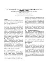
Chapter 2: Constraints from lcos technology CH2 - 45<br />
With full custom design, the layout is constructed through manual placement <strong>of</strong><br />
devices, interconnections (arrow 2). It is needless 3 to say that even <strong>for</strong> moderately<br />
complex circuits, the layout job quickly becomes tedious. Three different (Cadence)<br />
tools speed up the layout job, especially <strong>for</strong> circuits involving large amounts <strong>of</strong><br />
repetition. A first tool is the 'structure compiler’, which helps generating aligned<br />
arrays <strong>of</strong> cells through parameterization <strong>of</strong> the arrays. The second tool comes with<br />
parameterized cells – the so-called pCells. Pcells represent programmable layout<br />
blocks. The third tool is the Skill ® language interpreter that allows to access, to<br />
modify and to create data directly in the design database. Section 5.3 gives scores <strong>of</strong><br />
examples. Yet another tool is the verification s<strong>of</strong>tware; it can automatically generate<br />
some (parts <strong>of</strong>) mask layouts from the data <strong>for</strong> other masks and/or from data on extra<br />
help layers.<br />
The basis <strong>for</strong> the creation <strong>of</strong> a mask layout is the schematic circuit description. Spice<br />
netlists are systematic textual description <strong>of</strong> a circuit (arrow 1). Graphical editors<br />
like Cadence-Composer or simple text editors are used to create spice netlists. A<br />
spice circuit simulator checks the intended behavior <strong>of</strong> the schematic. At this<br />
simulation stage, it is necessary to evaluate the behavior taking into account the<br />
tolerances that exist on component values, on component models, on temperature...<br />
Moreover, eventually be<strong>for</strong>e anything can start, a sound set <strong>of</strong> technical<br />
specifications is the ultimate input to start up the whole design cycle. One last point<br />
is missing: the design cycle is used both <strong>for</strong> sub-blocks <strong>of</strong> the chip circuit as <strong>for</strong> the<br />
entire chip circuit. In other words, this cycle is repeated again and again, starting<br />
with small sub-blocks and ending with the complete chip layout.<br />
2.2 Lcos cell assembly technology highlights<br />
This section describes design restrictions imposed by the cell assembly processes.<br />
The first paragraph presents an lcos cell cross section along with the issues <strong>of</strong> spacer<br />
technology and chip planarity. The second paragraph gives a quick look at the ways<br />
reflective LC cells can be packaged and how electrical contact can be established.<br />
The last paragraph collects a set <strong>of</strong> mask design rules intended to prevent design<br />
errors that would jeopardize the yield <strong>of</strong> the panel assembly process.<br />
2.2.1 The lcos cell structure<br />
2.2.1.1 Cell cross section<br />
Cell cross sections tell a lot about the structure <strong>of</strong> lcos panels. The cross sections<br />
include cross sections <strong>of</strong> the silicon backplane; the text however must not disclose<br />
3 not the ones from the haystack<br />
CH2 - 45