RS232 DCE/DTE Sipex SP232A IC Datasheet - Solarbotics
RS232 DCE/DTE Sipex SP232A IC Datasheet - Solarbotics
RS232 DCE/DTE Sipex SP232A IC Datasheet - Solarbotics

You also want an ePaper? Increase the reach of your titles
YUMPU automatically turns print PDFs into web optimized ePapers that Google loves.
SP310A transmitter and receiver outputs in a high<br />
impedance condition (tri-stated). The shutdown<br />
mode is controlled on the SP312A by a logic “0”<br />
on the SHUTDOWN control line (pin 18); this also<br />
puts the transmitter outputs in a tri–state mode.<br />
The receiver outputs can be tri–stated separately<br />
during normal operation or shutdown by a logic<br />
“1” on the ENABLE line (pin 1).<br />
Wake–Up Feature for the SP312A<br />
The SP312A has a wake–up feature that keeps<br />
all the receivers in an enabled state when the<br />
device is in the shutdown mode. Table 1 defines<br />
the truth table for the wake–up function.<br />
With only the receivers activated, the SP312A<br />
typically draws less than 5µA supply current.<br />
In the case of a modem interfaced to a computer<br />
in power down mode, the Ring Indicator (RI)<br />
signal from the modem would be used to "wake<br />
up" the computer, allowing it to accept data<br />
transmission.<br />
After the ring indicator signal has propagated<br />
through the SP312A receiver, it can be used to<br />
trigger the power management circuitry of the<br />
computer to power up the microprocessor, and<br />
bring the SD pin of the SP312A to a logic high,<br />
taking it out of the shutdown mode. The receiver<br />
propagation delay is typically 1µs. The enable<br />
time for V + and V – is typically 2ms. After V + and<br />
V – have settled to their final values, a signal can<br />
be sent back to the modem on the data terminal<br />
ready (DTR) pin signifying that the computer is<br />
ready to accept and transmit data.<br />
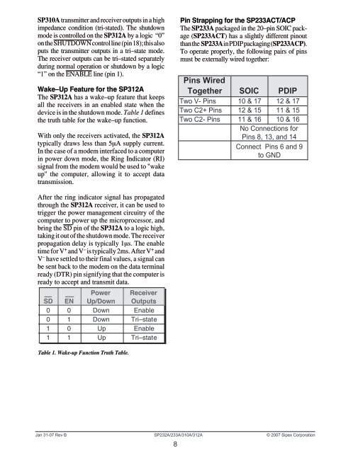
SD EN<br />
0<br />
0<br />
1<br />
1<br />
0<br />
1<br />
0<br />
1<br />
Power<br />
Up/Down<br />
Down<br />
Down<br />
Up<br />
Up<br />
Table 1. Wake-up Function Truth Table.<br />
Receiver<br />
Outputs<br />
Enable<br />
Tri–state<br />
Enable<br />
Tri–state<br />
Pin Strapping for the SP233ACT/ACP<br />
The SP233A packaged in the 20–pin SO<strong>IC</strong> package<br />
(SP233ACT) has a slightly different pinout<br />
than the SP233A in PDIP packaging (SP233ACP).<br />
To operate properly, the following pairs of pins<br />
must be externally wired together:<br />
Pins Wired<br />
Together SO<strong>IC</strong> PDIP<br />
Two V- Pins 10 & 17 12 & 17<br />
Two C2+ Pins 12 & 15 11 & 15<br />
Two C2- Pins 11 & 16 10 & 16<br />
No Connections for<br />
Pins 8, 13, and 14<br />
Connect Pins 6 and 9<br />
to GND<br />
Jan 3 -07 Rev B <strong>SP232A</strong>/233A/3 0A/3 2A © 2007 <strong>Sipex</strong> Corporation