RS232 DCE/DTE Sipex SP232A IC Datasheet - Solarbotics
RS232 DCE/DTE Sipex SP232A IC Datasheet - Solarbotics
RS232 DCE/DTE Sipex SP232A IC Datasheet - Solarbotics

You also want an ePaper? Increase the reach of your titles
YUMPU automatically turns print PDFs into web optimized ePapers that Google loves.
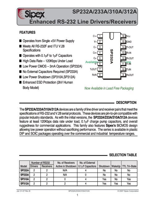
FEATURES<br />
Solved by<br />
<strong>SP232A</strong>/233A/310A/312A<br />
TM<br />
Enhanced RS-232 Line Drivers/Receivers<br />
■ Operates from Single +5V Power Supply<br />
■ Meets All RS-232F and ITU V.28<br />
Specifications<br />
■ Operates with 0.1µF to 1µF Capacitors<br />
■ High Data Rate – 120Kbps Under Load<br />
■ Low Power CMOS – 3mA Operation (<strong>SP232A</strong>)<br />
■ No External Capacitors Required (SP233A)<br />
■ Low Power Shutdown (SP310A,SP312A)<br />
■ Enhanced ESD Protection (2kV Human<br />
Body Model)<br />
C2- 5<br />
12 R1OUT<br />
Available in Lead Free Packaging<br />
V- 6<br />
11 T1IN<br />
Now Available in Lead Free Packaging<br />
DESCRIPTION<br />
The <strong>SP232A</strong>/233A/310A/312A devices are a family of line driver and receiver pairs that meet the<br />
specifications of RS-232 and V.28 serial protocols. These devices are pin-to-pin compatible with<br />
popular industry standards. As with the initial versions, the <strong>SP232A</strong>/233A/310A/312A devices<br />
feature at least 120Kbps data rate under load, 0.1µF charge pump capacitors, and overall<br />
ruggedness for commercial applications. This family also features <strong>Sipex</strong>'s BiCMOS design<br />
allowing low power operation without sacrificing performance. The series is available in plastic<br />
DIP and SO<strong>IC</strong> packages operating over the commercial and industrial temperature ranges.<br />
SELECTION TABLE<br />
Number of <strong>RS232</strong> No. of Receivers No. of External<br />
Model Drivers Receivers Active in Shutdown 0.1µF Capacitors Shutdown WakeUp TTL Tri–State<br />
<strong>SP232A</strong> 2 2 N//A 4 No No No<br />
SP233A 2 2 N/A 0 No No No<br />
SP310A 2 2 0 4 Yes No Yes<br />
SP312A 2 2 2 4 Yes Yes Yes<br />
Jan 3 -07 Rev B <strong>SP232A</strong>/233A/3 0A/3 2A © 2007 <strong>Sipex</strong> Corporation<br />
C1+<br />
V+<br />
C1-<br />
C2+<br />
T2OUT<br />
R2IN<br />
1<br />
2<br />
3<br />
4<br />
7<br />
8<br />
<strong>SP232A</strong><br />
16<br />
15<br />
14<br />
13<br />
10<br />
9<br />
VCC<br />
GND<br />
T1OUT<br />
R1IN<br />
T2IN<br />
R2OUT
This is a stress rating only and functional operation of the device at<br />
these or any other conditions above those indicated in the operation<br />
sections of this specification is not implied. Exposure to absolute<br />
maximum rating conditions for extended periods of time may affect<br />
reliability.<br />
V cc ................................................................................................................................................................. +6V<br />
V + .................................................................................................................... (Vcc-0.3V) to +11.0V<br />
V - ............................................................................................................................................................ -11.0V<br />
Input Voltages<br />
T IN ......................................................................................................................... -0.3 to (Vcc +0.3V)<br />
R IN ............................................................................................................................................................ ±30V<br />
V CC =+5V±10%; 0.1µF charge pump capacitors; T MIN to T MAX unless otherwise noted.<br />
PARAMETERS MIN. TYP. MAX. UNITS CONDITIONS<br />
TTL INPUT<br />
Logic Threshold<br />
LOW 0.8 Volts T ; EN, SD<br />
IN<br />
HIGH<br />
Logic Pull-Up Current<br />
TTL OUTPUT<br />
2.0<br />
15 200<br />
Volts<br />
µA<br />
T ; EN, SD<br />
IN<br />
T = ZeroV<br />
IN<br />
TTL/CMOS Output<br />
Voltage, Low<br />
Voltage, High 3.5<br />
0.4 Volts<br />
Volts<br />
I = 3.2mA; Vcc = +5V<br />
OUT<br />
IOUT= -1.0mA<br />
Leakage Current; T = +25 ° A<br />
RS-232 OUTPUT<br />
0.05 ±10 µA EN= V , CC ZeroVV V OUT CC<br />
SP310A and SP312A only<br />
Output Voltage Swing ±5 ±6 Volts All transmitter outputs loaded<br />
with 3kto Ground<br />
Output Resistance<br />
Output Short Circuit Current<br />
300<br />
±18<br />
Ohms<br />
mA<br />
V = CC ZeroV; V = ±2V<br />
OUT<br />
Infinite duration<br />
Maximum Data Rate<br />
RS-232 INPUT<br />
120 240 Kbps C = 2500pF, R = 3k<br />
L L<br />
Voltage Range<br />
Voltage Threshold<br />
-30 +30 Volts<br />
LOW<br />
HIGH<br />
Hysteresis<br />
Resistance<br />
0.8<br />
0.2<br />
3<br />
1.2<br />
1.7<br />
0.5<br />
5<br />
2.4<br />
1.0<br />
7<br />
Volts<br />
Volts<br />
Volts<br />
k<br />
V = 5V, T = +25 °C<br />
CC A<br />
V = 5V, T = +25 °C<br />
CC A<br />
V = 5V, T = +25 °C<br />
CC A<br />
T = +25 °C, -15V V +15V<br />
A IN<br />
DYNAM<strong>IC</strong> CHARACTERIST<strong>IC</strong>S<br />
Driver Propagation Delay<br />
Receiver Propagation Delay<br />
1.5<br />
0.1<br />
3.0<br />
1.0<br />
µs<br />
µs<br />
TTL to RS-232; C = 50pF<br />
L<br />
RS-232 to TTL<br />
Instantaneous Slew Rate<br />
Transition Region Slew Rate 10<br />
30 V/µs<br />
V/µs<br />
C = 10pF, R = 3-7k;<br />
L L<br />
T =+25 °C<br />
A<br />
C = 2500pF, R = 3k;<br />
L L<br />
measured from +3V to -3V<br />
or -3V to +3V<br />
Output Enable Time 400 ns SP310A and SP312A only<br />
Output Disable Time<br />
POWER REQUIREMENTS<br />
250 ns SP310A and SP312A only<br />
V Power Supply Current<br />
CC<br />
<strong>SP232A</strong><br />
SP233A, SP310A, SP312A<br />
3<br />
10<br />
5<br />
15<br />
mA<br />
mA<br />
No load, T = +25°C; V = 5V<br />
A CC<br />
No load, T = +25°C; V = 5V<br />
A CC<br />
V Supply Current,Loaded<br />
CC<br />
<strong>SP232A</strong> 15 mA All transmitters R = 3k ;<br />
L<br />
TA = +25 °C<br />
SP233A, SP310A, SP312A<br />
Shutdown Supply Current<br />
25 mA All transmitters R = 3k ;<br />
L<br />
T = +25 °C<br />
A<br />
SP310A,SP312A 1 10 µA V = 5V, T = +25 °C<br />
CC A<br />
Jan 3 -07 Rev B <strong>SP232A</strong>/233A/3 0A/3 2A © 2007 <strong>Sipex</strong> Corporation<br />
2<br />
ABSOLUTE MAXIMUM RATINGS<br />
Output Voltages<br />
T OUT .................................................................................................... (V+, +0.3V) to (V-, -0.3V)<br />
R OUT ................................................................................................................ -0.3V to (Vcc +0.3V)<br />
Short Circuit Duration<br />
T OUT ......................................................................................................................................... Continuous<br />
Plastic DIP .......................................................................... 375mW<br />
(derate 7mW/°C above +70°C)<br />
Small Outline ...................................................................... 375mW<br />
(derate 7mW/°C above +70°C)<br />
ELECTR<strong>IC</strong>AL CHARACTERIST<strong>IC</strong>S
V– Voltage (Volts)<br />
T 2IN<br />
T 1IN<br />
-11<br />
-10<br />
-9<br />
-8<br />
-7<br />
-6<br />
-5<br />
-4<br />
-3<br />
0 2 4 6 8 10 12 14<br />
C1+<br />
V+<br />
C1-<br />
C2+<br />
C2-<br />
V-<br />
T2OUT<br />
R2IN<br />
R 1OUT<br />
R 1IN<br />
T 1 OUT<br />
GND<br />
VCC<br />
C 1+<br />
GND<br />
C 2-<br />
1<br />
2<br />
3<br />
4<br />
5<br />
6<br />
7<br />
8<br />
9<br />
10<br />
VCC= 6V<br />
VCC= 5V<br />
VCC= 4V<br />
Load Current (mA)<br />
1<br />
2<br />
3<br />
4<br />
5<br />
6<br />
7<br />
8<br />
SP233ACP/AEP<br />
<strong>SP232A</strong><br />
20-PIN PLAST<strong>IC</strong> DIP<br />
20<br />
19<br />
18<br />
17<br />
16<br />
15<br />
14<br />
13<br />
12<br />
11<br />
V+ (Volts)<br />
12<br />
10<br />
8<br />
6<br />
4<br />
2<br />
VCC= 6V<br />
VCC= 5V<br />
VCC= 4V<br />
0<br />
0 5 10 15 20 25 30 35 40<br />
16<br />
15<br />
14<br />
13<br />
12<br />
11<br />
10<br />
9<br />
R OUT<br />
2<br />
R 2IN<br />
T 2OUT<br />
V-<br />
C 2 -<br />
C 2+<br />
V+<br />
C 1 -<br />
V-<br />
C 2 +<br />
Load Current (mA)<br />
VCC<br />
GND<br />
T1OUT<br />
R1IN<br />
R1OUT<br />
T1IN<br />
T2IN<br />
R2OUT<br />
NC *<br />
C1+<br />
V+<br />
C1-<br />
C2+<br />
C2-<br />
V-<br />
T2OUT<br />
R2IN<br />
1<br />
2<br />
3<br />
4<br />
5<br />
6<br />
7<br />
8<br />
9<br />
SP310A<br />
Jan 3 -07 Rev B <strong>SP232A</strong>/233A/3 0A/3 2A © 2007 <strong>Sipex</strong> Corporation<br />
3<br />
Not 100% tested.<br />
<strong>IC</strong>C (mA)<br />
30<br />
25<br />
20<br />
15<br />
10<br />
5<br />
VCC= 6V<br />
VCC= 5V<br />
VCC= 4V<br />
VCC= 3V<br />
0<br />
-55 -40 0 25 70 85 125<br />
T2IN<br />
T1IN<br />
R1OUT<br />
R1IN<br />
T1OUT<br />
GND<br />
VCC<br />
V+ DNC<br />
GND<br />
Conn to 17<br />
18<br />
17<br />
16<br />
15<br />
14<br />
13<br />
12<br />
11<br />
10<br />
Temperature (°C)<br />
1<br />
2<br />
3<br />
4<br />
5<br />
6<br />
7<br />
8<br />
9<br />
10<br />
ON/OFF<br />
VCC<br />
GND<br />
T1OUT<br />
R1IN<br />
R1OUT<br />
T1IN<br />
T2IN<br />
R2OUT<br />
PERFORMANCE CURVES<br />
SP233ACT/AET<br />
VOH (Volts)<br />
9.0<br />
8.5<br />
8.0<br />
7.5<br />
7.0<br />
6.5<br />
6.0<br />
5.5<br />
20-PIN SO<strong>IC</strong><br />
See Figure 2 for<br />
Pin Connections<br />
EN *<br />
C1+<br />
V+<br />
C1-<br />
C2+<br />
C2-<br />
V-<br />
T2OUT<br />
R2IN<br />
1<br />
2<br />
3<br />
4<br />
5<br />
6<br />
7<br />
8<br />
9<br />
Load current = 0mA<br />
TA= 25 °C<br />
5.0<br />
4.5 4.75 5.0 5.25 5.5<br />
SP312A<br />
20<br />
19<br />
18<br />
17<br />
16<br />
15<br />
14<br />
13<br />
12<br />
11<br />
VCC(Volts)<br />
PINOUTS<br />
R2OUT<br />
R2IN<br />
T2OUT<br />
Conn to 10<br />
Conn to 11<br />
Conn to 12<br />
C1- DNC<br />
C1+ DNC<br />
Conn to 15<br />
Conn to 16<br />
18<br />
17<br />
16<br />
15<br />
14<br />
13<br />
12<br />
11<br />
10<br />
SHUTDOWN<br />
VCC<br />
GND<br />
T1OUT<br />
R1IN<br />
R1OUT<br />
T1IN<br />
T2IN<br />
R2OUT<br />
* N.C. for SP310E_A, EN for SP312E_A
FEATURES…<br />
The <strong>SP232A</strong>/233A/310A/312A devices are a<br />
family of line driver and receiver pairs that meet<br />
the specifications of RS-232 and V.28 serial<br />
protocols. The ESD tolerance has been improved<br />
on these devices to over ±2KV for the<br />
Human Body Model. These devices are pin-topin<br />
compatible with popular industry standards.<br />
The <strong>SP232A</strong>/233A/310A/312A devices<br />
feature10V/µs slew rate, 120Kbps data rate under<br />
load, 0.1µF charge pump capacitors, overall<br />
ruggedness for commercial applications, and<br />
increased drive current for longer and more<br />
flexible cable configurations. This family also<br />
features <strong>Sipex</strong>'s BiCMOS design allowing low<br />
power operation without sacrificing performance.<br />
The <strong>SP232A</strong>/233A/310A/312A devices have<br />
internal charge pump voltage converters which<br />
allow them to operate from a single +5V supply.<br />
The charge pumps will operate with polarized or<br />
non-polarized capacitors ranging from 0.1 to 1µF<br />
and will generate the ±6V needed for the RS-<br />
232 output levels. Both meet all EIA RS-232F<br />
and ITU V.28 specifications.<br />
TTL/CMOS OUTPUTS<br />
TTL/CMOS INPUTS<br />
T IN<br />
1<br />
T IN<br />
2<br />
R OUT<br />
1<br />
R OUT<br />
2<br />
Figure 1. Typical Circuit using the <strong>SP232A</strong>.<br />
1<br />
0.1 µ F + C +<br />
1<br />
6.3V 3<br />
4<br />
C 1-<br />
0.1 µ F + C +<br />
2<br />
10V 5 C 2-<br />
10 µ F 6.3V<br />
+<br />
+5V INPUT<br />
400k <br />
11 14<br />
T1 400k <br />
16<br />
V CC<br />
Charge Pump<br />
10 7<br />
T2 12 13<br />
R1 9 8<br />
R2 <strong>SP232A</strong><br />
GND 15<br />
The SP310A provides identical features as the<br />
<strong>SP232A</strong> with the addition of a single control<br />
line which simultaneously shuts down the internal<br />
DC/DC converter and puts all transmitter<br />
and receiver outputs into a high impedance<br />
state. The SP312A is identical to the SP310A<br />
with separate tri-state and shutdown control<br />
lines.<br />
THEORY OF OPERATION<br />
The <strong>SP232A</strong>, SP233A, SP310A and SP312A<br />
devices are made up of three basic circuit blocks –<br />
1) a driver/transmitter, 2) a receiver and 3) a charge<br />
pump. Each block is described below.<br />
Driver/Transmitter<br />
The drivers are inverting transmitters, which accept<br />
TTL or CMOS inputs and output the RS-232<br />
signals with an inverted sense relative to the input<br />
logic levels. Typically the RS-232output voltage<br />
swing is ±6V. Even under worst case loading<br />
conditions of 3kOhms and 2500pF, the output is<br />
guaranteed to be ±5V, which is consistent with the<br />
RS-232 standard specifications. The transmitter<br />
outputs are protected against infinite short-circuits<br />
to ground without degradation in reliability.<br />
Jan 3 -07 Rev B <strong>SP232A</strong>/233A/3 0A/3 2A © 2007 <strong>Sipex</strong> Corporation<br />
5k<br />
5k<br />
V+<br />
V-<br />
0.1 µ F 6.3V<br />
2<br />
6<br />
+<br />
0.1 µ F<br />
10V<br />
T OUT<br />
1<br />
T OUT<br />
2<br />
R IN<br />
1<br />
R IN<br />
2<br />
*The negative terminal of the V+ storage capacitor can be tied<br />
to either V CC or GND. Connecting the capacitor to V CC (+5V)<br />
is recommended.<br />
+<br />
*<br />
RS-232 INPUTS<br />
RS-232 OUTPUTS
TTL/CMOS OUTPUTS<br />
TTL/CMOS INPUTS<br />
T IN<br />
1<br />
T IN<br />
2<br />
R OUT<br />
1<br />
R OUT<br />
2<br />
Do not make<br />
connection to<br />
these pins<br />
+5V INPUT<br />
2 400k <br />
5<br />
T1 1 400k <br />
18<br />
T2 3 4<br />
R1 20 19<br />
R2 8<br />
C +<br />
1<br />
5k<br />
13<br />
C 1-<br />
C + 11<br />
2<br />
14<br />
V+<br />
C +<br />
15<br />
2<br />
12 V-<br />
17 V-<br />
SP233ACP<br />
GND GND<br />
10<br />
C 2 -<br />
16<br />
C 2 -<br />
6<br />
T OUT<br />
1<br />
T OUT<br />
2<br />
R IN<br />
1<br />
R IN<br />
2<br />
Figure 2. Typical Circuits using the SP233ACP and SP233ACT<br />
The instantaneous slew rate of the transmitter<br />
output is internally limited to a maximum of 30V/<br />
µs in order to meet the standards [EIA RS-232-F ].<br />
The transition region slew rate of these enhanced<br />
products is typically 10V/µs. The smooth transition<br />
of the loaded output from V OL to V OH clearly<br />
meets the monotonicity requirements of the standard<br />
[EIA RS-232-F].<br />
Receivers<br />
The receivers convert RS-232 input signals to<br />
inverted TTL signals. Since the input is usually<br />
from a transmission line, where long cable lengths<br />
and system interference can degrade the signal, the<br />
TTL/CMOS OUTPUTS<br />
TTL/CMOS INPUTS<br />
2<br />
0.1 µ F + C +<br />
1<br />
6.3V 4<br />
5<br />
C 1-<br />
0.1 µ F + C +<br />
2<br />
16V 6 C 2-<br />
T IN<br />
1<br />
T IN<br />
2<br />
R OUT<br />
1<br />
R OUT<br />
2<br />
10 µ F 6.3V<br />
+<br />
400k <br />
Figure 3. Typical Circuits using the SP310A and SP312A<br />
7<br />
V CC<br />
+5V INPUT<br />
5k<br />
12 15<br />
T1 400k <br />
17<br />
V CC<br />
Charge Pump<br />
11 8<br />
T2 13 14<br />
R1 10 9<br />
R2 SP310A<br />
GND 16<br />
5k<br />
5k<br />
9<br />
0.1 µF<br />
10V<br />
3<br />
V+ +<br />
7<br />
V-<br />
18<br />
+<br />
RS-232 INPUTS<br />
RS-232 OUTPUTS<br />
Connect on PCB<br />
Pin 11 to Pin 15<br />
Pin 10 to Pin 16<br />
Pin 12 to Pin 17<br />
Both Pins 6 and 9 to GND<br />
T OUT<br />
1<br />
T OUT<br />
2<br />
R IN<br />
1<br />
R IN<br />
2<br />
*<br />
0.1 µF<br />
10V<br />
ON/OFF<br />
*The negative terminal of the V+ storage capacitor can be tied<br />
to either V CC or GND. Connecting the capacitor to V CC (+5V)<br />
is recommended.<br />
RS-232 INPUTS<br />
RS-232 OUTPUTS<br />
20 19<br />
R2 inputs have a typical hysteresis margin of 500mV.<br />
This ensures that the receiver is virtually immune<br />
to noisy transmission lines.<br />
The input thresholds are 0.8V minimum and 2.4V<br />
maximum, again well within the ±3V RS-232<br />
requirements. The receiver inputs are also protected<br />
against voltages up to ±25V. Should an<br />
input be left unconnected, a 5K pulldown resistor<br />
to ground will commit the output of the receiver<br />
to a high state.<br />
Jan 3 -07 Rev B <strong>SP232A</strong>/233A/3 0A/3 2A © 2007 <strong>Sipex</strong> Corporation<br />
TTL/CMOS OUTPUTS<br />
TTL/CMOS INPUTS<br />
TTL/CMOS OUTPUTS<br />
TTL/CMOS INPUTS<br />
R OUT<br />
1<br />
R OUT<br />
2<br />
T IN<br />
1<br />
T IN<br />
2<br />
R OUT<br />
1<br />
R OUT<br />
2<br />
Do not make<br />
connection to<br />
these pins<br />
T IN<br />
1<br />
T IN<br />
2<br />
13<br />
10<br />
+5V INPUT<br />
2 400k <br />
5<br />
T1 1 400k <br />
18<br />
T2 3 4<br />
R1 13<br />
C +<br />
1<br />
5k<br />
14<br />
C 1-<br />
C + 12<br />
2<br />
8<br />
V+<br />
C +<br />
15<br />
2<br />
10<br />
V-<br />
17<br />
V-<br />
SP233ACT<br />
GND GND<br />
11<br />
C 2 -<br />
16<br />
C 2 -<br />
400k <br />
R 1<br />
R 2<br />
6<br />
+5V INPUT<br />
7<br />
V CC<br />
5k<br />
17<br />
2<br />
0.1 µ F<br />
C + V 10V<br />
1<br />
CC<br />
0.1 µ F +<br />
3<br />
V+ +<br />
6.3V<br />
*<br />
4 C 1-<br />
5 Charge Pump<br />
C +<br />
0.1 µ F + 2<br />
7<br />
V- + 0.1 µ F<br />
16V<br />
10V<br />
6 C 2-<br />
EN<br />
12 15<br />
T1 400k <br />
11 8<br />
T2 1<br />
10 µ F 6.3V<br />
+<br />
SP312A<br />
GND 16<br />
5k<br />
5k<br />
9<br />
14<br />
9<br />
T OUT<br />
1<br />
T OUT<br />
2<br />
R IN<br />
1<br />
R IN<br />
2<br />
*The negative terminal of the V+ storage capacitor can be tied<br />
to either V CCor GND. Connecting the capacitor to V CC(+5V)<br />
is recommended.<br />
18<br />
T OUT<br />
1<br />
T OUT<br />
2<br />
R IN<br />
1<br />
R IN<br />
2<br />
RS-232 INPUTS<br />
RS-232 OUTPUTS<br />
Connect on PCB<br />
Pin 12 to Pin 15<br />
Pin 11 to Pin 16<br />
Pin 10 to Pin 17<br />
Both Pins 6 and 9 to GND<br />
RS-232 INPUTS<br />
RS-232 OUTPUTS<br />
SHUTDOWN
Figure 4. Charge Pump — Phase 1<br />
In actual system applications, it is quite possible<br />
for signals to be applied to the receiver inputs<br />
before power is applied to the receiver circuitry.<br />
This occurs, for example, when a PC user attempts<br />
to print, only to realize the printer wasn’t turned on.<br />
In this case an RS-232 signal from the PC will<br />
appear on the receiver input at the printer. When<br />
the printer power is turned on, the receiver will<br />
operate normally. All of these enhanced devices<br />
are fully protected.<br />
Charge Pump<br />
The charge pump is a <strong>Sipex</strong>–patented design<br />
(5,306,954) and uses a unique approach compared<br />
to older less–efficient designs. The charge<br />
pump still requires four external capacitors, but<br />
uses a four–phase voltage shifting technique to<br />
attain symmetrical power supplies. There is a<br />
free–running oscillator that controls the four<br />
phases of the voltage shifting. A description of<br />
each phase follows.<br />
Phase 1<br />
— V SS charge storage —During this phase of<br />
the clock cycle, the positive side of capacitors<br />
C 1 and C 2 are initially charged to +5V. C l + is<br />
then switched to ground and the charge in C 1 – is<br />
transferred to C 2 – . Since C2 + is connected to<br />
+5V, the voltage potential across capacitor C 2 is<br />
now 10V.<br />
Figure 5. Charge Pump — Phase 2<br />
V CC = +5V<br />
+ +<br />
C1 C<br />
–<br />
2<br />
–<br />
–Vcc<br />
V CC= +5V<br />
+Vcc<br />
–Vcc<br />
+ +<br />
C1 C<br />
–<br />
2<br />
–<br />
Vss<br />
V DDStorage Capacitor (V+)<br />
V SS Storage Capacitor (V-)<br />
Phase 2<br />
— V SS transfer — Phase two of the clock connects<br />
the negative terminal of C 2 to the V SS<br />
storage capacitor and the positive terminal of C 2<br />
to ground, and transfers the generated –l0V to<br />
C 3 . Simultaneously, the positive side of capacitor<br />
C 1 is switched to +5V and the negative side<br />
is connected to ground.<br />
Phase 3<br />
— V DD charge storage — The third phase of the<br />
clock is identical to the first phase — the charge<br />
transferred in C 1 produces –5V in the negative<br />
terminal of C 1 , which is applied to the negative<br />
side of capacitor C 2 . Since C 2 + is at +5V, the<br />
voltage potential across C 2 is a maximum of l0V.<br />
Phase 4<br />
— V DD transfer — The fourth phase of the clock<br />
connects the negative terminal of C 2 to ground,<br />
and transfers the generated l0V across C 2 to C 4 ,<br />
the V DD storage capacitor. Again, simultaneously<br />
with this, the positive side of capacitor C 1 is<br />
switched to +5V and the negative side is connected<br />
to ground, and the cycle begins again.<br />
Since both V + and V – are separately generated<br />
from V CC ; in a no–load condition V + and V – will<br />
be symmetrical. Older charge pump approaches<br />
Jan 3 -07 Rev B <strong>SP232A</strong>/233A/3 0A/3 2A © 2007 <strong>Sipex</strong> Corporation<br />
C 4<br />
+<br />
–<br />
+<br />
C 3<br />
–<br />
C 4<br />
+<br />
–<br />
–<br />
+<br />
C 3<br />
V DDStorage Capacitor<br />
V SSStorage Capacitor
+ a) C2 – b) C2 VDD<br />
GND<br />
GND<br />
Vss<br />
Figure 6. Charge Pump Waveforms<br />
that generate V – from V + will show a decrease in<br />
the magnitude of V – compared to V + due to the<br />
inherent inefficiencies in the design.<br />
The clock rate for the charge pump typically<br />
operates at greater than 15kHz. The external<br />
capacitors can be as low as 0.1µF with a 10V<br />
breakdown voltage rating.<br />
–5V<br />
Figure 7. Charge Pump — Phase 3<br />
Figure 8. Charge Pump — Phase 4<br />
V CC= +5V<br />
+5V<br />
+ +<br />
C1 C<br />
–<br />
2<br />
–<br />
Vcc = +5V<br />
–5V<br />
VDD<br />
+ +<br />
C1 C<br />
–<br />
2<br />
–<br />
Jan 3 -07 Rev B <strong>SP232A</strong>/233A/3 0A/3 2A © 2007 <strong>Sipex</strong> Corporation<br />
7<br />
Shutdown (SD) and Enable (EN) for the<br />
SP310A and SP312A<br />
Both the SP310A and SP312A have a shutdown/<br />
standby mode to conserve power in battery-powered<br />
systems. To activate the shutdown mode,<br />
which stops the operation of the charge pump, a<br />
logic “0” is applied to the appropriate control line.<br />
For the SP310A, this control line is ON/OFF (pin<br />
18). Activating the shutdown mode also puts the<br />
C 4<br />
+<br />
–<br />
+<br />
C 3<br />
–<br />
C 4<br />
+<br />
–<br />
V DD Storage Capacitor<br />
V SS Storage Capacitor<br />
–<br />
+<br />
C 3<br />
V DDStorage Capacitor<br />
V SSStorage Capacitor
SP310A transmitter and receiver outputs in a high<br />
impedance condition (tri-stated). The shutdown<br />
mode is controlled on the SP312A by a logic “0”<br />
on the SHUTDOWN control line (pin 18); this also<br />
puts the transmitter outputs in a tri–state mode.<br />
The receiver outputs can be tri–stated separately<br />
during normal operation or shutdown by a logic<br />
“1” on the ENABLE line (pin 1).<br />
Wake–Up Feature for the SP312A<br />
The SP312A has a wake–up feature that keeps<br />
all the receivers in an enabled state when the<br />
device is in the shutdown mode. Table 1 defines<br />
the truth table for the wake–up function.<br />
With only the receivers activated, the SP312A<br />
typically draws less than 5µA supply current.<br />
In the case of a modem interfaced to a computer<br />
in power down mode, the Ring Indicator (RI)<br />
signal from the modem would be used to "wake<br />
up" the computer, allowing it to accept data<br />
transmission.<br />
After the ring indicator signal has propagated<br />
through the SP312A receiver, it can be used to<br />
trigger the power management circuitry of the<br />
computer to power up the microprocessor, and<br />
bring the SD pin of the SP312A to a logic high,<br />
taking it out of the shutdown mode. The receiver<br />
propagation delay is typically 1µs. The enable<br />
time for V + and V – is typically 2ms. After V + and<br />
V – have settled to their final values, a signal can<br />
be sent back to the modem on the data terminal<br />
ready (DTR) pin signifying that the computer is<br />
ready to accept and transmit data.<br />
SD EN<br />
0<br />
0<br />
1<br />
1<br />
0<br />
1<br />
0<br />
1<br />
Power<br />
Up/Down<br />
Down<br />
Down<br />
Up<br />
Up<br />
Table 1. Wake-up Function Truth Table.<br />
Receiver<br />
Outputs<br />
Enable<br />
Tri–state<br />
Enable<br />
Tri–state<br />
Pin Strapping for the SP233ACT/ACP<br />
The SP233A packaged in the 20–pin SO<strong>IC</strong> package<br />
(SP233ACT) has a slightly different pinout<br />
than the SP233A in PDIP packaging (SP233ACP).<br />
To operate properly, the following pairs of pins<br />
must be externally wired together:<br />
Pins Wired<br />
Together SO<strong>IC</strong> PDIP<br />
Two V- Pins 10 & 17 12 & 17<br />
Two C2+ Pins 12 & 15 11 & 15<br />
Two C2- Pins 11 & 16 10 & 16<br />
No Connections for<br />
Pins 8, 13, and 14<br />
Connect Pins 6 and 9<br />
to GND<br />
Jan 3 -07 Rev B <strong>SP232A</strong>/233A/3 0A/3 2A © 2007 <strong>Sipex</strong> Corporation
PAckAgE: 16 Pin nSoic<br />
Jan 3 -07 Rev B <strong>SP232A</strong>/233A/3 0A/3 2A © 2007 <strong>Sipex</strong> Corporation
Jan 3 -07 Rev B <strong>SP232A</strong>/233A/3 0A/3 2A © 2007 <strong>Sipex</strong> Corporation<br />
0<br />
PAckAgE: 16 Pin WSoic
PAckAgE: 18 Pin WSoic<br />
Jan 3 -07 Rev B <strong>SP232A</strong>/233A/3 0A/3 2A © 2007 <strong>Sipex</strong> Corporation
Jan 3 -07 Rev B <strong>SP232A</strong>/233A/3 0A/3 2A © 2007 <strong>Sipex</strong> Corporation<br />
2<br />
PAckAgE: 20 Pin WSoic
Jan 3 -07 Rev B <strong>SP232A</strong>/233A/3 0A/3 2A © 2007 <strong>Sipex</strong> Corporation<br />
3<br />
PAckAgE: 16 Pin PDiP
PAckAgE: 18 Pin PDiP<br />
Jan 3 -07 Rev B <strong>SP232A</strong>/233A/3 0A/3 2A © 2007 <strong>Sipex</strong> Corporation
PAckAgE: 20 Pin PDiP<br />
Jan 3 -07 Rev B <strong>SP232A</strong>/233A/3 0A/3 2A © 2007 <strong>Sipex</strong> Corporation
Part Number Temperature Range Topmark Package<br />
<strong>SP232A</strong>CN.............................0°C to +70°C................................<strong>SP232A</strong>CN..........................................................................16–pin NSO<strong>IC</strong><br />
<strong>SP232A</strong>CN/TR.......................0°C to +70°C................................<strong>SP232A</strong>CN..........................................................................16–pin NSO<strong>IC</strong><br />
<strong>SP232A</strong>CP.............................0°C to +70°C.................................<strong>SP232A</strong>CP.........................................................................16–pin PDIP<br />
<strong>SP232A</strong>CT.............................0°C to +70°C.................................<strong>SP232A</strong>CT..........................................................................16–pin WSO<strong>IC</strong><br />
<strong>SP232A</strong>CT/TR.......................0°C to +70°C.................................<strong>SP232A</strong>CT..........................................................................16–pin WSO<strong>IC</strong><br />
<strong>SP232A</strong>EN..........................–40°C to +85°C................................<strong>SP232A</strong>EN..........................................................................16–pin NSO<strong>IC</strong><br />
<strong>SP232A</strong>EN/TR....................–40°C to +85°C................................<strong>SP232A</strong>EN..........................................................................16–pin NSO<strong>IC</strong><br />
<strong>SP232A</strong>EP..........................–40°C to +85°C................................<strong>SP232A</strong>EP..........................................................................16–pin PDIP<br />
<strong>SP232A</strong>ET..........................–40°C to +85°C................................<strong>SP232A</strong>ET...........................................................................16–pin WSO<strong>IC</strong><br />
<strong>SP232A</strong>ET/TR.....................–40°C to +85°C................................<strong>SP232A</strong>ET...........................................................................16–pin WSO<strong>IC</strong><br />
SP233ACP.............................0°C to +70°C.................................<strong>SP232A</strong>CP.........................................................................20–pin PDIP<br />
SP233ACT............................0°C to +70°C.................................SP233ACT...........................................................................20–pin WSO<strong>IC</strong><br />
SP233ACT/TR......................0°C to +70°C.................................SP233ACT...........................................................................20–pin WSO<strong>IC</strong><br />
SP233AEP..........................–40°C to +85°C................................<strong>SP232A</strong>EP..........................................................................20–pin PDIP<br />
SP233AET..........................–40°C to +85°C................................SP233AET...........................................................................20–pin WSO<strong>IC</strong><br />
SP233AET/TR.....................–40°C to +85°C................................SP233AET...........................................................................20–pin WSO<strong>IC</strong><br />
SP310ACP............................0°C to +70°C.................................SP310ACP.........................................................................18–pin PDIP<br />
SP310ACT............................0°C to +70°C.................................SP310ACT..........................................................................18–pin WSO<strong>IC</strong><br />
SP310ACT/TR......................0°C to +70°C.................................SP310ACT..........................................................................18–pin WSO<strong>IC</strong><br />
SP310AEP..........................–40°C to +85°C................................SP310AEP..........................................................................18–pin PDIP<br />
SP310AET..........................–40°C to +85°C................................SP310AET...........................................................................18–pin WSO<strong>IC</strong><br />
SP310AET/TR.....................–40°C to +85°C................................SP310AET...........................................................................18–pin WSO<strong>IC</strong><br />
SP312ACP............................0°C to +70°C.................................SP312ACP..........................................................................18–pin PDIP<br />
SP312ACT............................0°C to +70°C.................................SP312ACT...........................................................................18–pin WSO<strong>IC</strong><br />
SP312ACT/TR......................0°C to +70°C.................................SP312ACT...........................................................................18–pin WSO<strong>IC</strong><br />
SP312AEP..........................–40°C to +85°C................................SP312AEP...........................................................................18–pin PDIP<br />
SP312AET..........................–40°C to +85°C................................SP312AET............................................................................18–pin WSO<strong>IC</strong><br />
SP312AET/TR.....................–40°C to +85°C................................SP312AET............................................................................18–pin WSO<strong>IC</strong><br />
Solved by <strong>Sipex</strong>tm<br />
Available in lead free packaging. To order add "-L" suffix to part number.<br />
Example: SP312AEA/TR = standard; SP312AEA-L/TR = lead free.<br />
/TR = Tape and Reel<br />
Pack quantity is 1,500 for WSO<strong>IC</strong> and 2,500 for NSO<strong>IC</strong>.<br />
Solved by<br />
TM<br />
<strong>Sipex</strong> corporation<br />
Headquarters and<br />
Sales Office<br />
233 South Hillview Drive<br />
Milpitas, CA 03<br />
TEL: ( 0 ) 3 -7 00<br />
FAX: ( 0 ) 3 -7 00<br />
ORDERING INFORMATION<br />
<strong>Sipex</strong> Corporation reserves the right to make changes to any products described herein. <strong>Sipex</strong> does not assume<br />
any liability arising out of the application or use of any product or circuit described herein; neither does it convey<br />
any license under its patent rights nor the rights of others.<br />
Jan 3 -07 Rev B <strong>SP232A</strong>/233A/3 0A/3 2A © 2007 <strong>Sipex</strong> Corporation