"4-Bit Binary Fill Adder With Fast Carry"
"4-Bit Binary Fill Adder With Fast Carry"
"4-Bit Binary Fill Adder With Fast Carry"

You also want an ePaper? Increase the reach of your titles
YUMPU automatically turns print PDFs into web optimized ePapers that Google loves.
Data sheet acquired from Harris Semiconductor<br />
SCHS251D<br />
August 1998 - Revised May 2000<br />
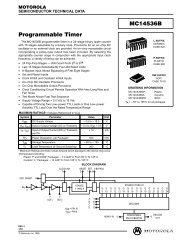
Features<br />
• Buffered Inputs<br />
• Exceeds 2kV ESD Protection MIL-STD-883, Method<br />
3015<br />
• SCR-Latchup-Resistant CMOS Process and Circuit<br />
Design<br />
• Speed of Bipolar FAST/AS/S with Significantly<br />
Reduced Power Consumption<br />
• Balanced Propagation Delays<br />
• AC Types Feature 1.5V to 5.5V Operation and<br />
Balanced Noise Immunity at 30% of the Supply<br />
• ±24mA Output Drive Current<br />
- Fanout to 15 FAST ICs<br />
- Drives 50Ω Transmission Lines<br />
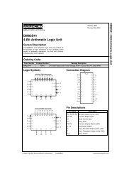
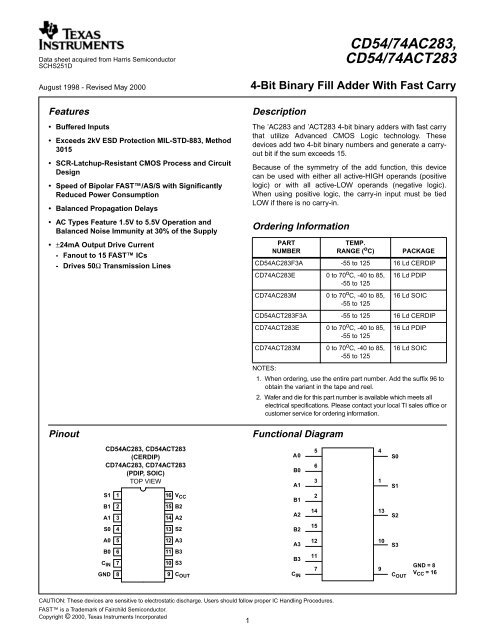
Pinout<br />
CD54AC283, CD54ACT283<br />
(CERDIP)<br />
CD74AC283, CD74ACT283<br />
(PDIP, SOIC)<br />
TOP VIEW<br />
S1<br />
B1<br />
A1<br />
S0<br />
A0<br />
B0<br />
C IN<br />
GND<br />
1<br />
2<br />
3<br />
4<br />
5<br />
6<br />
7<br />
8<br />
16 VCC 15 B2<br />
14 A2<br />
13 S2<br />
12 A3<br />
11 B3<br />
10 S3<br />
9 COUT Description<br />
The ’AC283 and ’ACT283 4-bit binary adders with fast carry<br />
that utilize Advanced CMOS Logic technology. These<br />
devices add two 4-bit binary numbers and generate a carryout<br />
bit if the sum exceeds 15.<br />
Because of the symmetry of the add function, this device<br />
can be used with either all active-HIGH operands (positive<br />
logic) or with all active-LOW operands (negative logic).<br />
When using positive logic, the carry-in input must be tied<br />
LOW if there is no carry-in.<br />
Ordering Information<br />
PART<br />
NUMBER<br />
Functional Diagram<br />
TEMP.<br />
RANGE ( o C) PACKAGE<br />
CD54AC283F3A -55 to 125 16 Ld CERDIP<br />
CD74AC283E 0 to 70oC, -40 to 85,<br />
-55 to 125<br />
16 Ld PDIP<br />
CD74AC283M 0 to 70 o C, -40 to 85,<br />
-55 to 125<br />
16 Ld SOIC<br />
CD54ACT283F3A -55 to 125 16 Ld CERDIP<br />
CD74ACT283E 0 to 70oC, -40 to 85,<br />
-55 to 125<br />
16 Ld PDIP<br />
CD74ACT283M 0 to 70 o C, -40 to 85,<br />
-55 to 125<br />
CAUTION: These devices are sensitive to electrostatic discharge. Users should follow proper IC Handling Procedures.<br />
FAST is a Trademark of Fairchild Semiconductor.<br />
Copyright © 2000, Texas Instruments Incorporated<br />
1<br />
16 Ld SOIC<br />
NOTES:<br />
1. When ordering, use the entire part number. Add the suffix 96 to<br />
obtain the variant in the tape and reel.<br />
2. Wafer and die for this part number is available which meets all<br />
electrical specifications. Please contact your local TI sales office or<br />
customer service for ordering information.<br />
A0<br />
B0<br />
A1<br />
B1<br />
A2<br />
B2<br />
A3<br />
B3<br />
C IN<br />
5<br />
6<br />
3<br />
2<br />
14<br />
15<br />
12<br />
11<br />
7<br />
CD54/74AC283,<br />
CD54/74ACT283<br />
4-<strong>Bit</strong> <strong>Binary</strong> <strong>Fill</strong> <strong>Adder</strong> <strong>With</strong> <strong>Fast</strong> Carry<br />
4<br />
1<br />
13<br />
10<br />
9<br />
S0<br />
S1<br />
S2<br />
S3<br />
C OUT<br />
GND = 8<br />
V CC = 16
Absolute Maximum Ratings Thermal Information<br />
DC Supply Voltage, V CC . . . . . . . . . . . . . . . . . . . . . . . . -0.5V to 6V<br />
DC Input Diode Current, I IK<br />
For V I < -0.5V or V I > V CC + 0.5V . . . . . . . . . . . . . . . . . . . . . .±20mA<br />
DC Output Diode Current, I OK<br />
For V O < -0.5V or V O > V CC + 0.5V . . . . . . . . . . . . . . . . . . . .±50mA<br />
DC Output Source or Sink Current per Output Pin, I O<br />
For V O > -0.5V or V O < V CC + 0.5V . . . . . . . . . . . . . . . . . . . .±50mA<br />
DC V CC or Ground Current, I CC or I GND (Note 3) . . . . . . . . .±100mA<br />
Operating Conditions<br />
Temperature Range, T A . . . . . . . . . . . . . . . . . . . . . . -55 o C to 125 o C<br />
Supply Voltage Range, V CC (Note 4)<br />
AC Types. . . . . . . . . . . . . . . . . . . . . . . . . . . . . . . . . . .1.5V to 5.5V<br />
ACT Types . . . . . . . . . . . . . . . . . . . . . . . . . . . . . . . . .4.5V to 5.5V<br />
DC Input or Output Voltage, V I , V O . . . . . . . . . . . . . . . . . 0V to V CC<br />
Input Rise and Fall Slew Rate, dt/dv<br />
AC Types, 1.5V to 3V . . . . . . . . . . . . . . . . . . . . . . . . . 50ns (Max)<br />
AC Types, 3.6V to 5.5V. . . . . . . . . . . . . . . . . . . . . . . . 20ns (Max)<br />
ACT Types, 4.5V to 5.5V. . . . . . . . . . . . . . . . . . . . . . . 10ns (Max)<br />
2<br />
Thermal Impedance (Typical, Note 5) θJA ( oC/W) PDIP Package . . . . . . . . . . . . . . . . . . . . . . . . . . . . . 67oC/W SOIC Package . . . . . . . . . . . . . . . . . . . . . . . . . . . . . 73oC/W Maximum Junction Temperature (Plastic Package) . . . . . . . . . . 150oC Maximum Storage Temperature Range . . . . . . . . . .-65oC to 150oC Maximum Lead Temperature (Soldering 10s) . . . . . . . . . . . . . 300oC CAUTION: Stresses above those listed in “Absolute Maximum Ratings” may cause permanent damage to the device. This is a stress only rating and operation<br />
of the device at these or any other conditions above those indicated in the operational sections of this specification is not implied.<br />
NOTES:<br />
3. For up to 4 outputs per device, add ±25mA for each additional output.<br />
4. Unless otherwise specified, all voltages are referenced to ground.<br />
5. The package thermal impedance is calculated in accordance with JESD 51.<br />
DC Electrical Specifications<br />
CD54/74AC283, CD54/74ACT283<br />
TEST<br />
CONDITIONS<br />
VCC 25<br />
PARAMETER SYMBOL<br />
(V)<br />
o C<br />
-40 o C TO<br />
85 o C<br />
-55 o C TO<br />
125 o C<br />
AC TYPES<br />
VI (V) IO (mA) MIN MAX MIN MAX MIN MAX UNITS<br />
High Level Input Voltage VIH - - 1.5 1.2 - 1.2 - 1.2 - V<br />
3 2.1 - 2.1 - 2.1 - V<br />
5.5 3.85 - 3.85 - 3.85 - V<br />
Low Level Input Voltage VIL - - 1.5 - 0.3 - 0.3 - 0.3 V<br />
3 - 0.9 - 0.9 - 0.9 V<br />
5.5 - 1.65 - 1.65 - 1.65 V<br />
High Level Output Voltage VOH VIH or VIL -0.05 1.5 1.4 - 1.4 - 1.4 - V<br />
-0.05 3 2.9 - 2.9 - 2.9 - V<br />
-0.05 4.5 4.4 - 4.4 - 4.4 - V<br />
-4 3 2.58 - 2.48 - 2.4 - V<br />
-24 4.5 3.94 - 3.8 - 3.7 - V<br />
-75<br />
(Note 6, 7)<br />
5.5 - - 3.85 - - - V<br />
-50<br />
(Note 6, 7)<br />
5.5 - - - - 3.85 - V
DC Electrical Specifications (Continued)<br />
TEST<br />
CONDITIONS<br />
VCC 25<br />
PARAMETER SYMBOL<br />
(V)<br />
Low Level Output Voltage VOL VIH or VIL 0.05 1.5 - 0.1 - 0.1 - 0.1 V<br />
0.05 3 - 0.1 - 0.1 - 0.1 V<br />
0.05 4.5 - 0.1 - 0.1 - 0.1 V<br />
12 3 - 0.36 - 0.44 - 0.5 V<br />
24 4.5 - 0.36 - 0.44 - 0.5 V<br />
75<br />
(Note 6, 7)<br />
5.5 - - - 1.65 - - V<br />
50<br />
(Note 6, 7)<br />
5.5 - - - - - 1.65 V<br />
Input Leakage Current II VCC or<br />
GND<br />
- 5.5 - ±0.1 - ±1 - ±1 μA<br />
Quiescent Supply Current ICC VCC or 0 5.5 - 8 - 80 - 160 μA<br />
MSI<br />
ACT TYPES<br />
GND<br />
High Level Input Voltage VIH - - 4.5 to<br />
5.5<br />
2 - 2 - 2 - V<br />
Low Level Input Voltage VIL - - 4.5 to<br />
5.5<br />
- 0.8 - 0.8 - 0.8 V<br />
High Level Output Voltage VOH VIH or VIL -0.05 4.5 4.4 - 4.4 - 4.4 - V<br />
-24 4.5 3.94 - 3.8 - 3.7 - V<br />
-75<br />
(Note 6, 7)<br />
5.5 - - 3.85 - - - V<br />
-50<br />
(Note 6, 7)<br />
5.5 - - - - 3.85 - V<br />
Low Level Output Voltage VOL VIH or VIL 0.05 4.5 - 0.1 - 0.1 - 0.1 V<br />
24 4.5 - 0.36 - 0.44 - 0.5 V<br />
75<br />
(Note 6, 7)<br />
5.5 - - - 1.65 - - V<br />
50<br />
(Note 6, 7)<br />
5.5 - - - - - 1.65 V<br />
Input Leakage Current II VCC or<br />
GND<br />
- 5.5 - ±0.1 - ±1 - ±1 μA<br />
Quiescent Supply Current ICC VCC or 0 5.5 - 8 - 80 - 160 μA<br />
MSI<br />
GND<br />
Additional Supply Current per ΔICC VCC - 4.5 to - 2.4 - 2.8 - 3 mA<br />
Input Pin TTL Inputs High<br />
1 Unit Load<br />
-2.1<br />
5.5<br />
o C<br />
-40 o C TO<br />
85 o C<br />
-55 o C TO<br />
125 o C<br />
VI (V) IO (mA) MIN MAX MIN MAX MIN MAX UNITS<br />
NOTES:<br />
6. Test one output at a time for a 1-second maximum duration. Measurement is made by forcing current and measuring voltage to minimize<br />
power dissipation.<br />
7. Test verifies a minimum 50Ω transmission-line-drive capability at 85oC, 75Ω at 125oC. ACT Input Load Table<br />
INPUT UNIT LOAD<br />
A0, B0, A2, B2 1.66<br />
A1, B1 1.9<br />
A3, B3 1.4<br />
CIN 1.1<br />
NOTE: Unit load is ΔICC limit specified in DC Electrical Specifications<br />
Table, e.g., 2.4mA max at 25oC. CD54/74AC283, CD54/74ACT283<br />
3
Switching Specifications Input t r , t f = 3ns, C L = 50pF (Worst Case)<br />
AC TYPES<br />
PARAMETER SYMBOL V CC (V)<br />
Propagation Delay,<br />
An or Bn to C OUT<br />
C IN to Sn<br />
C IN to C OUT<br />
Propagation Delay,<br />
An or Bn to Sn<br />
4<br />
-40 o C TO 85 o C -55 o C TO 125 o C<br />
MIN TYP MAX MIN TYP MAX<br />
t PLH , t PHL 1.5 - - 199 - - 219 ns<br />
3.3<br />
(Note 9)<br />
5<br />
(Note 10)<br />
UNITS<br />
6.3 - 22.4 6.2 - 24.6 ns<br />
4.5 - 16 4.4 - 17.6 ns<br />
t PLH , t PHL 1.5 - - 207 - - 228 ns<br />
3.3 6.6 - 23.2 6.4 - 25.5 ns<br />
5 4.7 - 16.5 4.6 - 18.2 ns<br />
Input Capacitance C I - - - 10 - - 10 pF<br />
Power Dissipation Capacitance C PD<br />
(Note 11)<br />
ACT TYPES<br />
Propagation Delay,<br />
An or Bn to C OUT<br />
C IN to Sn<br />
C IN to C OUT<br />
Propagation Delay,<br />
An or Bn to Sn<br />
t PLH , t PHL<br />
- - 120 - - 120 - pF<br />
5<br />
(Note 10)<br />
4.5 - 16 2.7 - 17.6 ns<br />
t PLH , t PHL 5 4.7 - 16.5 3.3 - 18.2 ns<br />
Input Capacitance C I - - - 10 - - 10 pF<br />
Power Dissipation Capacitance C PD<br />
(Note 11)<br />
- - 120 - - 120 - pF<br />
NOTES:<br />
8. Limits tested 100%.<br />
9. 3.3V Min is at 3.6V, Max is at 3V.<br />
10. 5V Min is at 5.5V, Max is at 4.5V.<br />
11. CPD is used to determine the dynamic power consumption per function.<br />
AC: PD = V 2<br />
CC fi (CPD + CL )<br />
ACT: PD = V 2<br />
CC fi (CPD + CL ) + VCC ΔICC where fi = input frequency, CL = output load capacitance, VCC = supply voltage.<br />
t r ≤ 3ns t f ≤ 3ns<br />
INPUT<br />
INVERTING<br />
OUTPUT<br />
t PHL<br />
t PLH<br />
FIGURE 1. PROPAGATION DELAY TIMES<br />
CD54/74AC283, CD54/74ACT283<br />
INPUT LEVEL<br />
90%<br />
GND<br />
V S<br />
10%<br />
V S<br />
OUTPUT<br />
RL (NOTE)<br />
500Ω<br />
DUT<br />
OUTPUT<br />
LOAD<br />
C L<br />
50pF<br />
NOTE: For AC Series Only: When V CC = 1.5V, R L = 1kΩ.<br />
AC ACT<br />
Input Level V CC 3V<br />
Input Switching Voltage, V S 0.5 V CC 1.5V<br />
Output Switching Voltage, V S 0.5 V CC 0.5 V CC<br />
FIGURE 2. PROPAGATION DELAY TIMES
IMPORTANT NOTICE<br />
Texas Instruments and its subsidiaries (TI) reserve the right to make changes to their products or to discontinue<br />
any product or service without notice, and advise customers to obtain the latest version of relevant information<br />
to verify, before placing orders, that information being relied on is current and complete. All products are sold<br />
subject to the terms and conditions of sale supplied at the time of order acknowledgment, including those<br />
pertaining to warranty, patent infringement, and limitation of liability.<br />
TI warrants performance of its semiconductor products to the specifications applicable at the time of sale in<br />
accordance with TI’s standard warranty. Testing and other quality control techniques are utilized to the extent<br />
TI deems necessary to support this warranty. Specific testing of all parameters of each device is not necessarily<br />
performed, except those mandated by government requirements.<br />
Customers are responsible for their applications using TI components.<br />
In order to minimize risks associated with the customer’s applications, adequate design and operating<br />
safeguards must be provided by the customer to minimize inherent or procedural hazards.<br />
TI assumes no liability for applications assistance or customer product design. TI does not warrant or represent<br />
that any license, either express or implied, is granted under any patent right, copyright, mask work right, or other<br />
intellectual property right of TI covering or relating to any combination, machine, or process in which such<br />
semiconductor products or services might be or are used. TI’s publication of information regarding any third<br />
party’s products or services does not constitute TI’s approval, warranty or endorsement thereof.<br />
Copyright © 2000, Texas Instruments Incorporated