AD7524 8 bit multiplying DAC.pdf
AD7524 8 bit multiplying DAC.pdf
AD7524 8 bit multiplying DAC.pdf

You also want an ePaper? Increase the reach of your titles
YUMPU automatically turns print PDFs into web optimized ePapers that Google loves.
Advanced LinCMOS Silicon-Gate<br />
Technology<br />
Easily interfaced to Microprocessors<br />
On-Chip Data Latches<br />
Monotonicity Over Entire A/D Conversion<br />
Range<br />
Segmented High-Order Bits Ensure<br />
Low-Glitch Output<br />
Designed to Be interchangeable With<br />
Analog Devices <strong>AD7524</strong>, PMI PM-7524, and<br />
Micro Power Systems MP7524<br />
Fast Control Signaling for Digital Signal<br />
Processor Applications Including Interface<br />
With SMJ320<br />
description<br />
KEY PERFORMANCE SPECIFICATIONS<br />
Resolution 8 Bits<br />
Linearity error 1/2 LSB Max<br />
Power dissipation at VDD = 5 V 5 mW Max<br />
Settling time 100 ns Max<br />
Propagation delay 80 ns Max<br />
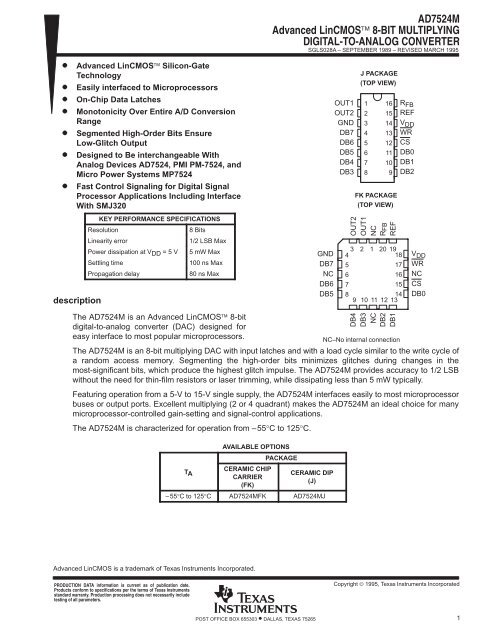
The <strong>AD7524</strong>M is an Advanced LinCMOS 8-<strong>bit</strong><br />
digital-to-analog converter (<strong>DAC</strong>) designed for<br />
easy interface to most popular microprocessors.<br />
POST OFFICE BOX 655303 • DALLAS, TEXAS 75265<br />
<strong>AD7524</strong>M<br />
Advanced LinCMOS 8-BIT MULTIPLYING<br />
DIGITAL-TO-ANALOG CONVERTER<br />
SGLS028A – SEPTEMBER 1989 – REVISED MARCH 1995<br />
The <strong>AD7524</strong>M is an 8-<strong>bit</strong> <strong>multiplying</strong> <strong>DAC</strong> with input latches and with a load cycle similar to the write cycle of<br />
a random access memory. Segmenting the high-order <strong>bit</strong>s minimizes glitches during changes in the<br />
most-significant <strong>bit</strong>s, which produce the highest glitch impulse. The <strong>AD7524</strong>M provides accuracy to 1/2 LSB<br />
without the need for thin-film resistors or laser trimming, while dissipating less than 5 mW typically.<br />
Featuring operation from a 5-V to 15-V single supply, the <strong>AD7524</strong>M interfaces easily to most microprocessor<br />
buses or output ports. Excellent <strong>multiplying</strong> (2 or 4 quadrant) makes the <strong>AD7524</strong>M an ideal choice for many<br />
microprocessor-controlled gain-setting and signal-control applications.<br />
The <strong>AD7524</strong>M is characterized for operation from –55°C to 125°C.<br />
TA<br />
AVAILABLE OPTIONS<br />
CERAMIC CHIP<br />
CARRIER<br />
(FK)<br />
PACKAGE<br />
CERAMIC DIP<br />
(J)<br />
–55°C to 125°C <strong>AD7524</strong>MFK <strong>AD7524</strong>MJ<br />
Advanced LinCMOS is a trademark of Texas Instruments Incorporated.<br />
PRODUCTION DATA information is current as of publication date.<br />
Products conform to specifications per the terms of Texas Instruments<br />
standard warranty. Production processing does not necessarily include<br />
testing of all parameters.<br />
GND<br />
DB7<br />
NC<br />
DB6<br />
DB5<br />
OUT1<br />
OUT2<br />
GND<br />
DB7<br />
DB6<br />
DB5<br />
DB4<br />
DB3<br />
J PACKAGE<br />
(TOP VIEW)<br />
1<br />
2<br />
3<br />
4<br />
5<br />
6<br />
7<br />
8<br />
16<br />
15<br />
14<br />
13<br />
12<br />
11<br />
10<br />
9<br />
FK PACKAGE<br />
(TOP VIEW)<br />
OUT2<br />
OUT1<br />
NC<br />
RFB<br />
REF<br />
3<br />
4<br />
2 1 20 19<br />
18<br />
5<br />
17<br />
6<br />
16<br />
7<br />
15<br />
8<br />
14<br />
9 10 11 12 13<br />
DB4<br />
DB3<br />
NC<br />
DB2<br />
DB1<br />
NC–No internal connection<br />
R FB<br />
REF<br />
V DD<br />
WR<br />
CS<br />
DB0<br />
DB1<br />
DB2<br />
V DD<br />
WR<br />
NC<br />
CS<br />
DB0<br />
Copyright © 1995, Texas Instruments Incorporated<br />
1
<strong>AD7524</strong>M<br />
Advanced LinCMOS 8-BIT MULTIPLYING<br />
DIGITAL-TO-ANALOG CONVERTER<br />
SGLS028A – SEPTEMBER 1989 – REVISED MARCH 1995<br />
functional block diagram<br />
REF 15<br />
CS<br />
WR<br />
operating sequence<br />
CS<br />
WR<br />
DB0 –DB7<br />
12<br />
13<br />
4<br />
DB7<br />
(MSB)<br />
10%<br />
Data Latches<br />
Data Inputs<br />
2 POST OFFICE BOX 655303 • DALLAS, TEXAS 75265<br />
2R<br />
S-1<br />
R<br />
S-2<br />
5<br />
R<br />
2R 2R 2R 2R<br />
S-3<br />
6<br />
R<br />
S-8<br />
11<br />
DB6 DB5 DB0<br />
(LSB)<br />
tsu(CS)<br />
ÎÎÎÎ<br />
tw(WR)<br />
ÎÎÎ<br />
ÎÎÎ<br />
10% 10%<br />
tsu(D)<br />
ÎÎÎÎ<br />
ÎÎÎÎ<br />
R<br />
16<br />
1<br />
2<br />
3<br />
RFB<br />
OUT1<br />
OUT2<br />
GND<br />
th(CS)<br />
ÎÎÎ<br />
ÎÎÎ<br />
th(D)<br />
ÎÎÎ<br />
ÎÎÎ
POST OFFICE BOX 655303 • DALLAS, TEXAS 75265<br />
<strong>AD7524</strong>M<br />
Advanced LinCMOS 8-BIT MULTIPLYING<br />
DIGITAL-TO-ANALOG CONVERTER<br />
SGLS028A – SEPTEMBER 1989 – REVISED MARCH 1995<br />
absolute maximum ratings over operating free-air temperature range (unless otherwise noted) †<br />
Supply voltage range, VDD . . . . . . . . . . . . . . . . . . . . . . . . . . . . . . . . . . . . . . . . . . . . . . . . . . . . . . . . . –0.3 V to 17 V<br />
Voltage between RFB and GND . . . . . . . . . . . . . . . . . . . . . . . . . . . . . . . . . . . . . . . . . . . . . . . . . . . . . . . . . . . . . ±25 V<br />
Digital input voltage range, VI . . . . . . . . . . . . . . . . . . . . . . . . . . . . . . . . . . . . . . . . . . . . . . . . . –0.3 V to VDD+0.3 V<br />
Reference voltage range, Vref . . . . . . . . . . . . . . . . . . . . . . . . . . . . . . . . . . . . . . . . . . . . . . . . . . . . . . . . . . . . . . ±25 V<br />
Peak digital input current, II . . . . . . . . . . . . . . . . . . . . . . . . . . . . . . . . . . . . . . . . . . . . . . . . . . . . . . . . . . . . . . . . 10 μA<br />
Operating free-air temperature range, TA . . . . . . . . . . . . . . . . . . . . . . . . . . . . . . . . . . . . . . . . . . . –55°C to 125°C<br />
Storage temperature range, Tstg . . . . . . . . . . . . . . . . . . . . . . . . . . . . . . . . . . . . . . . . . . . . . . . . . . . –65°C to 150°C<br />
Case temperature for 60 seconds, TC: FK package . . . . . . . . . . . . . . . . . . . . . . . . . . . . . . . . . . . . . . . . . . 260°C<br />
Lead temperature 1,6 mm (1/16 inch) from case for 60 seconds: J package . . . . . . . . . . . . . . . . . . . . . 300°C<br />
† Stresses beyond those listed under “absolute maximum ratings” may cause permanent damage to the device. These are stress ratings only, and<br />
functional operation of the device at these or any other conditions beyond those indicated under “recommended operating conditions” is not<br />
implied. Exposure to absolute-maximum-rated conditions for extended periods may affect device reliability.<br />
recommended operating conditions<br />
VDD = 5 V VDD = 15 V<br />
MIN NOM MAX MIN NOM MAX<br />
Supply voltage, VDD 4.75 5 5.25 14.5 15 15.5 V<br />
Reference voltage, Vref ±10 ±10 V<br />
High-level input voltage, VIH 2.4 13.5 V<br />
Low-level input volage, VIL 0.8 1.5 V<br />
CS setup time, tsu(CS) 40 40 ns<br />
CS hold time, th(CS) 0 0 ns<br />
Data bus input setup time, tsu(D) 25 25 ns<br />
Data bus input hold time, th(D) 10 10 ns<br />
Pulse duration, WR low, tw(WR) 40 40 ns<br />
Operating free-air temperature, TA –55 125 –55 125 °C<br />
UNIT<br />
3
<strong>AD7524</strong>M<br />
Advanced LinCMOS 8-BIT MULTIPLYING<br />
DIGITAL-TO-ANALOG CONVERTER<br />
SGLS028A – SEPTEMBER 1989 – REVISED MARCH 1995<br />
electrical characteristics over recommended operating free-air temperature range, V ref = 10 V,<br />
OUT1 and OUT2 at GND (unless otherwise noted)<br />
PARAMETER TEST CONDITIONS<br />
IIH IIH High High-level level input current VI VI =VDD = VDD<br />
IIL IIL Low Low-level level input current VI VI =0 = 0<br />
IIpkg k<br />
IDD<br />
kSVS kSVS<br />
Ci<br />
OUT1<br />
DB0–DB7 at 0,<br />
WR and CS at 0 V<br />
4 POST OFFICE BOX 655303 • DALLAS, TEXAS 75265<br />
VDD = 5 V VDD = 15 V<br />
MIN TYP MAX MIN TYP MAX<br />
Full-range 10 10<br />
25°C 1 1<br />
Full-range –10 –10<br />
25°C –1 –1<br />
Full-range ±400 ±200<br />
Output leakage g<br />
Vref = ±10 V 25°C ±50 ±50<br />
current<br />
OUT2<br />
DB0–DB7 at VDD,<br />
WR and CS at 0<br />
Full-range ±400 ±200<br />
Vref = ±10 V 25°C ±50 ±50<br />
Supply current<br />
Supply y voltage g sensitivity, y,<br />
Δgain/ΔVDD<br />
Input capacitance, DB0–DB7,<br />
WR, CS<br />
Quiescent DB0–DB7 at VIHmin or VILmax 2 2 mA<br />
Standby DB0 DB0–DB7 DB7at0VorVDD<br />
at 0 V or VDD<br />
OUT1<br />
Output<br />
OUT2<br />
CCo<br />
capacitance OUT1<br />
OUT2<br />
Reference input impedance<br />
(REF to GND)<br />
ΔVDD ΔVDD = 10%<br />
Full-range 500 500<br />
25°C 100 100<br />
UNIT<br />
μA<br />
μA<br />
nA<br />
μA<br />
Full-range 0.16 0.04 %/%<br />
25°C 0.002 0.02 0.001 0.02 pF<br />
VI = 0 5 5 pF<br />
DB0 DB0–DB7 DB7 at 0, 0 WR and CS at at0V 0 V<br />
DB0 DB0–DB7 DB7 at VDD, V WR and and CS at at0V 0 V<br />
30 30<br />
120 120<br />
120 120<br />
30 30<br />
pF<br />
5 20 5 20 kΩ<br />
operating characteristics over recommended operating free-air temperature range, V ref = 10 V,<br />
OUT1 and OUT2 at GND (unless otherwise noted)<br />
PARAMETER TEST CONDITIONS<br />
VCC = 5 V VDD = 15 V<br />
MIN MAX MIN MAX<br />
Linearity error ±0.2 ±0.2 %FSR<br />
Gain error See Note 1<br />
UNIT<br />
Full range ±1.4 ±0.6<br />
%FSR<br />
25°C ±1 ±0.5 %FSR<br />
Settling time (to 1/2 LSB) See Note 2 100 100 ns<br />
Propagation delay from digital input to<br />
90% of final analog output current<br />
See Note 2 80 80 ns<br />
Vref = ±10 V (100 kHz sinewave), Full range 0.5 0.5<br />
Feedthrough at OUT1 or OUT2 ref ( ),<br />
%FSR<br />
WR and CS at 0, DB0–DB7 at 0 25°C 0.25 0.25 %FSR<br />
Temperature coefficient of gain TA = 25°C to tmin or tmax ± 0.004 ±0.001 %FSR/<br />
°C<br />
NOTES: 1. Gain error is measured using the internal feedback resistor. Nominal Full Scale Range (FSR) = Vref – 1 LSB.<br />
2. OUT1 load = 100 Ω, Cext = 13 pF, WR at 0 V, CS at 0 V, DB0–DB7 at 0 V to VDD or VDD to 0 V.
PRINCIPLES OF OPERATION<br />
POST OFFICE BOX 655303 • DALLAS, TEXAS 75265<br />
<strong>AD7524</strong>M<br />
Advanced LinCMOS 8-BIT MULTIPLYING<br />
DIGITAL-TO-ANALOG CONVERTER<br />
SGLS028A – SEPTEMBER 1989 – REVISED MARCH 1995<br />
The <strong>AD7524</strong>M is an 8-<strong>bit</strong> <strong>multiplying</strong> D/A converter consisting of an inverted R-2R ladder, analog switches, and<br />
data input latches. Binary weighted currents are switched between the OUT1 and OUT2 bus lines, thus<br />
maintaining a constant current in each ladder leg independent of the switch state. The high-order <strong>bit</strong>s are<br />
decoded and these decoded <strong>bit</strong>s, through a modification in the R-2R ladder, control three equally weighted<br />
current sources. Most applications only require the addition of an external operational amplifier and a voltage<br />
reference.<br />
The equivalent circuit for all digital inputs low is seen in Figure 1. With all digital inputs low, the entire reference<br />
current, Iref, is switched to OUT2. The current source 1/256 represents the constant current flowing through the<br />
termination resistor of the R-2R ladder, while the current source IIkg represents leakage currents to the<br />
substrate. The capacitances appearing at OUT1 and OUT2 are dependent upon the digital input code. With all<br />
digital inputs high, the off-state switch capacitance (30 pF maximum) appears at OUT2 and the on-state switch<br />
capacitance (120 pF maximum) appears at OUT1. With all digital inputs low, the situation is reversed as shown<br />
in Figure 1. Analysis of the circuit for all digital inputs high is similar to Figure 1; however, in this case, Iref would<br />
be switched to OUT1.<br />
Interfacing the <strong>AD7524</strong>M D/A converter to a microprocessor is accomplished via the data bus and the CS and<br />
WR control signals. When CS and WR are both low, the <strong>AD7524</strong>M analog output responds to the data activity<br />
on the DB0–DB7 data bus inputs. In this mode, the input latches are transparent and input data directly affects<br />
the analog output. When either the CS signal or WR signal goes high, the data on the DB0–DB7 inputs are<br />
latched until the CS and WR signals go low again. When CS is high, the data inputs are disabled regardless<br />
of the state of the WR signal.<br />
The <strong>AD7524</strong>M is capable of performing 2-quadrant or full 4-quadrant multiplication. Circuit configurations for<br />
2-quadrant or 4-quadrant multiplication are shown in Figures 2 and 3. Input coding for unipolar and bipolar<br />
operation are summarized in Tables 1 and 2, respectively.<br />
5
<strong>AD7524</strong>M<br />
Advanced LinCMOS 8-BIT MULTIPLYING<br />
DIGITAL-TO-ANALOG CONVERTER<br />
SGLS028A – SEPTEMBER 1989 – REVISED MARCH 1995<br />
DB0 –DB7<br />
CS<br />
WR<br />
PRINCIPLES OF OPERATION<br />
REF OUT2<br />
RA = 2 kΩ<br />
(see Note A)<br />
1/256<br />
6 POST OFFICE BOX 655303 • DALLAS, TEXAS 75265<br />
I1kg<br />
I1kg<br />
R<br />
30 pF<br />
120 pF<br />
RFB<br />
OUT1<br />
Figure 1. <strong>AD7524</strong>M Equivalent Circuit With All Digital Inputs Low<br />
DB0 –DB7<br />
Vref<br />
CS<br />
WR<br />
RA = 2 kΩ<br />
(see Note A)<br />
Vref<br />
VDD<br />
RFB<br />
GND<br />
OUT1<br />
OUT2<br />
RB<br />
C (see Note B)<br />
Figure 2. Unipolar Operation (2-Quadrant Multiplication)<br />
VDD<br />
GND<br />
RFB<br />
OUT1<br />
OUT2<br />
RB<br />
C (see Note B)<br />
–<br />
+<br />
–<br />
+<br />
20 kΩ<br />
10 kΩ<br />
Figure 3. Bipolar Operation (4-Quadrant Operation)<br />
20 kΩ<br />
–<br />
+<br />
5 kΩ<br />
Output<br />
NOTES: A. RA and RB used only if gain adjustment is required.<br />
B. C phase compensation (10 – 15 pF) is required when using high-speed amplifiers to prevent ringing or oscillation.<br />
Output
microprocessor interfaces<br />
Z-80A<br />
D0–D7<br />
WR<br />
IORQ<br />
A0–A15<br />
PRINCIPLES OF OPERATION<br />
Table 1. Unipolar Binary Code<br />
DIGITAL INPUT<br />
(see NOTE 3) ANALOG OUTPUT<br />
MSB LSB<br />
11111111<br />
10000001<br />
10000000<br />
01111111<br />
00000001<br />
00000000<br />
NOTES: 3. LSB = 1/256 (Vref).<br />
POST OFFICE BOX 655303 • DALLAS, TEXAS 75265<br />
<strong>AD7524</strong>M<br />
Advanced LinCMOS 8-BIT MULTIPLYING<br />
DIGITAL-TO-ANALOG CONVERTER<br />
SGLS028A – SEPTEMBER 1989 – REVISED MARCH 1995<br />
–Vref (255/256)<br />
–Vref (129/256)<br />
–Vref (128/256) = –Vref /2<br />
–Vref (127/256)<br />
–Vref (1/256)<br />
0<br />
Table 2. Bipolar (Offset Binary) Code<br />
DIGITAL INPUT<br />
(see NOTE 4) ANALOG OUTPUT<br />
MSB LSB<br />
11111111<br />
10000001<br />
10000000<br />
01111111<br />
00000001<br />
00000000<br />
NOTES: 4. LSB = 1/128 (Vref).<br />
Decode<br />
Logic<br />
Vref (127/128)<br />
Vref (128)<br />
0<br />
–Vref (128)<br />
–Vref (127/128)<br />
–Vref<br />
Data Bus<br />
Address Bus<br />
WR<br />
DB0 –DB7<br />
Figure 4. <strong>AD7524</strong>M–Z-80A Interface<br />
<strong>AD7524</strong>M<br />
CS<br />
OUT1<br />
OUT2<br />
7
<strong>AD7524</strong>M<br />
Advanced LinCMOS 8-BIT MULTIPLYING<br />
DIGITAL-TO-ANALOG CONVERTER<br />
SGLS028A – SEPTEMBER 1989 – REVISED MARCH 1995<br />
8051<br />
6800<br />
Φ2<br />
VMA<br />
A0–A15<br />
A8–A15<br />
D0–D7<br />
ALE<br />
WR<br />
AD0 –AD7<br />
PRINCIPLES OF OPERATION<br />
Decode<br />
Logic<br />
Data Bus<br />
Address Bus<br />
Figure 5. <strong>AD7524</strong>M–6800 Interface<br />
Address Bus<br />
8-Bit<br />
Latch<br />
Decode<br />
Logic<br />
Address/Data Bus<br />
Figure 6. <strong>AD7524</strong>M–8051 Interface<br />
8 POST OFFICE BOX 655303 • DALLAS, TEXAS 75265<br />
DB0 –DB7<br />
WR <strong>AD7524</strong>M<br />
CS<br />
WR<br />
CS<br />
OUT1<br />
OUT2<br />
<strong>AD7524</strong>M<br />
DB0 –DB7<br />
OUT1<br />
OUT2
IMPORTANT NOTICE<br />
Texas Instruments and its subsidiaries (TI) reserve the right to make changes to their products or to discontinue<br />
any product or service without notice, and advise customers to obtain the latest version of relevant information<br />
to verify, before placing orders, that information being relied on is current and complete. All products are sold<br />
subject to the terms and conditions of sale supplied at the time of order acknowledgement, including those<br />
pertaining to warranty, patent infringement, and limitation of liability.<br />
TI warrants performance of its semiconductor products to the specifications applicable at the time of sale in<br />
accordance with TI’s standard warranty. Testing and other quality control techniques are utilized to the extent<br />
TI deems necessary to support this warranty. Specific testing of all parameters of each device is not necessarily<br />
performed, except those mandated by government requirements.<br />
CERTAIN APPLICATIONS USING SEMICONDUCTOR PRODUCTS MAY INVOLVE POTENTIAL RISKS OF<br />
DEATH, PERSONAL INJURY, OR SEVERE PROPERTY OR ENVIRONMENTAL DAMAGE (“CRITICAL<br />
APPLICATIONS”). TI SEMICONDUCTOR PRODUCTS ARE NOT DESIGNED, AUTHORIZED, OR<br />
WARRANTED TO BE SUITABLE FOR USE IN LIFE-SUPPORT DEVICES OR SYSTEMS OR OTHER<br />
CRITICAL APPLICATIONS. INCLUSION OF TI PRODUCTS IN SUCH APPLICATIONS IS UNDERSTOOD TO<br />
BE FULLY AT THE CUSTOMER’S RISK.<br />
In order to minimize risks associated with the customer’s applications, adequate design and operating<br />
safeguards must be provided by the customer to minimize inherent or procedural hazards.<br />
TI assumes no liability for applications assistance or customer product design. TI does not warrant or represent<br />
that any license, either express or implied, is granted under any patent right, copyright, mask work right, or other<br />
intellectual property right of TI covering or relating to any combination, machine, or process in which such<br />
semiconductor products or services might be or are used. TI’s publication of information regarding any third<br />
party’s products or services does not constitute TI’s approval, warranty or endorsement thereof.<br />
Copyright © 1998, Texas Instruments Incorporated
This datasheet has been download from:<br />
www.datasheetcatalog.com<br />
Datasheets for electronics components.