DM93S41 ALU.pdf
DM93S41 ALU.pdf
DM93S41 ALU.pdf

Create successful ePaper yourself
Turn your PDF publications into a flip-book with our unique Google optimized e-Paper software.
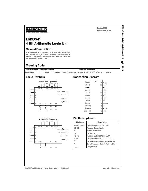
<strong>DM93S41</strong><br />
4-Bit Arithmetic Logic Unit<br />
General Description<br />
The <strong>DM93S41</strong> 4-bit arithmetic logic units can perform all<br />
the possible 16 logic operations on two variables and a<br />
variety of arithmetic operations; the Add and Subtract<br />
modes are the most important.<br />
Ordering Code:<br />
Order Number Package Number Package Description<br />
October 1988<br />
Revised May 2000<br />
<strong>DM93S41</strong>N N24A 24-Lead Plastic Dual-In-Line Package (PDIP), JEDEC MS-010, 0.600 Wide<br />
Logic Symbols<br />
Active LOW Operands<br />
Active HIGH Operands<br />
Connection Diagram<br />
Pin Descriptions<br />
Pin Name Description<br />
A0–A3, B0–B3 Operand Inputs (Active LOW)<br />
S0–S3 Function Select Inputs<br />
M Mode Control Input<br />
Cn Carry Input<br />
F0–F3 Function Outputs (Active LOW)<br />
A = B Comparator Output<br />
G Carry Generate Output (Active LOW)<br />
P Carry Propagate Output (Active LOW)<br />
© 2000 Fairchild Semiconductor Corporation DS009805 www.fairchildsemi.com<br />
C n+4<br />
Carry Output<br />
<strong>DM93S41</strong> 4-Bit Arithmetic Logic Unit
<strong>DM93S41</strong><br />
Functional Description<br />
The <strong>DM93S41</strong> is a 4-bit high speed parallel arithmetic logic<br />
unit (<strong>ALU</strong>). Controlled by the four Function Select inputs<br />
(S0–S3) and the Mode Control input (M), it can perform all<br />
the 16 possible operations or 16 different arithmetic operations<br />
on active HIGH or active LOW operands. The Function<br />
Table below lists these operations.<br />
When the Mode Control input (M) is HIGH, all internal carries<br />
are inhibited and the device performs logic operations<br />
on the individual bits as listed. When the Mode Control<br />
input is LOW, the carries are enabled and the device performs<br />
arithmetic operations on the two 4-bit words. The<br />
device incorporates full internal carry lookahead and provides<br />
for either ripple carry between devices using the C n+4<br />
output, or for carry lookahead between packages using the<br />
signals P (Carry Propagate) and G (Carry Generate). P<br />
and G are not affected by carry in. When speed requirements<br />
are not stringent, the <strong>DM93S41</strong> can be used in a<br />
simple ripple carry mode by connecting the Carry output<br />
(C n+4 ) signal to the Carry input (C n ) of the next unit. For<br />
super high speed operation the Schottky <strong>DM93S41</strong> should<br />
be used in conjunction with the '42 carry lookahead circuit.<br />
Function Table<br />
H = HIGH Voltage Level<br />
L = LOW Voltage Level<br />
Note 1: Each bit is shifted to the next more significant position<br />
Note 2: Arithmetic operations expressed in 2s complement notation<br />
www.fairchildsemi.com 2<br />
The A = B output from the <strong>DM93S41</strong> goes HIGH when all<br />
four F n outputs are HIGH and can be used to indicate logic<br />
equivalence over four bits when the unit is in the subtract<br />
mode. The A = B output is open-collector and can be wired-<br />
AND with the other A = B outputs to give a comparison for<br />
more than four bits. The A = B signal can also be used with<br />
the C n+4 signal to indicate A > B and A < B.<br />
The Function Table lists the arithmetic operations that are<br />
performed without a carry in. An incoming carry adds a one<br />
to each operation. Thus select code LHHL generates A<br />
minus B minus 1 (2s complement notation) without a carry<br />
in and generates A minus B when a carry is applied.<br />
Because subtraction is actually performed by complementary<br />
addition (1s complement), a carry out means borrow;<br />
thus a carry is generated when there is no underflow and<br />
no carry is generated when there is underflow.<br />
As indicated the '41 can be used with either active LOW<br />
inputs producing active LOW outputs or with active HIGH<br />
inputs producing active HIGH outputs. For either case the<br />
table lists the operations that are performed to the operands<br />
labeled inside the logic symbol.<br />
Mode Select Active LOW Inputs Active HIGH Inputs<br />
Inputs & Outputs & Outputs<br />
Logic Arithmetic (Note 2) Logic Arithmetic (Note 2)<br />
S3 S2 S1 S0 (M = H) (M = L) (C n = L) (M = H) (M = L) (C n = H)<br />
L L L L A A minus 1 A A<br />
L L L H AB AB minus 1 A + B A + B<br />
L L H L A + B AB minus 1 AB A + B<br />
L L H H Logic 1 minus 1 Logic 0 minus 1<br />
L H L L A + B A plus (A + B) AB A plus AB<br />
L H L H B AB plus (A + B) B (A +B) plus AB<br />
L H H L A ⊕ B A minus B minus 1 A ⊕ B A minus B minus 1<br />
L H H H A + B A + B AB AB minus 1<br />
H L L L AB A plus (A + B) A + B A plus AB<br />
H L L H A ⊕ B A plus B A ⊕ B A plus B<br />
H L H L B AB plus (A + B) B (A + B) plus AB<br />
H L H H A + B A + B AB AB minus 1<br />
H H L L Logic 0 A plus A (Note 1) Logic 1 A plus A (Note 1)<br />
H H L H AB AB plus A A + B (A + B) plus A<br />
H H H L AB AB minus A A + B (A + B) plus A<br />
H H H H A A A A minus 1
Symbol<br />
TABLE 1. SUM MODE TEST Function Inputs: S0 = S3 = 4.5V, S1 = S2 = M = 0V<br />
Input Other Input Same Bit Other Data Input Output<br />
Under Apply Apply Apply Apply Under<br />
Test 4.5V GND 4.5V GND Test<br />
t PLH , t PHL A i B i None Remaining A to B C n F i<br />
t PLH , t PHL B i A i None Remaining A to B C n F i<br />
t PLH, t PHL A i B i None C n Remaining A and B F i + 1<br />
t PLH , t PHL B i A i None C n Remaining A and B F i + 1<br />
t PLH , t PHL A B None None Remaining A and B, C n P<br />
t PLH, t PHL B A None None Remaining A and B, C n P<br />
t PLH , t PHL A None B Remaining B Remaining A, C n G<br />
t PLH, t PHL B None A Remaining B Remaining A, C n G<br />
t PLH, t PHL A None B Remaining B Remaining A, C n C n + 4<br />
t PLH , t PHL B None A Remaining B Remaining A, C n C n + 4<br />
t PLH, t PHL C n None None All A All B Any F or C n + 4<br />
Symbol<br />
TABLE 2. DIFF MODE TEST Function Inputs: S1 = S2 = 4.5V,S0 = S3 = M = 0V<br />
Input Other Input Same Bit Other Data Inputs Output<br />
Under Apply Apply Apply Apply Under<br />
Test 4.5V GND 4.5V GND Test<br />
t PLH, t PHL A None B Remaining A Remaining B, C n F i<br />
t PLH , t PHL B A None Remaining A Remaining B, C n F i<br />
t PLH, t PHL A i None B i Remaining B, C n Remaining A F i + 1<br />
t PLH, t PHL B i A i None Remaining B, C n Remaining A F i + 1<br />
t PLH , t PHL A None B None Remaining A and B, C n P<br />
t PLH, t PHL B A None None Remaining A and B, C n P<br />
t PLH, t PHL A B None None Remaining A and B, C n G<br />
t PLH , t PHL B None A None Remaining A and B, C n G<br />
t PLH, t PHL A None B Remaining A Remaining B, C n A = B<br />
t PLH, t PHL B A None Remaining A Remaining B, C n A = B<br />
t PLH , t PHL A B None None Remaining A and B, C n C n + 4<br />
t PLH, t PHL B None A None Remaining A and B, C n C n + 4<br />
t PLH , t PHL C n None None All A and B None C n + 4<br />
Symbol<br />
TABLE 3. LOGIC MODE TEST Function Inputs: S1 = S2 = M = 4.5V, S0 = S3 = 0V<br />
Input Other Input Same Bit Other Data Inputs Output<br />
Under Apply Apply Apply Apply Under<br />
Test 4.5V GND 4.5V GND Test<br />
t PLH , t PHL A B None None Remaining A and B, C n Any F<br />
t PLH, t PHL B A None None Remaining A and B, C n Any F<br />
3 www.fairchildsemi.com<br />
<strong>DM93S41</strong>
<strong>DM93S41</strong><br />
Logic Diagram<br />
www.fairchildsemi.com 4
Absolute Maximum Ratings(Note 3)<br />
Supply Voltage 7V<br />
Input Voltage: 5.5V<br />
Operating Free Air Temperature Range 0°C to +70°C<br />
Storage Temperature Range −65°C to +150°C<br />
Recommended Operating Conditions<br />
Electrical Characteristics<br />
over recommended operating free air temperature range (unless otherwise noted)<br />
Note 4: All typicals are at V CC = 5V, T A = 25°C.<br />
Note 5: Not more than one output should be shorted at a time, and the duration should not exceed one second.<br />
Note 3: The “Absolute Maximum Ratings” are those values beyond which<br />
the safety of the device cannot be guaranteed. The device should not be<br />
operated at these limits. The parametric values defined in the Electrical<br />
Characteristics tables are not guaranteed at the absolute maximum ratings.<br />
The “Recommended Operating Conditions” table will define the conditions<br />
for actual device operation.<br />
Symbol Parameter Min Nom Max Units<br />
V CC Supply Voltage 4.75 5 5.25 V<br />
V IH HIGH Level Input Voltage 2 V<br />
V IL LOW Level Input Voltage 0.8 V<br />
I OH HIGH Level Output Current −1 mA<br />
I OL LOW Level Output Current 20 mA<br />
T A Free Air Operating Temperature 0 70 °C<br />
Symbol Parameter Conditions Min<br />
Typ<br />
(Note 4)<br />
Max Units<br />
V I Input Clamp Voltage V CC = Min, I I = − 18 mA −1.2 V<br />
V OH HIGH Level V CC = Min, I OH = Max<br />
Output Voltage V IL = Max<br />
V OL LOW Level V CC = Min, I OL = Max<br />
Output Voltage V IH = Min<br />
2.7 3.4 V<br />
0.35 0.5 V<br />
I I Input Current @ Max Input Voltage V CC = Max, V I = 5.5V 1 mA<br />
I IH HIGH Level Input Current V CC = Max, V I = 2.7V 50 µA<br />
I IL LOW Level Input Current V CC = Max, V I = 0.5V −1.6 mA<br />
I OS Short Circuit Output Current V CC = Max (Note 5) −40 −100 mA<br />
I CCL Supply Current V CC = Max<br />
M, S0–S3 = 4.5V 150 mA<br />
All Other Inputs = 0V<br />
I CCH Supply Current V CC = Max<br />
C n , B0–B3 = GND 140 mA<br />
All Other Inputs = 4.5V<br />
5 www.fairchildsemi.com<br />
<strong>DM93S41</strong>
<strong>DM93S41</strong><br />
Switching Characteristics<br />
V CC = +5.0V, T A = +25°C<br />
www.fairchildsemi.com 6<br />
CL = 15 pF<br />
Symbol Parameter Conditions R L = 280Ω Units<br />
Min Max<br />
t PLH Propagation Delay M = GND 12<br />
t PHL C n to C n + 4 12<br />
t PLH Propagation Delay M = GND 12<br />
t PHL C n to F 12<br />
t PLH Propagation Delay M, S1, S2 = GND 14<br />
t PHL A n or B n to G S0, S3 = 4.5V 14<br />
t PLH Propagation Delay M, S0, S3 = GND 15<br />
t PHL A n or B n to G S1, S2 = 4.5V 15<br />
t PLH Propagation Delay M, S1, S2 = GND 14<br />
t PHL A n or B n to P S0, S3 = 4.5V 14<br />
t PLH Propagation Delay M, S0, S3 = GND 15<br />
t PHL A n or B n to P S1, S2 = 4.5V 15<br />
t PLH Propagation Delay M, S1, S3 = GND 20<br />
t PHL A i or B i to F i S0, S3 = 4.5V 20<br />
t PLH Propagation Delay M, S0, S3 = GND 21<br />
t PHL A i or B i to F i S1, S2 = 4.5V 21<br />
t PLH Propagation Delay M, S1, S2 = GND 24<br />
t PHL A i or B i to F i + 1 S0, S3 = 4.5V 24<br />
t PLH Propagation Delay M, S0, S3 = GND 25<br />
t PHL A i or B i to F i + 1 S1, S2 = 4.5V 25<br />
t PLH Propagation Delay M = 4.5V 20<br />
t PHL A n or B n to F 20<br />
t PLH Propagation Delay M, S1, S2 = GND 18.5<br />
t PHL A n or B n to C n + 1 S0, S3 = 4.5V 18.5<br />
t PLH Propagation Delay M, S0, S3 = GND 23<br />
t PHL A n or B n to C n + 1 S1, S2 = 4.5V 23<br />
t PLH Propagation Delay M, S0, S3 = GND 23<br />
t PHL A n or B n to A = B S1, S2 = 4.5V 23<br />
R L = 400Ω to 5.0V<br />
ns<br />
ns<br />
ns<br />
ns<br />
ns<br />
ns<br />
ns<br />
ns<br />
ns<br />
ns<br />
ns<br />
ns<br />
ns<br />
ns
Physical Dimensions inches (millimeters) unless otherwise noted<br />
24-Lead Plastic Dual-In-Line Package (PDIP), JEDEC MS-010, 0.600 Wide<br />
Package Number N24A<br />
Fairchild does not assume any responsibility for use of any circuitry described, no circuit patent licenses are implied and<br />
Fairchild reserves the right at any time without notice to change said circuitry and specifications.<br />
LIFE SUPPORT POLICY<br />
FAIRCHILD’S PRODUCTS ARE NOT AUTHORIZED FOR USE AS CRITICAL COMPONENTS IN LIFE SUPPORT<br />
DEVICES OR SYSTEMS WITHOUT THE EXPRESS WRITTEN APPROVAL OF THE PRESIDENT OF FAIRCHILD<br />
SEMICONDUCTOR CORPORATION. As used herein:<br />
1. Life support devices or systems are devices or systems<br />
which, (a) are intended for surgical implant into the<br />
body, or (b) support or sustain life, and (c) whose failure<br />
to perform when properly used in accordance with<br />
instructions for use provided in the labeling, can be reasonably<br />
expected to result in a significant injury to the<br />
user.<br />
2. A critical component in any component of a life support<br />
device or system whose failure to perform can be reasonably<br />
expected to cause the failure of the life support<br />
device or system, or to affect its safety or effectiveness.<br />
www.fairchildsemi.com<br />
7 www.fairchildsemi.com<br />
<strong>DM93S41</strong> 4-Bit Arithmetic Logic Unit