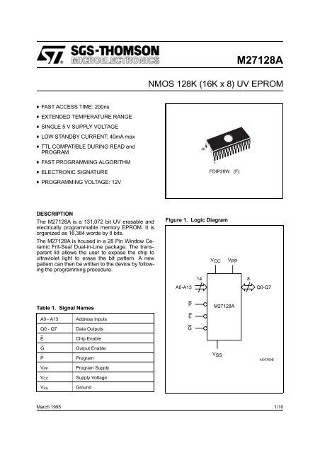
M27128A
M27128A
M27128A

You also want an ePaper? Increase the reach of your titles
YUMPU automatically turns print PDFs into web optimized ePapers that Google loves.
FAST ACCESS TIME: 200ns<br />
EXTENDED TEMPERATURE RANGE<br />
SINGLE 5 V SUPPLY VOLTAGE<br />
LOW STANDBY CURRENT: 40mA max<br />
TTL COMPATIBLE DURING READ and<br />
PROGRAM<br />
FAST PROGRAMMING ALGORITHM<br />
ELECTRONIC SIGNATURE<br />
PROGRAMMING VOLTAGE: 12V<br />
DESCRIPTION<br />
The <strong>M27128A</strong> is a 131,072 bit UV erasable and<br />
electrically programmable memory EPROM. It is<br />
organized as 16,384 words by 8 bits.<br />
The <strong>M27128A</strong> is housed in a 28 Pin Window Ceramic<br />
Frit-Seal Dual-in-Line package. The transparent<br />
lid allows the user to expose the chip to<br />
ultraviolet light to erase the bit pattern. A new<br />
pattern can then be written to the device by following<br />
the programming procedure.<br />
Table 1. Signal Names<br />
A0 - A13 Address Inputs<br />
Q0 - Q7 Data Outputs<br />
E Chip Enable<br />
G Output Enable<br />
P Program<br />
VPP<br />
VCC<br />
VSS<br />
Program Supply<br />
Supply Voltage<br />
Ground<br />
Figure 1. Logic Diagram<br />
A0-A13<br />
P<br />
E<br />
G<br />
14<br />
V CC<br />
V PP<br />
<strong>M27128A</strong><br />
VSS<br />
<strong>M27128A</strong><br />
NMOS 128K (16K x 8) UV EPROM<br />
28<br />
1<br />
FDIP28W (F)<br />
8<br />
Q0-Q7<br />
AI00769B<br />
March 1995 1/10
<strong>M27128A</strong><br />
Table 2. Absolute Maximum Ratings<br />
Symbol Parameter Value Unit<br />
TA Ambient Operating Temperature grade 1<br />
grade 6<br />
0 to 70<br />
–40 to 85<br />
°C<br />
TBIAS Temperature Under Bias grade 1<br />
grade 6<br />
–10 to 80<br />
–50 to 95<br />
°C<br />
TSTG Storage Temperature –65 to 125 °C<br />
VIO Input or Output Voltages –0.6 to 6.25 V<br />
VCC Supply Voltage –0.6 to 6.25 V<br />
VA9 A9 Voltage –0.6 to 13.5 V<br />
VPP Program Supply –0.6 to 14 V<br />
Note: Except for the rating "Operating Temperature Range", stresses above those listed in the Table "Absolute Maximum Ratings" may cause<br />
permanent damage to the device. These are stress ratings only and operation of the device at these or any other conditions above those<br />
indicated in the Operating sections of this specification is not implied. Exposure to Absolute Maximum Rating conditions for extended periods<br />
may affect device reliability. Refer also to the SGS-THOMSON SURE Program and other relevant quality documents.<br />
Figure 2. DIP Pin Connections<br />
VPP 1<br />
28 VCC A12 2<br />
27 P<br />
A7 3<br />
26 A13<br />
A6 4<br />
25 A8<br />
A5 5<br />
24 A9<br />
A4 6<br />
23 A11<br />
A3<br />
A2<br />
7<br />
8<br />
<strong>M27128A</strong><br />
22<br />
21<br />
G<br />
A10<br />
A1 9<br />
20 E<br />
A0 10<br />
19 Q7<br />
Q0 11<br />
18 Q6<br />
Q1 12<br />
17 Q5<br />
Q2 13<br />
16 Q4<br />
VSS 14<br />
15 Q3<br />
AI00770<br />
DEVICE OPERATION<br />
The seven modes of operation of the <strong>M27128A</strong> are<br />
listed in the Operating Modes table. A single 5V<br />
power supply is required in the read mode. All<br />
inputs are TTL levels except for VPP and 12V on A9<br />
for Electronic Signature.<br />
2/10<br />
Read Mode<br />
The <strong>M27128A</strong> has two control functions, both of<br />
which must be logically satisfied in order to obtain<br />
data at the outputs. Chip Enable (E) is the power<br />
control and should be used for device selection.<br />
Output Enable (G) is the output control and should<br />
be used to gate data to the output pins, independent<br />
of device selection.<br />
Assuming that the addresses are stable, address<br />
access time (tAVQV) is equal to the delay from E to<br />
output (tELQV). Data is available at the outputs after<br />
the falling edge of G, assuming that E has been low<br />
and the addresses have been stable for at least<br />
tAVQV-tGLQV.<br />
Standby Mode<br />
The <strong>M27128A</strong> has a standby mode which reduces<br />
the maximum active power current from 85mA to<br />
40mA. The <strong>M27128A</strong> is placed in the standby mode<br />
by applying a TTL high signal to the E input. When<br />
in the standby mode, the outputs are in a high<br />
impedance state, independent of the G input.<br />
Two Line Output Control<br />
Because EPROMs are usually used in larger memory<br />
arrays, this product features a 2 line control<br />
function which accommodates the use of multiple<br />
memory connection. The two line control function<br />
allows:<br />
a. the lowest possible memory power dissipation,<br />
b. complete assurance that output bus contention<br />
will not occur.
DEVICE OPERATION (cont’d)<br />
For the most efficient use of these two control lines,<br />
E should be decoded and used as the primary<br />
device selecting function, while G should be made<br />
a common connection to all devices in the array<br />
and connected to the READ line from the system<br />
control bus.<br />
This ensures that all deselected memory devices<br />
are in their low power standby mode and that the<br />
output pins are only active when data is required<br />
from a particular memory device.<br />
System Considerations<br />
The power switching characteristics of fast<br />
EPROMs require careful decoupling of the devices.<br />
The supply current, ICC, has three segments that<br />
are of interest to the system designer: the standby<br />
current level, the active current level, and transient<br />
current peaks that are produced by the falling and<br />
rising edges of E. The magnitude of this transient<br />
current peaks is dependent on the capacitive and<br />
inductive loading of the device at the output. The<br />
associated transient voltage peaks can be suppressed<br />
by complying with the two line output<br />
control and by properly selected decoupling capacitors.<br />
It is recommended that a 1μF ceramic<br />
capacitor be used on every device between VCC<br />
and VSS. This should be a high frequency capacitor<br />
Table 3. Operating Modes<br />
of low inherent inductance and should be placed<br />
as close to the device as possible. In addition, a<br />
4.7μF bulk electrolytic capacitor should be used<br />
between VCC and GND for every eight devices. The<br />
bulk capacitor should be located near the power<br />
supply connection point. The purpose of the bulk<br />
capacitor is to overcome the voltage drop caused<br />
by the inductive effects of PCB traces.<br />
Programming<br />
When delivered (and after each erasure for UV<br />
EPPROM), all bits of the <strong>M27128A</strong> are in the “1"<br />
state. Data is introduced by selectively programming<br />
”0s" into the desired bit locations. Although<br />
only “0s” will be programmed, both “1s” and “0s”<br />
can be present in the data word. The only way to<br />
change a “0" to a ”1" is by ultraviolet light erasure.<br />
The <strong>M27128A</strong> is in the programming mode when<br />
VPP input is at 12.5V and E and P are at TTL low.<br />
The data to be programmed is applied 8 bits in<br />
parallel, to the data output pins. The levels required<br />
for the address and data inputs are TTL.<br />
Fast Programming Algorithm<br />
Fast Programming Algorithm rapidly programs<br />
<strong>M27128A</strong> EPROMs using an efficient and reliable<br />
method suited to the production programming environment.<br />
Programming reliability is also ensured<br />
as the incremental program margin of each byte is<br />
Mode E G P A9 VPP Q0 - Q7<br />
Read VIL VIL VIH X VCC Data Out<br />
Output Disable VIL VIH VIH X VCC Hi-Z<br />
Program VIL VIH VIL Pulse X VPP Data In<br />
Verify VIL VIL VIH X VPP Data Out<br />
Program Inhibit VIH X X X VPP Hi-Z<br />
Standby VIH X X X VCC Hi-Z<br />
Electronic Signature<br />
Note: X = VIH or VIL, VID = 12V ± 0.5%.<br />
VIL VIL VIH VID VCC Codes Out<br />
Table 4. Electronic Signature<br />
<strong>M27128A</strong><br />
Identifier A0 Q7 Q6 Q5 Q4 Q3 Q2 Q1 Q0 Hex Data<br />
Manufacturer’s Code VIL 0 0 1 0 0 0 0 0 20h<br />
Device Code VIH 1 0 0 0 1 0 0 1 89h<br />
3/10
<strong>M27128A</strong><br />
AC MEASUREMENT CONDITIONS<br />
Input Rise and Fall Times ≤ 20ns<br />
Input Pulse Voltages 0.45V to 2.4V<br />
Input and Output Timing Ref. Voltages 0.8V to 2.0V<br />
Note that Output Hi-Z is defined as the point where data<br />
is no longer driven.<br />
Figure 3. AC Testing Input Output Waveforms<br />
2.4V<br />
0.45V<br />
2.0V<br />
0.8V<br />
AI00827<br />
Table 5. Capacitance (1) (TA = 25 °C, f = 1 MHz )<br />
Figure 4. AC Testing Load Circuit<br />
DEVICE<br />
UNDER<br />
TEST<br />
1.3V<br />
C L includes JIG capacitance<br />
1N914<br />
3.3kΩ<br />
C L = 100pF<br />
OUT<br />
AI00828<br />
Symbol Parameter Test Condition Min Max Unit<br />
CIN Input Capacitance VIN = 0V = 6 pF<br />
COUT Output Capacitance VOUT = 0V = 12 pF<br />
Note: 1. Sampled only, not 100% tested.<br />
Figure 5. Read Mode AC Waveforms<br />
4/10<br />
A0-A13<br />
E<br />
G<br />
Q0-Q7<br />
tAVQV<br />
tELQV<br />
tGLQV<br />
VALID<br />
tAXQX<br />
DATA OUT<br />
tEHQZ<br />
tGHQZ<br />
Hi-Z<br />
AI00771
Table 6. Read Mode DC Characteristics (1)<br />
(TA = 0 to 70 °C or –40 to 85 °C; VCC = 5V ± 5% or 5V ± 10%; VPP = VCC)<br />
Symbol Parameter Test Condition Min Max Unit<br />
ILI Input Leakage Current 0 ≤ VIN ≤ VCC ±10 μA<br />
ILO Output Leakage Current VOUT = VCC ±10 μA<br />
ICC Supply Current E = VIL, G = VIL 75 mA<br />
ICC1 Supply Current (Standby) E = VIH 35 mA<br />
IPP Program Current VPP = VCC 5 mA<br />
VIL Input Low Voltage –0.1 0.8 V<br />
VIH Input High Voltage 2 VCC + 1 V<br />
VOL Output Low Voltage IOL = 2.1mA = 0.45 V<br />
VOH Output High Voltage IOH = –400μA 2.4 V<br />
Note: 1. VCC must be applied simultaneously with or before VPP and removed simultaneously or after VPP.<br />
Table 7. Read Mode AC Characteristics (1)<br />
(TA = 0 to 70 °C or –40 to 85 °C; VCC = 5V ± 5% or 5V ± 10%; VPP = VCC)<br />
Symbol Alt Parameter<br />
tAVQV tACC<br />
tELQV tCE<br />
tGLQV tOE<br />
tEHQZ (2)<br />
tGHQZ (2)<br />
tDF<br />
tDF<br />
tAXQX tOH<br />
Address Valid to<br />
Output Valid<br />
Chip Enable Low to<br />
Output Valid<br />
Output Enable Low<br />
to Output Valid<br />
Chip Enable High to<br />
Output Hi-Z<br />
Output Enable High<br />
to Output Hi-Z<br />
Address Transition to<br />
Output Transition<br />
Test<br />
Condition<br />
E = VIL,<br />
G = VIL<br />
<strong>M27128A</strong><br />
-2, -20 blank, -25 -3, -30 -4<br />
Min Max Min Max Min Max Min Max<br />
Unit<br />
200 250 300 450 ns<br />
G = VIL 200 250 300 450 ns<br />
E = VIL 75 100 120 150 ns<br />
G = VIL 0 55 0 60 0 105 0 130 ns<br />
E = VIL 0 55 0 60 0 105 0 130 ns<br />
E = VIL,<br />
G = VIL<br />
0 0 0 0 ns<br />
Notes: 1. VCC must be applied simultaneously with or before VPP and removed simultaneously or after VPP.<br />
2. Sampled only, not 100% tested.<br />
<strong>M27128A</strong><br />
5/10
<strong>M27128A</strong><br />
Table 8. Programming Mode DC Characteristics (1)<br />
(TA = 25 °C; VCC = 6V ± 0.25V; VPP = 12.5V ± 0.3V)<br />
Symbol Parameter Test Condition Min Max Unit<br />
ILI Input Leakage Current VIL ≤ VIN ≤ VIH ±10 μA<br />
ICC Supply Current 100 mA<br />
IPP Program Current E = VIL 50 mA<br />
VIL Input Low Voltage –0.1 0.8 V<br />
VIH Input High Voltage 2 VCC + 1 V<br />
VOL Output Low Voltage IOL = 2.1mA 0.45 V<br />
VOH Output High Voltage IOH = –400μA 2.4 V<br />
VID A9 Voltage 11.5 12.5 V<br />
Note: 1. VCC must be applied simultaneously with or before VPP and removed simultaneously or after VPP.<br />
Table 9. Programming Mode AC Characteristics (1)<br />
(TA = 25 °C; VCC = 6V ± 0.25V; VPP = 12.5V ± 0.3V)<br />
Symbol Alt Parameter Test Condition Min Max Unit<br />
tAVPL tAS Address Valid to Program Low 2 μs<br />
tQVPL tDS Input Valid to Program Low 2 μs<br />
tVPHPL tVPS VPP High to Program Low 2 μs<br />
tVCHPL tVCS VCC High to Program Low 2 μs<br />
tELPL tCES<br />
Chip Enable Low to Program<br />
Low<br />
2 μs<br />
tPLPH tPW Program Pulse Width (Initial) Note 2 0.95 1.05 ms<br />
tPLPH tOPW<br />
Program Pulse Width<br />
(Overprogram)<br />
Note 3 2.85 78.75 ms<br />
tPHQX<br />
tQXGL<br />
tGLQV<br />
tGHQZ (4)<br />
tGHAX<br />
tDH<br />
tOES<br />
tOE<br />
tDFP<br />
tAH<br />
Program High to Input<br />
Transition<br />
Input Transition to Output<br />
Enable Low<br />
Output Enable Low to<br />
Output Valid<br />
Output Enable High to<br />
Output Hi-Z<br />
Output Enable High to<br />
Address Transition<br />
2 μs<br />
2 μs<br />
150 ns<br />
0 130 ns<br />
0 ns<br />
Notes: 1. VCC must be applied simultaneously with or before VPP and removed simultaneously or after VPP.<br />
2. The Initial Program Pulse width tolerance is 1 ms ± 5%.<br />
3. The length of the Over-program Pulse varies from 2.85 ms to 78.95 ms, depending on the multiplication value of the iteration counter.<br />
4. Sampled only, not 100% tested.<br />
6/10
Figure 6. Programming and Verify Modes AC Waveforms<br />
A0-A13<br />
Q0-Q7<br />
V PP<br />
V CC<br />
E<br />
P<br />
G<br />
tAVPL<br />
tQVPL<br />
tVPHPL<br />
tVCHPL<br />
tELPL<br />
tPLPH<br />
Figure 7. Programming Flowchart<br />
NO<br />
YES<br />
++n<br />
> 25<br />
FAIL<br />
V CC = 6V, V PP = 12.5V<br />
NO<br />
n = 1<br />
P = 1ms Pulse<br />
VERIFY<br />
Last<br />
Addr<br />
YES<br />
P = 3ms Pulse by n<br />
YES<br />
NO<br />
CHECK ALL BYTES<br />
V CC = 5V, V PP 5V<br />
VALID<br />
DATA IN DATA OUT<br />
tPHQX<br />
tQXGL<br />
tGLQV<br />
PROGRAM VERIFY<br />
++ Addr<br />
AI00775B<br />
tGHQZ<br />
tGHAX<br />
AI00772<br />
<strong>M27128A</strong><br />
DEVICE OPERATION (cont’d)<br />
continually monitored to determine when it has<br />
been successfully programmed. A flowchart of the<br />
<strong>M27128A</strong> Fast Programming Algorithm is shown<br />
on the last page. The Fast Programming Algorithm<br />
utilizes two different pulse types: initial and overprogram.<br />
The duration of the initial P pulse(s) is 1ms, which<br />
will then be followed by a longer overprogram pulse<br />
of length 3ms by n (n is equal to the number of the<br />
initial one millisecond pulses applied to a particular<br />
<strong>M27128A</strong> location), before a correct verify occurs.<br />
Up to 25 one-millisecond pulses per byte are provided<br />
for before the over program pulse is applied.<br />
The entire sequence of program pulses and byte<br />
verifications is performed at VCC = 6V and VPP =<br />
12.5V. When the Fast Programming cycle has been<br />
completed, all bytes should be compared to the<br />
original data with VCC = 5 and VPP = 5V.<br />
Program Inhibit<br />
Programming of multiple <strong>M27128A</strong>’s in parallel with<br />
different data is also easily accomplished. Except<br />
for E, all like inputs (including G) of the parallel<br />
<strong>M27128A</strong> may be common. A TTL low pulse applied<br />
to a <strong>M27128A</strong>’s E input, with VPP = 12.5V, will<br />
program that <strong>M27128A</strong>. A high level E input inhibits<br />
the other <strong>M27128A</strong>s from being programmed.<br />
7/10
<strong>M27128A</strong><br />
Program Verify<br />
A verify should be performed on the programmed<br />
bits to determine that they were correctly programmed.<br />
The verify is accomplished with G = VIL,<br />
E = VIL, P = VIH and VPP at 12.5V.<br />
Electronic Signature<br />
The Electronic Signature mode allows the reading<br />
out of a binary code from an EPROM that will<br />
identify its manufacturer and type. This mode is<br />
intended for use by programming equipment to<br />
automatically match the device to be programmed<br />
with its corresponding programming algorithm.<br />
This mode is functional in the25°C ± 5°C ambient<br />
temperature range that is required when programming<br />
the <strong>M27128A</strong>.<br />
To activate this mode, the programming equipment<br />
must force 11.5V to 12.5V on address line A9 of the<br />
<strong>M27128A</strong>. Two identifier bytes may then be sequenced<br />
from the device outputs by toggling address<br />
line A0 from VIL to VIH. All other address lines<br />
must be held at VIL during Electronic Signature<br />
mode. Byte 0 (A0 = VIL) represents the manufacturer<br />
code and byte 1 (A0 = VIH) the device identifier<br />
code. For the SGS-THOMSON <strong>M27128A</strong>, these<br />
two identifier bytes are given below.<br />
ORDERING INFORMATION SCHEME<br />
Example: <strong>M27128A</strong> -2 F 1<br />
Speed and VCC Tolerance<br />
-2 200 ns, 5V ±5%<br />
blank 250 ns, 5V ± 5%<br />
-3 300 ns, 5V ± 5%<br />
-4 450 ns, 5V ± 5%<br />
-20 200 ns, 5V ± 10%<br />
-25 250 ns, 5V ± 10%<br />
-30 300 ns, 5V ± 10%<br />
ERASURE OPERATION (applies to UV EPROM)<br />
The erasure characteristic of the <strong>M27128A</strong> is such<br />
that erasure begins when the cells are exposed to<br />
light with wavelengths shorter than approximately<br />
4000 Å. It should be noted that sunlight and some<br />
type of fluorescent lamps have wavelengths in the<br />
3000-4000 Å range. Research shows that constant<br />
exposure to room level fluorescent lighting could<br />
erase a typical <strong>M27128A</strong> in about 3 years, while it<br />
would take approximately 1 week to cause erasure<br />
when exposed to direct sunlight. If the <strong>M27128A</strong> is<br />
to be exposed to these types of lighting conditions<br />
for extended periods of time, it is suggested that<br />
opaque labels be put over the <strong>M27128A</strong> window to<br />
prevent unintentional erasure. The recommended<br />
erasure procedure for the <strong>M27128A</strong> is exposure to<br />
short wave ultraviolet light which has wavelength<br />
2537 Å. The integrated dose (i.e. UV intensity x<br />
exposure time) for erasure should be a minimum<br />
of 15 W-sec/cm 2 . The erasure time with this dosage<br />
is approximately 15 to 20 minutes using an ultraviolet<br />
lamp with 12000 μW/cm 2 power rating. The<br />
<strong>M27128A</strong> should be placed within 2.5cm (1 inch)<br />
of the lamp tubes during the erasure. Some lamps<br />
have a filter on their tubes which should be removed<br />
before erasure.<br />
Package<br />
F FDIP28W<br />
Temperature Range<br />
1 0 to 70 °C<br />
6 –40 to 85 °C<br />
For a list of available options (Speed, VCC Tolerance, Package, etc...) refer to the current Memory Shortform<br />
catalogue.<br />
For further information on any aspect of this device, please contact SGS-THOMSON Sales Office nearest<br />
to you.<br />
8/10
Symb<br />
mm inches<br />
Typ Min Max Typ Min Max<br />
A 5.71 0.225<br />
A1 0.50 1.78 0.020 0.070<br />
A2 3.90 5.08 0.154 0.200<br />
B 0.40 0.55 0.016 0.022<br />
B1 1.17 1.42 0.046 0.056<br />
C 0.22 0.31 0.009 0.012<br />
D 38.10 1.500<br />
E 15.40 15.80 0.606 0.622<br />
E1 13.05 13.36 0.514 0.526<br />
e1 2.54 – – 0.100 – –<br />
e3 33.02 – – 1.300 – –<br />
eA 16.17 18.32 0.637 0.721<br />
L 3.18 4.10 0.125 0.161<br />
S 1.52 2.49 0.060 0.098<br />
∅ 7.11 – – 0.280 – –<br />
α 4° 15° 4° 15°<br />
N<br />
FDIP28W<br />
28 28<br />
Drawing is not to scale<br />
FDIP28W - 28 pin Ceramic Frit-seal DIP, with window<br />
A2<br />
B1 B<br />
A1<br />
e1<br />
N<br />
1<br />
S<br />
e3<br />
D<br />
∅<br />
A<br />
L<br />
E1 E<br />
α eA<br />
C<br />
FDIPW-a<br />
<strong>M27128A</strong><br />
9/10
<strong>M27128A</strong><br />
Information furnished is believed to be accurate and reliable. However, SGS-THOMSON Microelectronics assumes no responsibility for the<br />
consequences of use of such information nor for any infringement of patents or other rights of third parties which may result from its use. No<br />
license is granted by implication or otherwise under any patent or patent rights of SGS-THOMSON Microelectronics. Specifications mentioned<br />
in this publication are subject to change without notice. This publication supersedes and replaces all information previously supplied.<br />
SGS-THOMSON Microelectronics products are not authorized for use as critical components in life support devices or systems without express<br />
written approval of SGS-THOMSON Microelectronics.<br />
10/10<br />
© 1995 SGS-THOMSON Microelectronics - All Rights Reserved<br />
SGS-THOMSON Microelectronics GROUP OF COMPANIES<br />
Australia - Brazil - France - Germany - Hong Kong - Italy - Japan - Korea - Malaysia - Malta - Morocco - The Netherlands -<br />
Singapore - Spain - Sweden - Switzerland - Taiwan - Thailand - United Kingdom - U.S.A.