Power Electronics Technology
Power Electronics Technology
Power Electronics Technology

Create successful ePaper yourself
Turn your PDF publications into a flip-book with our unique Google optimized e-Paper software.
DESIGNfeature<br />
MICHAEL DE ROOIJ, Ph.D., Executive Director of Applications Engineering, Efficient <strong>Power</strong> Conversion Corporation<br />
JOHAN STRYDOM, Ph.D., Vice President, Applications, Efficient <strong>Power</strong> Conversion Corporation<br />
eGaN ® FET- Silicon <strong>Power</strong> Shoot-<br />
Out: Small Signal RF Performance<br />
In this eGaN FET-silicon power<br />
shoot-out series article, we<br />
examine RF performance<br />
using the 200 V EPC2012 [3]<br />
eGaN FET as a starting point.<br />
The eGaN FET is optimized<br />
as a power-switching device<br />
but also exhibits good RF<br />
characteristics. Future eGaN<br />
FET parts can be optimized<br />
for better RF performance at<br />
higher frequencies.<br />
1621<br />
Gate Circuit<br />
Reference Plane<br />
Device Outline<br />
914<br />
349<br />
271<br />
135.3<br />
Unlike power switching FETs, RF FETs are designed to work best<br />
in the linear region of operation to maximize power gain and<br />
minimize distortion, whereas power switching devices are optimized<br />
for lowest R DS(ON) and gate charge [1,2,3,17,18,19,20]. Another<br />
significant difference between power switching and RF FETs is the<br />
power dissipation capability of RF devices is significantly higher<br />
than that of power switching devices for equivalent terminal characteristics<br />
to accommodate the higher power losses in the linear region.<br />
We will focus on RF characterization in the frequency range from 200 MHz<br />
through 2.5 GHz, the results of which can be used to design a pulsed power RF<br />
amplifer.<br />
RF CHARACTERIZATION<br />
Prior to being able to compare various RF FETs with each other they need to be<br />
properly characterized, which can accomplished by measuring the S-parameters<br />
of the FET while regarding it as a 2-port network under controlled bias conditions.<br />
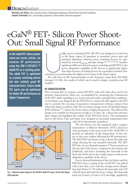
A test fixture was designed for the EPC2012 to connect the RF signals to the FET<br />
and to provide the necessary S-parameter measurement reference planes from<br />
which the dataset would be valid. The test fixture design used a 30 mil thick Rogers<br />
4350 substrate [21] , chosen for its low losses at higher frequencies. This allowed the<br />
design to be suitable for frequencies as high as 12 GHz. Fig. 1 shows the reference<br />
plane design and highlights the outline of the EPC2012 device. The transmission<br />
lines to the device Gate and Drain were designed as microstrip transmission lines<br />
with 50 Ω characteristic impedance.<br />
271<br />
914<br />
1621<br />
Drain Circuit<br />
Reference Plane<br />
Fig. 1. Reference plane design for the EPC2012 eGaN FET using a 30 mil thick Rogers<br />
4350 substrate.<br />
The test fixture was also equipped with a negative<br />
temperature co-efficient thermistor (NTC) placed in<br />
close proximity to the source pad of the eGaN FET to<br />
provide an indication of the temperature of the copper<br />
in that area without affecting the RF performance.<br />
The EPC9903 test fixture in Fig. 2 shows the right side<br />
image showing the top mounted heat-sink. The EPC<br />
FET has a lower thermal resistance [3] from junction to<br />
the top side of the device, compared to the bottom side<br />
(soldered), and hence mounting the heat-sink to the<br />
back side of the device has a high impact on the power<br />
dissipation capability of the device.<br />
Due to thermal limitations of the test fixture and the<br />
EPC2012 device, testing of the eGaN FET was pulsed<br />
with a low duty cycle with the average power dissipation<br />
kept below 0.7 W without the heat-sink, and 5 W<br />
with the heat-sink and forced air cooling. The heat-sink<br />
used was 15 mm x 15 mm x 14.5 mm high, supplied by<br />
www.powerelectronics.com June 2013 | <strong>Power</strong> <strong>Electronics</strong> <strong>Technology</strong> 19