Power Electronics Technology
Power Electronics Technology
Power Electronics Technology

You also want an ePaper? Increase the reach of your titles
YUMPU automatically turns print PDFs into web optimized ePapers that Google loves.
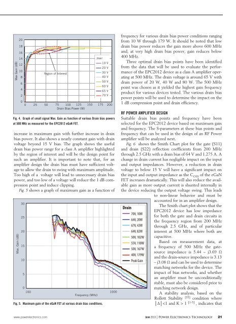
Max Gain (dB)<br />
20<br />
18<br />
16<br />
14<br />
12<br />
10<br />
8<br />
6<br />
4<br />
2<br />
0<br />
Region of Interest<br />
Drain<br />
10 V<br />
20 V<br />
30 V<br />
40 V<br />
50 V<br />
60 V<br />
65 V<br />
70 V<br />
0 25 50 75 100 125 150 175 200<br />
Drain Bias <strong>Power</strong> (W)<br />
Fig. 4. Graph of small signal Max. Gain as function of various Drain bias powers<br />
at 500 MHz as measured for the EPC2012 eGaN FET.<br />
increase in maximum gain with further increase in drain<br />
bias power. It also shows a nearly constant gain with drain<br />
voltage beyond 15 V bias. The graph shows the useful<br />
drain bias power range for a class A amplifier highlighted<br />
by the region of interest and will be the design point for<br />
such an amplifier. It is important to note that, for an<br />
amplifier design the drain bias must have sufficient voltage<br />
to allow the drain to swing with maximum amplitude.<br />
Too high of a voltage will lead to unnecessary drain bias<br />
power, and too low of a voltage will reduce the 1 dB compression<br />
point and induce clipping.<br />
Fig. 5 shows a graph of maximum gain as a function of<br />
Max. Gain (dB)<br />
30<br />
25<br />
20<br />
15<br />
10<br />
5<br />
0<br />
100 1000<br />
Frequency (MHz)<br />
Fig. 5. Maximum gain of the eGaN FET at various drain bias conditions.<br />
frequency for various drain bias power conditions ranging<br />
from 10 W through 179 W. It should be noted that low<br />
drain bias power reduces the gain more above 600 MHz<br />
and, at very high drain bias power, gain reduces below<br />
400 MHz.<br />
Three optimal drain bias points have been identified<br />
from the data that will be used to evaluate the performance<br />
of the EPC2012 device as a class A amplifier operating<br />
at 500 MHz. The drain voltage is around 65 V with<br />
drain power of 20 W, 40 W and 80 W. The 500 MHz<br />
point was chosen as it yielded the highest gain frequency<br />
product for various devices tested. The various drain bias<br />
power points will be used to determine the impact on the<br />
1 dB compression point and drain efficiency.<br />
RF POWER AMPLIFIER DESIGN<br />
Suitable drain bias points and frequency have been<br />
selected for the EPC2012 device based on maximum gain<br />
and frequency. The S-parameters at these bias points and<br />
frequency that can be used in the design of an RF <strong>Power</strong><br />
amplifier will be analyzed next.<br />
Fig. 6 shows the Smith Chart plot for the gate (S11)<br />
and drain (S22) reflection coefficients from 200 MHz<br />
through 2.5 GHz with a drain bias of 64 V and 1.275 A. A<br />
change in drain current has negligible impact on the input<br />
and output impedances. However, a reduction in drain<br />
voltage to below 15 V will have a significant impact on<br />
the input and output impedance as the COSS of the eGaN<br />
FET increases dramatically. This will also reduce the available<br />
gain as more output current is shunted internally in<br />
the device reducing the output voltage swing. This leads<br />
to non-linear behavior and must be<br />
accounted for in an amplifier design.<br />
The Smith chart plot shows that the<br />
EPC2012 device has low impedance<br />
for both the gate and drain circuits in<br />
the frequency region from 200 MHz<br />
through 2.5 GHz, and of particular<br />
interest at 500 MHz where both are<br />
capacitive.<br />
Based on measurement data, at<br />
a frequency of 500 MHz the gatesource<br />
impedance is 5.44 – j3.69 Ω<br />
and the drain-source impedance is 3.13<br />
– j3.08 Ω and can be used to determine<br />
matching networks for the device. The<br />
impact of bias networks, and whether<br />
an amplifier must be unconditionally<br />
stable, must also be considered prior to<br />
matching network design.<br />
A stability analysis, based on the<br />
Rollett Stability [22] condition where<br />
1 [1-5] Drain<br />
70 V, 10 W<br />
64 V, 20 W<br />
67 V, 43 W<br />
64 V, 82 W<br />
50 V, 102 W<br />
55 V, 118 W<br />
50 V, 167 W<br />
40 V, 179 W<br />
Peak Gain<br />
, indicates that<br />
www.powerelectronics.com June 2013 | <strong>Power</strong> <strong>Electronics</strong> <strong>Technology</strong> 21