1747-6.22, Backup Scanner User Manual
1747-6.22, Backup Scanner User Manual
1747-6.22, Backup Scanner User Manual

Create successful ePaper yourself
Turn your PDF publications into a flip-book with our unique Google optimized e-Paper software.
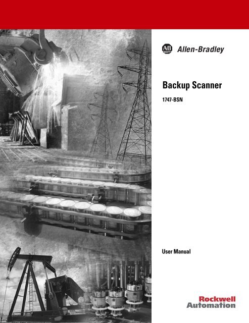
<strong>Backup</strong> <strong>Scanner</strong><br />
<strong>1747</strong>-BSN<br />
<strong>User</strong> <strong>Manual</strong>
Important <strong>User</strong> Information<br />
Because of the variety of uses for the products described in this<br />
publication, those responsible for the application and use of this<br />
control equipment must satisfy themselves that all necessary steps<br />
have been taken to assure that each application and use meets all<br />
performance and safety requirements, including any applicable laws,<br />
regulations, codes and standards.<br />
The illustrations, charts, sample programs and layout examples<br />
shown in this guide are intended solely for purposes of example.<br />
Since there are many variables and requirements associated with any<br />
particular installation, Allen-Bradley does not assume responsibility<br />
or liability (to include intellectual property liability) for actual use<br />
based upon the examples shown in this publication.<br />
Allen-Bradley publication SGI-1.1, Safety Guidelines for the<br />
Application, Installation and Maintenance of Solid-State Control<br />
(available from your local Allen-Bradley office), describes some<br />
important differences between solid-state equipment and<br />
electromechanical devices that should be taken into consideration<br />
when applying products such as those described in this publication.<br />
Reproduction of the contents of this copyrighted publication, in<br />
whole or part, without written permission of Allen-Bradley Company,<br />
Inc., is prohibited.<br />
Throughout this manual we use notes to make you aware of safety<br />
considerations:<br />
!<br />
ATTENTION: Identifies information about<br />
practices or circumstances that can lead to personal<br />
injury or death, property damage or economic loss.<br />
Attention statements help you to:<br />
• identify a hazard<br />
• avoid a hazard<br />
• recognize the consequences<br />
Important: Identifies information that is critical for successful<br />
application and understanding of the product.<br />
Publication <strong>1747</strong>-<strong>6.22</strong>
Overview<br />
Table of Contents<br />
Preface<br />
Who Should Use This <strong>Manual</strong> . . . . . . . . . . . . . . . . . . . . . . . . . P-1<br />
How to Use This <strong>Manual</strong> . . . . . . . . . . . . . . . . . . . . . . . . . . . . . P-1<br />
<strong>Manual</strong> Contents . . . . . . . . . . . . . . . . . . . . . . . . . . . . . . . . . P-1<br />
Related Documentation . . . . . . . . . . . . . . . . . . . . . . . . . . . . P-2<br />
Conventions Used in This <strong>Manual</strong> . . . . . . . . . . . . . . . . . . . . . . P-3<br />
Allen-Bradley Support . . . . . . . . . . . . . . . . . . . . . . . . . . . . . . . P-3<br />
Local Product Support . . . . . . . . . . . . . . . . . . . . . . . . . . . . . P-3<br />
Technical Product Assistance . . . . . . . . . . . . . . . . . . . . . . . P-3<br />
Your Questions or Comments on the <strong>Manual</strong> . . . . . . . . . . . P-3<br />
Chapter 1<br />
System Overview . . . . . . . . . . . . . . . . . . . . . . . . . . . . . . . . . . . 1-1<br />
<strong>Scanner</strong> I/O Image Division . . . . . . . . . . . . . . . . . . . . . . . . . 1-3<br />
How the <strong>Scanner</strong> Scans Remote I/O . . . . . . . . . . . . . . . . . . . . 1-4<br />
SLC and <strong>Scanner</strong> Asynchronous Operation . . . . . . . . . . . . . . 1-5<br />
How the <strong>Scanner</strong> Interacts with Adapters . . . . . . . . . . . . . . . . 1-6<br />
<strong>Scanner</strong> I/O Image Concepts. . . . . . . . . . . . . . . . . . . . . . . . 1-6<br />
Example <strong>Scanner</strong> I/O Image. . . . . . . . . . . . . . . . . . . . . . 1-7<br />
Transferring Data with RIO Discrete and Block Transfers 1-8<br />
Physical and Logical RIO Link Specifications. . . . . . . . . 1-9<br />
Extended Node Capability . . . . . . . . . . . . . . . . . . . . . . . 1-9<br />
Complementary I/O. . . . . . . . . . . . . . . . . . . . . . . . . . . . . 1-9<br />
Guidelines for Configuring Complementary I/O . . . . . . 1-10<br />
Complementary I/O: Placing Modules with<br />
2-Slot Addressing . . . . . . . . . . . . . . . . . . . . . . . . . . 1-11<br />
Complementary I/O: Placing Modules with<br />
1-Slot Addressing . . . . . . . . . . . . . . . . . . . . . . . . . . 1-12<br />
Complementary I/O: Placing Modules with 1/2-Slot<br />
Addressing . . . . . . . . . . . . . . . . . . . . . . . . . . . . . . . . 1-13<br />
Summary for Placing Modules Used In<br />
Complementary I/O . . . . . . . . . . . . . . . . . . . . . . . . . 1-13<br />
Discrete Modules . . . . . . . . . . . . . . . . . . . . . . . . . . . . . 1-13<br />
Block Transfer Modules. . . . . . . . . . . . . . . . . . . . . . . . . 1-14<br />
Complementary I/O Application Considerations . . . . . . 1-16<br />
Complementary 1771 I/O Module Details. . . . . . . . . . . 1-16<br />
Hardware Features . . . . . . . . . . . . . . . . . . . . . . . . . . . . . . 1-17<br />
Status LEDs . . . . . . . . . . . . . . . . . . . . . . . . . . . . . . . . . . . . 1-17<br />
Configuration Dip Switch Settings . . . . . . . . . . . . . . . . . . . 1-18<br />
Module Address Switch . . . . . . . . . . . . . . . . . . . . . . . . 1-19<br />
Compatible Devices . . . . . . . . . . . . . . . . . . . . . . . . . . . 1-19<br />
<strong>Backup</strong> Concepts for the SLC 500 System . . . . . . . . . . . . . . 1-20<br />
Why Use a <strong>Backup</strong> System? . . . . . . . . . . . . . . . . . . . . 1-20<br />
Applying <strong>1747</strong>-BSN <strong>Backup</strong> <strong>Scanner</strong> Modules<br />
to the SLC-500 Programmable Controller . . . . . . . . 1-20<br />
A Typical SLC 500 <strong>Backup</strong> Configuration . . . . . . . . . . . 1-21<br />
Publication <strong>1747</strong>-<strong>6.22</strong>
vi Table of Contents<br />
Publication <strong>1747</strong>-<strong>6.22</strong><br />
How the SLC 500 <strong>Backup</strong> System Works. . . . . . . . 1-22<br />
Chapter 2<br />
Quick Start for Experienced <strong>User</strong>s<br />
Required Tools and Equipment . . . . . . . . . . . . . . . . . . . . . 2-1<br />
Procedures . . . . . . . . . . . . . . . . . . . . . . . . . . . . . . . . . . . . . 2-2<br />
Installation and Wiring<br />
Operating Your SLC 500<br />
<strong>Backup</strong> System<br />
Chapter 3<br />
Compliance to European Union Directives . . . . . . . . . . 3-1<br />
EMC Directive . . . . . . . . . . . . . . . . . . . . . . . . . . . . . . . . 3-1<br />
Configuration Selection . . . . . . . . . . . . . . . . . . . . . . . . . . . 3-1<br />
Baud Rate Settings. . . . . . . . . . . . . . . . . . . . . . . . . . 3-2<br />
Module Address Switch . . . . . . . . . . . . . . . . . . . . . . 3-2<br />
<strong>Backup</strong> <strong>Scanner</strong> Installation . . . . . . . . . . . . . . . . . . . . . 3-3<br />
Insertion . . . . . . . . . . . . . . . . . . . . . . . . . . . . . . . . . . 3-3<br />
Removal . . . . . . . . . . . . . . . . . . . . . . . . . . . . . . . . . . 3-4<br />
Wiring. . . . . . . . . . . . . . . . . . . . . . . . . . . . . . . . . . . . . . . 3-4<br />
Terminal Wiring . . . . . . . . . . . . . . . . . . . . . . . . . . . . . 3-4<br />
Status LEDs . . . . . . . . . . . . . . . . . . . . . . . . . . . . . . . 3-6<br />
Chapter 4<br />
Chapter Objectives . . . . . . . . . . . . . . . . . . . . . . . . . . . . . . . 4-1<br />
How the <strong>1747</strong>-BSN Module Operates . . . . . . . . . . . . . . . . 4-1<br />
Automatic Transfer of Remote Input Data<br />
Over the HSSL . . . . . . . . . . . . . . . . . . . . . . . . . . . . . 4-1<br />
RS-232/485 Communication Channel . . . . . . . . . . . 4-2<br />
RIO/DH+ Communication Channel. . . . . . . . . . . . . . 4-2<br />
Secondary Processor Remote Programming . . . . . . 4-4<br />
Data Table Transfer . . . . . . . . . . . . . . . . . . . . . . . . . . . . . . 4-5<br />
How the <strong>Backup</strong> System Operates . . . . . . . . . . . . . . . . . . 4-5<br />
Primary Program . . . . . . . . . . . . . . . . . . . . . . . . . . . . . . 4-6<br />
Secondary Program . . . . . . . . . . . . . . . . . . . . . . . . . . . . 4-6<br />
<strong>Backup</strong> System Theory of Operation . . . . . . . . . . . . . . . 4-6<br />
Startup Sequencing . . . . . . . . . . . . . . . . . . . . . . . . . 4-7<br />
Power-up Sequencing . . . . . . . . . . . . . . . . . . . . . . . . . . . . 4-7<br />
Processor Mode Change Sequencing . . . . . . . . . . . . . . . . 4-7<br />
Fail-over Sequencing . . . . . . . . . . . . . . . . . . . . . . . . . . . . . 4-8<br />
Power Down Sequencing . . . . . . . . . . . . . . . . . . . . . . . . . . 4-8<br />
Restarting a failed system . . . . . . . . . . . . . . . . . . . . . . . . . 4-8
<strong>Scanner</strong> Configuration and<br />
Programming<br />
Module Control and Status<br />
Word<br />
Chapter 5<br />
Table of Contents vii<br />
Understanding Remote Input and Output Image Files . . . 5-1<br />
RIO Configuration Using G Files . . . . . . . . . . . . . . . . . . 5-2<br />
Rules for Configuring the <strong>Scanner</strong> . . . . . . . . . . . . . . . . . . . 5-5<br />
General . . . . . . . . . . . . . . . . . . . . . . . . . . . . . . . . . . . . . 5-5<br />
Concerning Complementary I/O . . . . . . . . . . . . . . . 5-5<br />
Considerations When Configuring Remote I/O . . . . . . . . . 5-9<br />
G File Considerations . . . . . . . . . . . . . . . . . . . . . . . . . . 5-9<br />
Crossing Logical Rack Boundaries . . . . . . . . . . . . . . . . . . 5-9<br />
Examples of Crossing Logical Rack Boundaries. . . . . . 5-9<br />
Understanding M Files . . . . . . . . . . . . . . . . . . . . . . . . . . . 5-10<br />
M Files Overview. . . . . . . . . . . . . . . . . . . . . . . . . . . . . 5-10<br />
M0 Control File Description . . . . . . . . . . . . . . . . . . . . . 5-13<br />
M0 File - RIO Device Inhibit Control . . . . . . . . . . . . . . . . 5-14<br />
M0 File - RIO Device Reset Control . . . . . . . . . . . . . . . . 5-15<br />
M0 File - Remote Output Reset Control . . . . . . . . . . . . . 5-16<br />
Device Reset and Remote Output Reset<br />
Considerations From this mode . . . . . . . . . . . . 5-17<br />
M1 Status File Description . . . . . . . . . . . . . . . . . . . . . . . . 5-19<br />
General Communication Status - Enable Device<br />
Fault Bit . . . . . . . . . . . . . . . . . . . . . . . . . . . . . . . . . . . . . . 5-19<br />
General Communication Status - Communication<br />
Attempted Bit . . . . . . . . . . . . . . . . . . . . . . . . . . . . . . . . . 5-20<br />
RIO Baud Rate Status . . . . . . . . . . . . . . . . . . . . . . . . . . . 5-20<br />
Logical Device Starting Address Status . . . . . . . . . . . . . . 5-21<br />
Logical Device Image Size Status . . . . . . . . . . . . . . . . . . 5-21<br />
Active Device Status . . . . . . . . . . . . . . . . . . . . . . . . . . . . 5-22<br />
Logical Device Fault Status . . . . . . . . . . . . . . . . . . . . . . . 5-23<br />
RIO Status Example . . . . . . . . . . . . . . . . . . . . . . . . . . . . 5-25<br />
SLC/<strong>Scanner</strong> Configuration . . . . . . . . . . . . . . . . . . . . . . . 5-29<br />
Chapter 6<br />
System Status Word . . . . . . . . . . . . . . . . . . . . . . . . . . . . . 6-2<br />
Module Status Word . . . . . . . . . . . . . . . . . . . . . . . . . . . . . 6-4<br />
Transferring Data over the High-Speed Serial Link<br />
(HSSL) . . . . . . . . . . . . . . . . . . . . . . . . . . . . . . . . . . . . . . . 6-5<br />
Data Transfer Control Word . . . . . . . . . . . . . . . . . . . . . . . . 6-6<br />
Data Transfer Status Word . . . . . . . . . . . . . . . . . . . . . . . . 6-7<br />
Data Transfer Handshake Word . . . . . . . . . . . . . . . . . . . . 6-8<br />
Program File 2 . . . . . . . . . . . . . . . . . . . . . . . . . . . . . 6-9<br />
Publication <strong>1747</strong>-<strong>6.22</strong>
viii Table of Contents<br />
RIO Block Transfer<br />
Publication <strong>1747</strong>-<strong>6.22</strong><br />
Program File 3 . . . . . . . . . . . . . . . . . . . . . . . . . . . . 6-10<br />
Program File 4 . . . . . . . . . . . . . . . . . . . . . . . . . . . . 6-11<br />
Switch Assemblies Status Word . . . . . . . . . . . . . . . . . . . . 6-12<br />
Module Status Counters . . . . . . . . . . . . . . . . . . . . . . . . . . 6-13<br />
Data Block Counters . . . . . . . . . . . . . . . . . . . . . . . . . . . . 6-14<br />
Chapter 7<br />
RIO Block Transfer Theory of Operation . . . . . . . . . . . . . . 7-1<br />
What Is RIO Block Transfer? . . . . . . . . . . . . . . . . . . . . . 7-1<br />
RIO Block Transfer General Functional Overview . . . . . . . 7-5<br />
<strong>Scanner</strong> I/O Image Allocation For Block Transfer . . . . . 7-6<br />
Examples of BT I/O Image File Allocation . . . . . . . . . . . 7-6<br />
<strong>Scanner</strong>’s Block Transfer Buffer Layout . . . . . . . . . . . . . . . 7-8<br />
M0 File - Block Transfer Output/Control Buffers . . . . . . 7-8<br />
M0 File BT Control Buffer Layout . . . . . . . . . . . . . . . 7-9<br />
BT Control Flag Definitions . . . . . . . . . . . . . . . . . . . 7-9<br />
M1 File - Block Transfer Input/Status Buffers . . . . . . . . 7-9<br />
M1 File - Input/Status BT Buffer Layout<br />
(M1:e.100... M1:e.3200). . . . . . . . . . . . . . . . . . . 7-10<br />
M1 File - BTR/BTW Error Codes (M1:e.103 ...<br />
M1:e.3203) . . . . . . . . . . . . . . . . . . . . . . . . . . . . . 7-10<br />
M1 File - BTR/BTW Status Flag Definitions<br />
(M1:e.100 ... M1:e.3200) . . . . . . . . . . . . . . . . . . 7-11<br />
Detailed Operation of RIO Block Transfer . . . . . . . . . . . . 7-12<br />
Block Transfer Timing Diagrams . . . . . . . . . . . . . . . . . 7-14<br />
Successful Block Transfer. . . . . . . . . . . . . . . . . . . . 7-14<br />
Successful Block Transfer Read/Write . . . . . . . . . . 7-14<br />
Block Transfer Failure at Startup. . . . . . . . . . . . . . . 7-15<br />
Block Transfer Failure at Startup. . . . . . . . . . . . . . . 7-15<br />
Block Transfer Failure After Startup of<br />
Transmission Across RIO Link . . . . . . . . . . . . . . 7-16<br />
Block Transfer Failure after Startup of<br />
Transmission Across the RIO Link . . . . . . . . . . . 7-16<br />
SLC Control Program Cancelling a Block<br />
Transfer Once Transmitted Across RIO Link . . . 7-17<br />
SLC Control Program Canceling a BT Once<br />
Transmitted Across RIO Link . . . . . . . . . . . . . . . 7-17<br />
SLC Control Program Cancelling a Block<br />
Transfer Prior To Transmission Across RIO Link 7-18<br />
SLC Control Program Canceling a BT Prior to<br />
Transmission Across RIO Link . . . . . . . . . . . . . . 7-18<br />
Setting Up A Block Transfer . . . . . . . . . . . . . . . . . . . . . . . 7-20<br />
Quick Reference to Status and Control Bits . . . . . . . . . . . 7-20<br />
Status Bits. . . . . . . . . . . . . . . . . . . . . . . . . . . . . . . . 7-20<br />
Control Bits . . . . . . . . . . . . . . . . . . . . . . . . . . . . . . . 7-21<br />
Block Transfer Read Control Logic Example . . . . . . . . . . 7-21<br />
Directional Continuous Block Transfer Example . . . . . 7-27<br />
Directional Repeating Block Transfer Example . . . . . . 7-31
Switchover Considerations<br />
Programming Techniques<br />
Chapter 8<br />
Table of Contents ix<br />
Directional Non-Continuous Block Transfer<br />
Example . . . . . . . . . . . . . . . . . . . . . . . . . . . . . . 7-34<br />
Bidirectional Continuous Block Transfer Example . 7-37<br />
Bidirectional Alternating Block Transfer . . . . . . . . . 7-42<br />
Bidirectional Alternating Repeating Block Transfer 7-48<br />
Timing Requirements . . . . . . . . . . . . . . . . . . . . . . . . . . . . . 8-1<br />
Input Signal Update Time . . . . . . . . . . . . . . . . . . . . . . . 8-2<br />
Time-out on Remote I/O Link . . . . . . . . . . . . . . . . . . . . 8-2<br />
Data Table Transfer Time on HSSL . . . . . . . . . . . . . . . 8-2<br />
Divergence . . . . . . . . . . . . . . . . . . . . . . . . . . . . . . . . . . . . . 8-3<br />
Forcing I/O . . . . . . . . . . . . . . . . . . . . . . . . . . . . . . . . . . . . . 8-3<br />
Data Highway Plus Switching . . . . . . . . . . . . . . . . . . . . . . 8-4<br />
Remote I/O Switching . . . . . . . . . . . . . . . . . . . . . . . . . . . . 8-6<br />
Chapter 9<br />
Chapter Objectives . . . . . . . . . . . . . . . . . . . . . . . . . . . . . . 9-1<br />
Getting Started . . . . . . . . . . . . . . . . . . . . . . . . . . . . . . . . . . 9-1<br />
Program File 2 . . . . . . . . . . . . . . . . . . . . . . . . . . . . . 9-2<br />
Program File 3 . . . . . . . . . . . . . . . . . . . . . . . . . . . . . 9-3<br />
Program File 4 . . . . . . . . . . . . . . . . . . . . . . . . . . . . . 9-8<br />
Data Transfer Schemes . . . . . . . . . . . . . . . . . . . . . . . . . . 9-13<br />
Data Transfer Method 1. . . . . . . . . . . . . . . . . . . . . . . . 9-13<br />
Data Transfer Method 2. . . . . . . . . . . . . . . . . . . . . . . . 9-14<br />
Other transfer methods . . . . . . . . . . . . . . . . . . . . . . . . 9-15<br />
Accounting for Instructions That Could Cause<br />
Problems During Switchover . . . . . . . . . . . . . . . . . . . . . 9-16<br />
Timer Instructions . . . . . . . . . . . . . . . . . . . . . . . . . . . . 9-16<br />
Counter Instructions . . . . . . . . . . . . . . . . . . . . . . . . . . 9-17<br />
Programming Techniques . . . . . . . . . . . . . . . . . . . . . . 9-18<br />
Diagnostic, Sequencing, File Arithmetic and Logic<br />
File Search and Compare, File Copy<br />
and Fill Instructions. . . . . . . . . . . . . . . . . . . . . . . . . 9-18<br />
FIFO and Bit Displacement Instructions . . . . . . . . . . . 9-18<br />
Block Transfer Instructions . . . . . . . . . . . . . . . . . . . . . 9-19<br />
Message Instructions. . . . . . . . . . . . . . . . . . . . . . . . . . 9-19<br />
PID Control Files . . . . . . . . . . . . . . . . . . . . . . . . . . . . . 9-20<br />
Summary of Programming Considerations . . . . . . . . . . . 9-20<br />
Publication <strong>1747</strong>-<strong>6.22</strong>
x Table of Contents<br />
Specifications<br />
M0-M1 Files and G Files<br />
Publication <strong>1747</strong>-<strong>6.22</strong><br />
Appendix A<br />
<strong>Backup</strong> <strong>Scanner</strong> Operating Specifications . . . . . . . . . . . . .A-1<br />
Network Specifications . . . . . . . . . . . . . . . . . . . . . . . . . . . .A-1<br />
Throughput Introduction . . . . . . . . . . . . . . . . . . . . . . . . . . .A-2<br />
RIO Network Throughput Components . . . . . . . . . . . . .A-2<br />
Calculating Throughput . . . . . . . . . . . . . . . . . . . . . . . . . . .A-3<br />
Discrete I/O Throughput without Block Transfers<br />
(Tdm-nbt) Present. . . . . . . . . . . . . . . . . . . . . . . . . . .A-3<br />
RIO Scan Time Calculation (TRIO) . . . . . . . . . . . . . . . .A-4<br />
Example Discrete I/O Throughput without Block<br />
Transfers Present. . . . . . . . . . . . . . . . . . . . . . . . . . . .A-4<br />
Discrete I/O Throughput with Block Transfers<br />
(Tdm-bt) Present. . . . . . . . . . . . . . . . . . . . . . . . . . . .A-6<br />
Determining TSNo-bt . . . . . . . . . . . . . . . . . . . . . . . .A-6<br />
Determining Tbtx . . . . . . . . . . . . . . . . . . . . . . . . . . .A-7<br />
Example Discrete I/O Throughput with Block Transfers<br />
Present. . . . . . . . . . . . . . . . . . . . . . . . . . . . . . . . . . . .A-7<br />
Block Transfer Throughput. . . . . . . . . . . . . . . . . . . . . . .A-9<br />
<strong>Backup</strong> <strong>Scanner</strong> Output Delay Time (TSNo) Tables . .A-11<br />
Determining the Number of Logical Racks<br />
Configured . . . . . . . . . . . . . . . . . . . . . . . . . . . . .A-11<br />
Appendix B<br />
M0-M1 Files . . . . . . . . . . . . . . . . . . . . . . . . . . . . . . . . . . . .B-1<br />
Configuring M0-M1 Files . . . . . . . . . . . . . . . . . . . . . . . .B-1<br />
Addressing M0-M1 Files . . . . . . . . . . . . . . . . . . . . . . . .B-2<br />
Using M0-M1 Data File Addresses . . . . . . . . . . . . . . . .B-2<br />
Monitoring Bit Addresses . . . . . . . . . . . . . . . . . . . . . . . .B-3<br />
M0/M1 Monitoring Option Disabled . . . . . . . . . . . . . . . .B-3<br />
M0/M1 Monitoring Option Enabled. . . . . . . . . . . . . . . . .B-4<br />
Transferring Data Between Processor Files<br />
and M0 or M1 Files . . . . . . . . . . . . . . . . . . . . . . . . . .B-4<br />
Access Time . . . . . . . . . . . . . . . . . . . . . . . . . . . . . . . . .B-5<br />
SLC 5/02 Processor Example. . . . . . . . . . . . . . . . . .B-5<br />
SLC 5/03 Processor Example. . . . . . . . . . . . . . . . . .B-6<br />
SLC 5/04 Processor Example. . . . . . . . . . . . . . . . . .B-6<br />
Minimizing the Scan Time . . . . . . . . . . . . . . . . . . . . . . .B-6<br />
Capturing M0-M1 File Data . . . . . . . . . . . . . . . . . . . . . .B-7<br />
Specialty I/O Modules with Retentive Memory. . . . . . . .B-8<br />
G Files . . . . . . . . . . . . . . . . . . . . . . . . . . . . . . . . . . . . . . . .B-8<br />
Configuring G Files . . . . . . . . . . . . . . . . . . . . . . . . . .B-9<br />
Editing G File Data. . . . . . . . . . . . . . . . . . . . . . . . . . . .B-10
Glossary<br />
Index<br />
Table of Contents xi<br />
Appendix C<br />
RIO Configuration Worksheet . . . . . . . . . . . . . . . . . . . . C-1<br />
Directions . . . . . . . . . . . . . . . . . . . . . . . . . . . . . . . . . . . . . . C-1<br />
Publication <strong>1747</strong>-<strong>6.22</strong>
xii Table of Contents<br />
Publication <strong>1747</strong>-<strong>6.22</strong>
Who Should Use This<br />
<strong>Manual</strong><br />
How to Use This<br />
<strong>Manual</strong><br />
Preface<br />
Read this preface to familiarize yourself with the rest of the manual.<br />
This preface covers the following topics:<br />
• who should use this manual<br />
• how to use this manual<br />
• related publications<br />
• conventions used in this manual<br />
• Allen-Bradley support<br />
Use this manual if you are responsible for designing, installing,<br />
programming, or troubleshooting control systems that use<br />
Allen-Bradley small logic controllers.<br />
As much as possible, we organized this manual to explain, in a taskby-task<br />
manner, how to install, configure, program, operate and<br />
troubleshoot a control system using the <strong>1747</strong>-BSN <strong>Backup</strong> <strong>Scanner</strong>.<br />
<strong>Manual</strong> Contents<br />
If you want... See<br />
An overview of the system including backup scanner/SLC interaction, compatible devices, and features Chapter 1<br />
A quick start guide for experienced users Chapter 2<br />
Installation and wiring guidelines Chapter 3<br />
Operating your SLC 500 backup system Chapter 4<br />
<strong>Backup</strong> scanner configuration information, I/O file information, and G and M file descriptions Chapter 5<br />
Information on module control and status word Chapter 6<br />
RIO block transfer information, M file block transfer buffer layout, block transfer examples Chapter 7<br />
Switchover considerations Chapter 8<br />
Programming techniques Chapter 9<br />
<strong>Backup</strong> scanner and system specifications Appendix A<br />
Information and usage of M and G files Appendix B<br />
Worksheets for configuring the scanner’s I/O image Appendix C<br />
Definitions of terms used in this manual Glossary<br />
Publication <strong>1747</strong>-<strong>6.22</strong>
14<br />
Publication <strong>1747</strong>-<strong>6.22</strong><br />
Related Documentation<br />
The table below provides a listing of publications that contain<br />
important information about Allen-Bradley SLC products.<br />
For Read this document Document number<br />
An overview of the SLC 500 family of products SLC 500 System Overview <strong>1747</strong>-2.30<br />
A description on how to install and use your Modular SLC 500<br />
programmable controller<br />
A reference manual that contains status file data and instruction set<br />
information for the SLC 500 processors.<br />
Installation guide for the <strong>Backup</strong> <strong>Scanner</strong> Module<br />
Installation & Operation <strong>Manual</strong> for<br />
Modular Hardware Style Programmable<br />
Controllers<br />
SLC 500 and MicroLogix 1000<br />
Instruction Set Reference <strong>Manual</strong><br />
<strong>Backup</strong> <strong>Scanner</strong> Module Installation<br />
Instructions<br />
An article on wire sizes and types for grounding electrical equipment National Electrical Code<br />
A complete listing of current Allen-Bradley documentation, including<br />
ordering instructions. Also indicates whether the documents are<br />
available on CD-ROM or in multi-languages.<br />
A glossary of industrial automation terms and abbreviations<br />
In-depth information on grounding and wiring Allen-Bradley<br />
programmable controllers.<br />
<strong>1747</strong>-6.2<br />
<strong>1747</strong>-6.15<br />
<strong>1747</strong>-5.38<br />
Published by the<br />
National Fire Protection<br />
Association of Boston,<br />
MA.<br />
Allen-Bradley Publication Index SD499<br />
Allen-Bradley Industrial Automation<br />
Glossary<br />
Allen-Bradley Programmable Controller<br />
Grounding and Wiring Guidelines<br />
AG-7.1<br />
1770-4.1<br />
If you would like a manual, you can:<br />
• download a free electronic version from the internet at<br />
www.theautomationbookstore.com<br />
• purchase a printed manual by:<br />
– contacting your local distributor or Rockwell Automation<br />
representative<br />
– visiting www.theautomationbookstore.com and placing<br />
your order<br />
– calling 1.800.963.9548 (USA/Canada) or 001.330.725.1574<br />
(Outside USA/Canada)
Conventions Used in<br />
This <strong>Manual</strong><br />
The following conventions are used throughout this manual:<br />
• Bulleted lists (like this one) provide information not procedural<br />
steps.<br />
• Numbered lists provide sequential steps or hierarchical<br />
information.<br />
• Italic type is used for emphasis.<br />
• Text in this font indicates words or phrases you should type.<br />
Allen-Bradley Support Allen-Bradley offers support services worldwide, with over 75 Sales/<br />
Support Offices, 512 authorized distributors and 260 authorized<br />
Systems Integrators located throughout the United States alone, plus<br />
Allen-Bradley representatives in every major country in the world.<br />
Local Product Support<br />
Contact your local Allen-Bradley representative for:<br />
• sales and order support<br />
• product technical training<br />
• warranty support<br />
• support service agreement<br />
Technical Product Assistance<br />
If you need to contact Allen-Bradley for technical assistance, please<br />
review the information in Chapter 6, Module Diagnostics and<br />
Troubleshooting first. Then call your local Allen-Bradley<br />
representative.<br />
Your Questions or Comments on the <strong>Manual</strong><br />
If you find a problem with this manual, please notify us using the selfmailer<br />
Publications Problem Report in the front of this manual.<br />
If you have any suggestions for how this manual could be made more<br />
useful to you, please contact us at the address below:<br />
Allen-Bradley Company, Inc.<br />
Control and Information Group<br />
Technical Communication, Dept. A602V, T122<br />
P.O. Box 2086<br />
Milwaukee, WI 53201-2086<br />
15<br />
Publication <strong>1747</strong>-<strong>6.22</strong>
16<br />
Publication <strong>1747</strong>-<strong>6.22</strong>
Overview<br />
This chapter contains the following information:<br />
• system overview<br />
• how the scanner interacts with the SLC processor<br />
• how the scanner interacts with adapter modules<br />
• scanner I/O image concepts<br />
• extended node capability<br />
• complementary I/O<br />
• scanner features<br />
• compatible network devices<br />
• backup concepts for the SLC-500 system<br />
Chapter 1<br />
System Overview The <strong>1747</strong>-BSN <strong>Backup</strong> <strong>Scanner</strong> provides redundancy for:<br />
• Remote I/O (RIO)<br />
• RS232 channel switchover for communications to devices such<br />
as operator interface<br />
• DH+<br />
The backup scanner also provides a High Speed Serial Link (HSSL)<br />
to write any retentative data from a primary to a secondary processor.<br />
In addition, the module has a Local Serial Link (LSL) to pass status<br />
information between multiple BSN modules located in the same<br />
chassis (optional).<br />
The <strong>1747</strong>-BSN is a complementary set of modules, with one module<br />
residing in the primary system and another module in the secondary<br />
or backup system. The primary module controls the operation of<br />
remote I/O, while the secondary module is available to take over<br />
control in the event of a fault in the primary.<br />
The backup scanner has the capability to switch between two<br />
communication channels. The first channel is configurable as RIO or<br />
DH+. The second channel is used to switch the RS232/485 channel in<br />
order to provide connection for electronic operator interfaces.<br />
The Remote I/O (RIO) scanner, Catalog Number <strong>1747</strong>-SN, is the<br />
remote I/O scanner for the SLC 500. It enables communication<br />
between an SLC processor (SLC 5/02 or later) and remotely located<br />
(3,048 meters [10,000 feet] maximum) 1746 I/O chassis and other<br />
RIO-compatible Allen-Bradley operator interface and control<br />
devices. The <strong>1747</strong>-SN scanner communicates with remotely located<br />
devices using the A-B Remote I/O link. The RIO link consists of a<br />
single master (scanner) and multiple slaves (adapters).<br />
Publication <strong>1747</strong>-<strong>6.22</strong>
1-18 Overview<br />
SLC 5/02 or<br />
later Processor<br />
Dataliner Message Display<br />
(Adapter/Slave)<br />
SLC 5/02 or<br />
Later Processor RIO <strong>Scanner</strong><br />
Half Logical<br />
Rack<br />
Device<br />
Publication <strong>1747</strong>-<strong>6.22</strong><br />
RIO <strong>Scanner</strong> (Master<br />
of the RIO LInk)<br />
Communication between devices occurs over twisted-pair cable with<br />
the devices daisy-chained together. The scanner can reside in any slot<br />
of the local SLC chassis except for slot 0. The <strong>1747</strong>-BSN includes the<br />
same functionality as the <strong>1747</strong>-SN scanner, as well as the backup<br />
features.<br />
The scanner transfers input and output data between<br />
itself and all configured network devices over twisted-pair<br />
cable. Note that the end-to-end length of the cable can be<br />
a maximum of 3,048 meters (10,000 feet)<br />
Local SLC Chassis Remote Chassis<br />
Quarter Logical<br />
Rack<br />
Device<br />
PanelView-Operator Terminal<br />
(Adapter/Slave)<br />
RediPANEL-<br />
(Adapter/Slave)<br />
<strong>1747</strong>-ASB Module (Adapter/<br />
Slave)<br />
Remote Expansion Chassis<br />
The scanner can be configured for and transfer a maximum of 4<br />
logical racks of discrete data on the RIO link. The scanner provides<br />
discrete I/O and block transfers. Configurations allowed are any<br />
combination of quarter, half, three quarter, or full logical rack<br />
devices.<br />
The scanner transfers discrete input and output data between itself,<br />
remote adapters, and the SLC processor. Remote adapters consist of<br />
1746 chassis and other Allen-Bradley operator interface and control<br />
devices.<br />
Adapter 1 Adapter 2 Adapter 3 Adapter 4 Adapter 5 Adapter 6<br />
Half<br />
Logical Rack<br />
Device<br />
Three Quarter<br />
Logical Rack Device<br />
Full<br />
Logical Rack<br />
Device<br />
Full<br />
Logical Rack<br />
Device
Local I/O<br />
Remote I/O<br />
Processor I/O Image<br />
Overview 1-19<br />
The SLC processor transfers the scanner’s 4 logical racks (32 input<br />
image and 32 output image words) of discrete remote I/O image data<br />
into the SLC input and output image files. You can adjust the size of<br />
the scanner input and output image file during configuration of your<br />
SLC system so that the scanner only transfers the discrete I/O data<br />
your application program requires. Configuration is done through the<br />
configuration file (G file). Refer to chapter 4, Configuration and<br />
Programming, for more information.<br />
Important: The SLC 500 processor (SLC 5/02 or later) supports<br />
multiple scanners in its local I/O chassis. The maximum<br />
number is dependent on the following:<br />
• backplane power requirements (power supply dependent)<br />
• SLC 500 processor I/O data table limit (4,096 I/O)<br />
Based on SLC processor I/O capacity only, a maximum of eight<br />
scanners may be used when no local I/O exists.<br />
• processor memory to support the application (SLC 500<br />
processor dependent)<br />
<strong>Scanner</strong> I/O Image Division<br />
The scanner allows each adapter to use a fixed amount (user-defined)<br />
of the scanner’s input and output image. Part of the SLC processor’s<br />
image is used by local I/O; the other portion is used by the scanner for<br />
remote I/O.<br />
The scanner remote I/O image is divided into logical racks and<br />
further divided into logical groups. A full logical rack consists of<br />
eight input and eight output image words. A logical group consists of<br />
one input and one output word in a logical rack. Each logical group is<br />
assigned a number from 0-7.<br />
Logical Rack 0<br />
Logical Rack 1<br />
Logical Rack 2<br />
Logical Group 0<br />
Logical Group 7<br />
<strong>Scanner</strong> I/O Image<br />
Adapter<br />
Image<br />
The scanner image contains the image of each adapter on the RIO<br />
link. The adapter is assigned a portion of the scanner image, which is<br />
referred to as the adapter image.<br />
Publication <strong>1747</strong>-<strong>6.22</strong>
1-20 Overview<br />
How the <strong>Scanner</strong><br />
Scans Remote I/O<br />
Publication <strong>1747</strong>-<strong>6.22</strong><br />
RIO <strong>Scanner</strong> Scan<br />
The scanner communicates with each logical device in a sequential<br />
fashion. First, the scanner initiates communication with a device by<br />
sending output data to the device. The device then responds by<br />
sending its input data back to the scanner, as illustrated below. You<br />
refer to this exchange as a discrete I/O transfer. After the scanner<br />
completes its discrete I/O transfer with the last configured network<br />
device, it begins another discrete I/O transfer with the first device.<br />
It is important to understand that the scanner transfers RIO data on a<br />
logical device basis not on an adapter basis. A logical device is a full<br />
logical rack or portion of a logical rack assigned to an adapter.<br />
The scanner updates its input image<br />
file each time it scans a logical device.<br />
<strong>Scanner</strong> Input<br />
Image File<br />
Input Device<br />
3<br />
Output Device<br />
3<br />
Output<br />
Device 2<br />
<strong>Scanner</strong> Output Image<br />
File<br />
Input<br />
Device 1<br />
Input Device<br />
2<br />
Output Device<br />
1
SLC and <strong>Scanner</strong><br />
Asynchronous<br />
Operation<br />
SLC Processor Scan Cycle<br />
The SLC processor reads the<br />
scanner input image file into the<br />
SLC input image file, processes<br />
it, and creates an SLC output<br />
image file. The SLC processor<br />
transfers its output file to the<br />
scanner.<br />
Program<br />
SLC Processor<br />
Overview 1-21<br />
The SLC processor scan and RIO scanner scan are independent<br />
(asynchronous) of each other. The SLC processor reads the scanner<br />
input image file during its input scan and writes the output image file<br />
to the scanner during its output scan. The RIO scanner continues<br />
reading inputs and writing outputs to the scanner I/O image file,<br />
independent of the SLC processor scan cycle.<br />
Depending on your SLC processor, RIO link configuration, and<br />
application program size, the scanner may complete multiple scans<br />
before the SLC processor reads the scanner’s input image file. The<br />
RIO scanner updates its I/O files on a per logical rack basis.<br />
The figure below illustrates the asynchronous operation of the SLC<br />
processor and RIO scanner.<br />
SLC Input<br />
Image File<br />
SLC Output<br />
Image file<br />
Output<br />
<strong>Scanner</strong> Image<br />
Input Device 3<br />
Image File<br />
Input<br />
Image<br />
Device 3<br />
<strong>Scanner</strong><br />
Output Image<br />
File<br />
Output<br />
Image<br />
Device 2<br />
Input<br />
Image<br />
Device 1<br />
Input<br />
Image<br />
Device 2<br />
Output<br />
Image<br />
Device 1<br />
RIO <strong>Scanner</strong> Scan Cycle<br />
The scanner updates its input<br />
image file each time it scans a<br />
logical device. The scanner<br />
may scan all of its configured<br />
logical devices several times<br />
before the SLC processor<br />
reads the scanner’s input<br />
image file<br />
Important: The outputs of the RIO are updated after the end of the<br />
first SLC processor scan.<br />
Publication <strong>1747</strong>-<strong>6.22</strong>
1-22 Overview<br />
How the <strong>Scanner</strong><br />
Interacts with<br />
Adapters<br />
SLC Local Chassis<br />
Publication <strong>1747</strong>-<strong>6.22</strong><br />
Processor <strong>Scanner</strong><br />
The scanner’s function is to continuously scan the adapters on the<br />
RIO link in a consecutive manner. This scan consists of one or more<br />
RIO discrete transfers to each adapter on the RIO link.<br />
RIO discrete transfers consist of the scanner sending output image<br />
data and communication commands to the adapter that instruct the<br />
adapter on how to control its output. (These include run, adapter reset,<br />
and reset decide commands.) The adapter responds by sending input<br />
data to the scanner. The scanner performs as many RIO discrete<br />
transfers as necessary to update the entire adapter image. If RIO<br />
discrete transfers do not occur, data is not exchanged between the<br />
scanner and adapter. RIO discrete transfers are asynchronous to the<br />
processor scan.<br />
RIO Discrete<br />
Transfers with<br />
Adapter 1<br />
RIO Discrete<br />
Transfers<br />
with Adapter 2<br />
RIO Discrete Transfers<br />
with Adapter 3<br />
RIO Discrete<br />
Transfers<br />
with Adapter 4<br />
<strong>Scanner</strong> I/O Image Concepts<br />
PanelView Operator Terminal<br />
RediPANEL<br />
The scanner’s I/O image consists of RIO logical racks and I/O<br />
groups. A full RIO logical rack consists of eight input image and<br />
eight output image words. (A word consists of 16 bits of data.) Each<br />
word within an RIO logical rack is assigned an I/O group number<br />
from 0 to 7.<br />
You assign devices on the RIO link a portion of the scanner’s image.<br />
Devices can occupy a quarter logical rack (2 input and output words),<br />
half logical rack (4 I/O words), three quarter logical rack (6 I/O<br />
words), or full logical rack. You may configure devices to start at any<br />
even I/O group number within an RIO logical rack. More than one<br />
physical device’s (adapter) I/O information can reside in a single<br />
logical rack. Also, by crossing logical rack boundaries a device can<br />
consist of more than one logical rack.<br />
Important: The illustration below shows only the input image<br />
configuration of the scanner’s I/O image. The output<br />
image configuration is the same.
RIO<br />
Logical<br />
Rack 0<br />
RIO<br />
Logical<br />
Rack 1<br />
RIO<br />
Logical<br />
Rack 2<br />
RIO<br />
Logical<br />
Rack 3<br />
Bit Number (decimal)<br />
Rack 0 Group 0 Word 0<br />
Rack 0 Group 1 Word 1<br />
Rack 0 Group 2Word<br />
2<br />
Rack 0 Group 3 Word 3<br />
Rack 0 Group 4Word<br />
4<br />
Rack 0 Group 5 Word 5<br />
Rack 0 Group 6Word<br />
6<br />
Rack 0 Group 7 Word 7<br />
Rack 1 Group 0Word<br />
8<br />
Rack 1 Group 1 Word 9<br />
Rack 1 Group 2Word<br />
10<br />
Rack 1 Group 3 Word 11<br />
Rack 1 Group 4Word<br />
12<br />
Rack 1 Group 5 Word 13<br />
Rack 1 Group 6Word<br />
14<br />
Rack 1 Group 7 Word 15<br />
Rack 2 Group 0Word<br />
16<br />
Rack 2 Group 1 Word 17<br />
Rack 2 Group 2Word<br />
18<br />
Rack 2 Group 3 Word 19<br />
Rack 2 Group 4Word<br />
20<br />
Rack 2 Group 5 Word 21<br />
Rack 2 Group 6Word<br />
22<br />
Rack 2 Group 7 Word 23<br />
Rack 3 Group 0Word<br />
24<br />
Bit Number (octal)<br />
15<br />
17 8<br />
SLC 5/02 or<br />
Later<br />
Processor<br />
RIO<br />
<strong>Scanner</strong><br />
Input Image Half of a <strong>Scanner</strong>’s I/O Image<br />
14<br />
16 8<br />
13<br />
15 8<br />
12<br />
14 8<br />
11<br />
13 8<br />
10<br />
12 8<br />
Example <strong>Scanner</strong> I/O Image<br />
9<br />
11 8<br />
8<br />
10 8<br />
7<br />
7 8<br />
6<br />
6 8<br />
5<br />
5 8<br />
Overview 1-23<br />
The illustrations below show a scanner’s input image of 4 RIO link<br />
devices.<br />
Device 1 Device 2 Device 3 Device 4<br />
Full Logical Rack<br />
Device<br />
Begins at Logical Rack<br />
0, Group 0<br />
Three Quarter Logical Rack<br />
Device<br />
Begins at Logical Rack 1,<br />
Group 0<br />
Half Logical Rack<br />
Device<br />
Begins at Logical Rack<br />
2, Group 0<br />
4<br />
4 8<br />
3<br />
3 8<br />
2<br />
2 8<br />
1<br />
1 8<br />
0<br />
0 8<br />
Quarter Logical Rack<br />
Device<br />
Begins at Logical Rack 2,<br />
Group 4<br />
Quarter Logical<br />
Rack<br />
Not Used In This<br />
Example<br />
Half Logical<br />
Rack<br />
Not Used In This<br />
Example<br />
Three Quarter<br />
Logical Rack<br />
Not Used In This<br />
Example<br />
Full Logical<br />
Rack<br />
Publication <strong>1747</strong>-<strong>6.22</strong>
1-24 Overview<br />
RIO<br />
Logical<br />
Rack 0<br />
RIO<br />
Logical<br />
Rack 1<br />
RIO<br />
Logical<br />
Rack 2<br />
RIO<br />
Logical<br />
Rack 3<br />
Publication <strong>1747</strong>-<strong>6.22</strong><br />
Bit Number<br />
Rack 0 Group 0Word<br />
0<br />
Rack 0 Group 1 Word 1<br />
Rack 0 Group 2Word<br />
2<br />
Rack 0 Group 3 Word 3<br />
Rack 0 Group 4Word<br />
4<br />
Rack 0 Group 5 Word 5<br />
Rack 0 Group 6Word<br />
6<br />
Rack 0 Group 7 Word 7<br />
Rack 1 Group 0Word<br />
8<br />
Rack 1 Group 1 Word 9<br />
Rack 1 Group 2Word<br />
10<br />
Rack 1 Group 3 Word 11<br />
Rack 1 Group 4Word<br />
12<br />
Rack 1 Group 5 Word 13<br />
Rack 1 Group 6Word<br />
14<br />
Rack 1 Group 7 Word 15<br />
Rack 2 Group 0Word<br />
16<br />
Rack 2 Group 1 Word 17<br />
Rack 2 Group 2Word<br />
18<br />
Rack 2 Group 3 Word 19<br />
Rack 2 Group 4Word<br />
20<br />
Rack 2 Group 5 Word 21<br />
Rack 2 Group 6Word<br />
22<br />
Rack 2 Group 7 Word 23<br />
Bit Number (octal)<br />
15<br />
17 8<br />
Important: The illustration below shows only the scanner’s input<br />
image. The output image looks the same.<br />
14<br />
16 8<br />
13<br />
15 8<br />
12<br />
14 8<br />
11<br />
13 8<br />
10<br />
12 8<br />
9<br />
11 8<br />
8<br />
10 8<br />
7<br />
7 8<br />
6<br />
6 8<br />
e = slot number of the SLC chassis containing the scanner<br />
Transferring Data with RIO Discrete and Block Transfers<br />
5<br />
5 8<br />
4<br />
4 8<br />
Input and output image data and command information are quickly<br />
exchanged between a scanner and adapter using RIO discrete<br />
transfers. RIO discrete transfers are the simplest and fastest way a<br />
scanner and adapter communicate with each other. RIO discrete<br />
transfers, which are transparent to the user, consist of the scanner<br />
sending the output image data to the adapter, and the adapter<br />
transmitting input data to the scanner. Each RIO discrete transfer also<br />
contains scanner commands for the adapter.<br />
Through your control program you command the SLC processor to<br />
initiate RIO block transfers, which directs the scanner to exchange<br />
large amounts of data to/from an adapter. Block Transfers (BTs) use<br />
the basic RIO discrete transfer mechanism of the RIO link. However,<br />
the actual transfer of data occurs asynchronous to the discrete<br />
transfers. It is possible for several discrete transfers to occur before<br />
the scanner processes a block transfer. Refer to chapter 5, RIO Block<br />
Transfer for more details.<br />
3<br />
3 8<br />
2<br />
2 8<br />
1<br />
1 8<br />
0<br />
0 8<br />
Input File<br />
Address<br />
I:e.0<br />
I:e.1<br />
I:e.2<br />
I:e.3<br />
I:e.4<br />
I:e.5<br />
I:e.6<br />
I:e.7<br />
I:e.8<br />
I:e.9<br />
I:e.10<br />
I:e.11<br />
I:e.12<br />
I:e.13<br />
I:e.14<br />
I:e.15<br />
I:e.16<br />
I:e.17<br />
I:e.18<br />
I:e.19<br />
I:e.20<br />
I:e.21<br />
I:e.22<br />
I:e.23<br />
Device 1<br />
Device 2<br />
Not Used<br />
Device 3<br />
Device 4<br />
Not Used
Physical and Logical RIO Link Specifications<br />
Overview 1-25<br />
The maximum number of adapters with which your scanner can<br />
communicate is determined by the scanner’s and adapter’s physical<br />
and logical specifications, as described below:<br />
• Physical Specifications are the maximum number of adapters<br />
that can be connected to the scanner. For more information, see<br />
Extended Node Capability below.<br />
• Logical Specifications for the scanner are the maximum number<br />
of logical racks the scanner can address, how the logical racks<br />
can be assigned, and whether the scanner can perform block<br />
transfers.<br />
Extended Node Capability<br />
Extended node functionality allows you to connect up to 32 physical<br />
devices on an RIO link. You must use 82 Ohm termination resistors in<br />
an extended node configuration. You can only use extended node if<br />
all RIO link devices have extended node capability. (Refer to the<br />
Compatible Devices table at the end of this chapter, or to the<br />
specifications of your device.) The <strong>1747</strong>-BSN <strong>Scanner</strong> has extended<br />
node capability. However, the smallest logical rack division is 1/4<br />
logical rack and the scanner image size is 4 logical racks. Therefore,<br />
the scanner is limited to 16 devices unless complementary I/O is used.<br />
Refer to the following section for more information on<br />
complementary I/O.<br />
Complementary I/O<br />
Complementary I/O is very useful when portions of your input and<br />
output images are unused because it allows the images of two<br />
adapters to overlap each other in the scanner’s I/O image. To use<br />
complementary I/O, the I/O image from one adapter must be the<br />
mirror (complement) of the other. This means that if there is an input<br />
module in the primary chassis, there must be an output module in the<br />
same slot of the complementary chassis. This enables total use of the<br />
scanner’s 32 input and 32 output word image for I/O addressing of up<br />
to 1024 discrete points.<br />
!<br />
ATTENTION: Because the primary and<br />
complementary chassis images overlap, input and<br />
specialty combination I/O modules must never share<br />
the same image location. Inputs received by the scanner<br />
may be incorrect and RIO block transfers will not be<br />
serviced properly.<br />
If an output module shares its output image with another output<br />
module, both output modules receive the same output information.<br />
Publication <strong>1747</strong>-<strong>6.22</strong>
1-26 Overview<br />
Publication <strong>1747</strong>-<strong>6.22</strong><br />
If you want to use complementary I/O, two adapters that support this<br />
function are required (e.g., <strong>1747</strong>-ASB modules). One adapter is<br />
configured (via its DIP switches) as a primary chassis, the other as a<br />
complementary chassis. If a primary chassis exists, it is scanned first.<br />
Primary and complementary chassis cannot have the same logical<br />
rack number. The logical rack numbers must be assigned to the<br />
primary and complementary racks as shown below:<br />
Primary Chassis Complementary Chassis Logical Rack Number<br />
Logical Rack Number Decimal Octal<br />
0 8 108 1 9 118 2 10 128 3 11 138 !<br />
ATTENTION: If the logical rack numbers are not<br />
properly assigned, unpredictable operation of both ASB<br />
modules results. No ASB module errors occur. Refer to<br />
your ASB module user manual for specific information<br />
on setting the address of the complementary chassis.<br />
(For example, in the 1771-ASB manual the addresses<br />
for the complementary chassis are referred to as<br />
complementary chassis 0-3.)<br />
Guidelines for Configuring Complementary I/O<br />
When you configure your remote system for complementary I/O,<br />
follow these guidelines:<br />
• You can place an output module in the primary chassis opposite<br />
another output module in the complementary chassis; they use<br />
the same bits in the output image table. However, we do not<br />
recommend this placement of modules for redundant I/O.<br />
• You cannot use complementary I/O with a chassis that uses<br />
32-point I/O modules and 1-slot addressing or 16-point I/O<br />
modules with 2-slot addressing.<br />
• Do not place an input module in the primary chassis opposite an<br />
input module in the complementary chassis because they use the<br />
same bits in the input image table.
Overview 1-27<br />
Complementary I/O: Placing Modules with 2-Slot Addressing<br />
The figures below illustrate a possible module placement to configure<br />
complementary I/O using 2-slot addressing.<br />
I<br />
8<br />
O<br />
8<br />
I<br />
16<br />
I<br />
8<br />
O<br />
8<br />
O<br />
8<br />
I<br />
8<br />
O<br />
8<br />
I<br />
8<br />
I<br />
16<br />
O<br />
16<br />
O<br />
8<br />
BT<br />
1 = Output modules use the same output image table bits. This is not<br />
recommended.<br />
2 = Must be empty if corresponding primary slot is a block transfer<br />
module.<br />
O<br />
8<br />
O<br />
8<br />
O<br />
8<br />
1 1 2<br />
I<br />
8<br />
O<br />
8<br />
0 1 2 3 4 5<br />
O<br />
16<br />
I<br />
16<br />
O<br />
16<br />
E<br />
M<br />
P<br />
T<br />
Y<br />
I<br />
16<br />
E<br />
M<br />
P<br />
T<br />
Y<br />
O<br />
16<br />
I<br />
16<br />
1 1<br />
O<br />
16<br />
I<br />
16<br />
O<br />
8<br />
O<br />
16<br />
O<br />
8<br />
2 2 2<br />
I<br />
16<br />
0 1 2 3 4 5<br />
Outputs in the complementary chassis would use the same bits in the output image<br />
table as the outputs in the primary chassis. You cannot place inputs in the<br />
complementary chassis.<br />
Important: With 2-slot addressing, if an input module resides in<br />
either slot, associated with a logical group, of the<br />
primary chassis, an input module cannot reside in that<br />
logical group’s complementary chassis.<br />
BT<br />
E<br />
M<br />
P<br />
T<br />
Y<br />
E<br />
M<br />
P<br />
T<br />
Y<br />
E<br />
M<br />
P<br />
T<br />
Y<br />
O<br />
16<br />
Publication <strong>1747</strong>-<strong>6.22</strong>
1-28 Overview<br />
Publication <strong>1747</strong>-<strong>6.22</strong><br />
Complementary I/O: Placing Modules with 1-Slot Addressing<br />
The figure below illustrates a possible module placement to configure<br />
complementary I/O using 1-slot addressing.<br />
I<br />
16<br />
0 1 2 3 4 5<br />
O<br />
16<br />
I<br />
16<br />
I<br />
16<br />
O<br />
16<br />
O<br />
16<br />
I<br />
16<br />
O<br />
16<br />
I<br />
16<br />
I<br />
16<br />
O<br />
16<br />
O<br />
16<br />
I<br />
16<br />
0 1 2 3 4 5<br />
O<br />
16<br />
I<br />
16<br />
O<br />
16<br />
I<br />
16<br />
O<br />
16<br />
I<br />
16<br />
O<br />
16<br />
I<br />
16<br />
O<br />
16<br />
I<br />
16<br />
O<br />
16<br />
I = Input Module (8- or 16-point) O = Output Module (8- or 16-point)<br />
BT = Block Transfer Module<br />
1 = Output modules use the same output image table bits. This is not<br />
recommended.<br />
2 = Must be empty if corresponding primary slot is block transfer.<br />
O<br />
16<br />
1<br />
BT I<br />
16<br />
2<br />
O<br />
16<br />
O<br />
16<br />
6 7 0 1 2 3<br />
O<br />
16<br />
1<br />
I<br />
16<br />
I<br />
16<br />
O<br />
16<br />
I<br />
16<br />
I<br />
16<br />
I<br />
16<br />
I<br />
16<br />
I<br />
16<br />
I<br />
16<br />
O<br />
16<br />
I<br />
16<br />
6 7 0 1 2 3<br />
O<br />
16<br />
E<br />
M<br />
P<br />
T<br />
Y<br />
O<br />
16<br />
O<br />
16<br />
O<br />
16<br />
O<br />
16<br />
O<br />
16
Overview 1-29<br />
Complementary I/O: Placing Modules with 1/2-Slot Addressing<br />
The figure below illustrates a possible module placement to configure<br />
complementary I/O using 1/2-slot addressing.<br />
I<br />
01 23 45 67 01 23<br />
I = Input Module (8-, 16-, or 32-point) O = Output Module (8-, 16-, or<br />
32-point) BT = Block Transfer Module<br />
1 = Output modules use the same output image table bits. This is not<br />
recommended.<br />
2 = Must be empty if corresponding primary slot is block transfer.<br />
Summary for Placing Modules Used In Complementary I/O<br />
Discrete Modules<br />
I O O I O O BT O I<br />
O O I I O I O<br />
I I<br />
O O<br />
1<br />
45 67 01 23<br />
I I I I I I I I<br />
01 23 45 67 01 23 45 67 01 23<br />
O O O O O O O O<br />
Addressing Method Types of Modules used Placement<br />
2-slot 8-point<br />
1<br />
E<br />
M<br />
P<br />
T<br />
Y<br />
1-slot 8-point, 16-point<br />
1/2-slot 8-point, 16-point, 32-point<br />
2<br />
I<br />
O<br />
Install input modules<br />
opposite output modules,<br />
and output modules<br />
opposite input modules. 1<br />
1. If an input module resides in either slot, associated with a logical group, of the primary chassis, an<br />
input module cannot reside in that logical group’s complimentary chassis.<br />
Publication <strong>1747</strong>-<strong>6.22</strong>
1-30 Overview<br />
Publication <strong>1747</strong>-<strong>6.22</strong><br />
Block Transfer Modules<br />
2-slot<br />
1-slot<br />
Addressing Method Placement<br />
1/2-slot<br />
The right slot of the primary I/O group can be another block<br />
transfer module, or an 8-point input or output module.<br />
The left slot of the complementary I/O group must be<br />
empty.<br />
In the right slot of the complementary I/O group, you can<br />
place an 8-point output module; this slot must be empty if<br />
the corresponding slot in the primary I/O group is a block<br />
transfer module.<br />
Leave the corresponding I/O group in the complementary<br />
chassis empty.<br />
The following example illustrates how I/O modules requiring two<br />
words of the input or output image can leave unused image space.
Slot Pair<br />
I O I O I O I O<br />
0 1 2 3 4 5 6 7 8<br />
1 2 3 4<br />
Primary Chassis<br />
I = Input Module<br />
O= Output Module<br />
Primary Chassis Configured As:<br />
Logical Rack Number<br />
Logical Group Number<br />
Image size (logical groups)<br />
Addressing Mode<br />
Primary/Complementary<br />
Primary Chassis I/O Image<br />
Input Image<br />
from Primary Chassis<br />
<strong>Scanner</strong>’s I/O Image<br />
Both images are overlapped in the<br />
scanner. The overlapped image appears<br />
where the primary chassis image is<br />
configured to reside.<br />
In this case, the primary chassis image is<br />
configured as starting logical rack 0 and<br />
starting logical group 0.<br />
0<br />
0<br />
16<br />
1/2 -slot<br />
Primary<br />
Slot Pair<br />
Overview 1-31<br />
O I O I O I O I<br />
0 1 2 3 4 5 6 7 8<br />
1 2 3 4<br />
17 10 7 0 Octal<br />
17 10 7 0 Octal<br />
17 10 7 0 Octal<br />
17 10 7 0 Octal<br />
15 8 7<br />
0 Decimal<br />
15 8 7 0 Decimal<br />
15 8 7<br />
0 Decimal<br />
15 8 7<br />
0 Decimal<br />
Slot 1 Slot 1<br />
Slot 1 Slot 1<br />
Slot 1 Slot 1<br />
Slot 1 Slot 1<br />
Slot 1<br />
Slot 2<br />
Slot 1<br />
Slot 2<br />
1<br />
Slot 1<br />
Slot 2<br />
Slot 1<br />
Slot 2<br />
1<br />
Slot 1<br />
Slot 2<br />
Slot 1<br />
Slot 2<br />
1<br />
Slot 1<br />
Slot 2<br />
Slot 1<br />
Slot 2<br />
1<br />
Slot 2 Slot 2<br />
Slot 2 Slot 2<br />
Slot 2 Slot 2<br />
Slot 2 Slot 2<br />
Slot 3 Slot 3<br />
Slot 3 Slot 3<br />
Slot 3 Slot 3<br />
Slot 3 Slot 3<br />
Slot 3<br />
Slot 4<br />
Slot 3<br />
Slot 4<br />
2<br />
Slot 3<br />
Slot 4<br />
Slot 3<br />
Slot 4<br />
2<br />
Slot 3<br />
Slot 4<br />
Slot 3<br />
Slot 4<br />
2<br />
Slot 3<br />
Slot 4<br />
Slot 3<br />
Slot 4<br />
2<br />
Slot 4<br />
Slot 5<br />
Slot 4<br />
Slot 5 Slot Pair<br />
Slot 4<br />
Slot 5<br />
Slot 4<br />
Slot 5 Slot Pair<br />
Slot 4<br />
Slot 5<br />
Slot 4<br />
Slot 5 Slot Pair<br />
Slot 4<br />
Slot 5<br />
Slot 4<br />
Slot 5 Slot Pair<br />
Slot 5<br />
Slot 6<br />
Slot 5<br />
Slot 6<br />
3<br />
Slot 5<br />
Slot 6<br />
Slot 5<br />
Slot 6<br />
3<br />
Slot 5<br />
Slot 6<br />
Slot 5<br />
Slot 6<br />
3<br />
Slot 5<br />
Slot 6<br />
Slot 5<br />
Slot 6<br />
3<br />
Slot 6 Slot 6<br />
Slot 6 Slot 6<br />
Slot 6 Slot 6<br />
Slot 6 Slot 6<br />
Slot 7 Slot 7<br />
Slot 7 Slot 7<br />
Slot 7 Slot 7<br />
Slot 7 Slot 7<br />
Slot 7<br />
Slot 8<br />
Slot 7<br />
Slot 8<br />
4<br />
Slot 7<br />
Slot 8<br />
Slot 7<br />
Slot 8<br />
4<br />
Slot 7<br />
Slot 8<br />
Slot 7<br />
Slot 8<br />
4<br />
Slot 7<br />
Slot 8<br />
Slot 7<br />
Slot 8<br />
4<br />
Slot 8 Slot 8<br />
Slot 8 Slot 8<br />
Slot 8 Slot 8<br />
Slot 8 Slot 8<br />
Logical<br />
Rack 0<br />
Logical<br />
Rack 1<br />
Output Image<br />
from Primary Chassis<br />
17 10 7 0 Octal<br />
17 10 7 0 Octal<br />
15 8 7<br />
0 Decimal<br />
15 8 7<br />
0 Decimal<br />
Group 0 Slot 1 Slot 1<br />
Slot 1 Slot 1<br />
Group 1<br />
Group 2<br />
Slot 1<br />
Slot 2<br />
Slot 1<br />
Slot 2<br />
1<br />
Slot 1<br />
Slot 2<br />
Slot 1<br />
Slot 2<br />
1<br />
Group 3 Slot 2 Slot 2<br />
Slot 2 Slot 2<br />
Group 4 Slot 3 Slot 3<br />
Slot 3 Slot 3<br />
Group 5<br />
Group 6<br />
Slot 3<br />
Slot 4<br />
Slot 3<br />
Slot 4<br />
2<br />
Slot 3<br />
Slot 4<br />
Slot 3<br />
Slot 4<br />
2<br />
Group 7<br />
Group 0<br />
Slot 4<br />
Slot 5<br />
Slot 4<br />
Slot 5 Slot Pair<br />
Slot 4<br />
Slot 5<br />
Slot 4<br />
Slot 5 Slot Pair<br />
Group 1<br />
Group 2<br />
Slot 5<br />
Slot 6<br />
Slot 5<br />
Slot 6<br />
3<br />
Slot 5<br />
Slot 6<br />
Slot 5<br />
Slot 6<br />
3<br />
Group 3 Slot 6 Slot 6<br />
Slot 6 Slot 6<br />
Group 4 Slot 7 Slot 7<br />
Slot 7 Slot 7<br />
Group 5<br />
Group 6<br />
Slot 7<br />
Slot 8<br />
Slot 7<br />
Slot 8<br />
4<br />
Slot 7<br />
Slot 8<br />
Slot 7<br />
Slot 8<br />
4<br />
Group 7 Slot 8 Slot 8<br />
Slot 8 Slot 8<br />
Complementary Chassis<br />
Complementary Chassis Configured<br />
As:<br />
Logical Rack Number 8 (decimal)<br />
Logical Group Number 0<br />
Image Size (logical groups) 16<br />
Addressing Mode<br />
1/2-slot<br />
Primary/Complementary Complementary<br />
Complementary Chassis I/O Image<br />
Input Image<br />
from Complementary Chassis<br />
= unused image<br />
space<br />
Input Image Output Image<br />
Output Image<br />
from Complementary Chassis<br />
Publication <strong>1747</strong>-<strong>6.22</strong>
1-32 Overview<br />
Logical<br />
Rack 0<br />
Word 0<br />
Word 1<br />
Word 2<br />
Word 3<br />
Word 4<br />
Word 5<br />
Word 6<br />
Word 7<br />
Publication <strong>1747</strong>-<strong>6.22</strong><br />
Complementary I/O Application Considerations<br />
If you configure a complementary device to use more I/O image<br />
space than an associated primary device, then block transfers can only<br />
be performed to locations in the complementary device that have<br />
associated I/O image space in the primary device. For example, if a<br />
primary device is 1/2 logical rack and a complementary device is a<br />
full logical rack, block transfers can be performed only in the first 1/2<br />
logical rack of the complementary device. Attempting block transfers<br />
in the last half of the complementary device results in a BT error<br />
(error 11 - device not configured).<br />
1/2 logical rack<br />
configured and<br />
usable<br />
1/2 logical rack not<br />
configured<br />
Logical<br />
Rack 8<br />
Word 0<br />
Word1<br />
Word 2<br />
Word 3<br />
Word 4<br />
Word 5<br />
Word 6<br />
Word 7<br />
Complementary 1771 I/O Module Details<br />
1/2 logical rack<br />
configured and<br />
usable<br />
1/2 logical rack configure<br />
but not usable for BT sin<br />
Words 4-7 are not<br />
configured for the primar<br />
device.<br />
Use the following modules in either primary or complementary I/O<br />
chassis opposite any type of module:<br />
• Communication Adapter Module (1771-KA2)<br />
• Communication Controller Module (1771-KE)<br />
• PLC-2 Family/RS-232-C Interface Module (1771-KG)<br />
• Fiber Optics Converter Module (1771-AF)<br />
• DH/DH+ Communication Adapter Module (1785-KA)<br />
• DH+/RS-232C Communications Interface Module (1785-KE)<br />
Use the following modules in either primary or complementary I/O<br />
chassis opposite any type of module. However, these modules do not<br />
work as standalone modules; each one has an associated master<br />
module. Use care when placing the master modules in the I/O chassis:<br />
• Analog Input Expander Module (1771-E1, -E2, -E3)<br />
• Analog Output Expander Module (1771-E4)<br />
• Servo (Encoder Feedback) Expander Module (1771-ES)<br />
• Pulse Output Expander Module (1771-OJ)
Hardware Features<br />
Overview 1-33<br />
Note the backup scanner’s hardware features in the following<br />
illustration.<br />
Local Status<br />
Link (LSL)<br />
Status LEDs<br />
The table below describes the six LEDs located on the module’s front<br />
panel. To ensure that they are operating correctly, all LEDs are<br />
illuminated during power up.<br />
LED Definition Status & Color Indication<br />
PRI Primary Steady Green<br />
SEC Secondary Steady Amber<br />
RIO RIO Communication Steady Green<br />
Flashing Green<br />
The module is in the primary<br />
mode.<br />
The module is in the<br />
secondary mode.<br />
The RIO link is working<br />
properly.<br />
A remote device is not<br />
configured or connected<br />
correctly, or is faulted.<br />
The RIO link has a fault. The<br />
scanner is connected<br />
Flashing Red incorrectly, or all devices are<br />
configured improperly, have no<br />
power, or are faulted.<br />
Steady Red There is a configuration error.<br />
Off<br />
ERR <strong>Backup</strong> Module Error Flashing Red<br />
HSSL<br />
BACKUP SCANNER<br />
PRI SEC<br />
ERR RIO<br />
FLT HSSL<br />
High-Speed Serial<br />
Link Communication<br />
Status LEDs<br />
High-Speed Serial Link (HSSL)<br />
Off<br />
Flashing Green<br />
The communication channel is<br />
not configured as RIO.<br />
The module is not ready for<br />
switchover.<br />
The module is ready for<br />
switchover.<br />
The link is operating with no<br />
errors.<br />
Off<br />
A communications error has<br />
been detected on the HSSL.<br />
FLT Fault Steady Red A hardware fault has occurred.<br />
Flashing Red<br />
The module is not configured<br />
properly.<br />
Publication <strong>1747</strong>-<strong>6.22</strong>
1-34 Overview<br />
Publication <strong>1747</strong>-<strong>6.22</strong><br />
Configuration Dip Switch Settings<br />
The six-position Configuration DIP Switch is used to select the baud<br />
rate, configure the communication channel and identify each<br />
individual BSN module and the last BSN module. The tables below<br />
define the DIP switch configuration settings.<br />
DIP Switch<br />
Position<br />
Definition Setting<br />
1 and 2 Set the communication channel baud rate See the table below<br />
3 Channel configuration<br />
4<br />
Baud Rate Settings<br />
This user identification switch differentiates<br />
between BSN modules in the primary system and<br />
BSN modules in the secondary system, helping<br />
determine if switchover has occurred. This switch<br />
is user-configurable and will not affect the<br />
operation of the module.<br />
5 Reserved<br />
6<br />
O N<br />
Configuration Switch<br />
123456<br />
1234<br />
O N<br />
Module Address Switch<br />
123456<br />
Identifies the last module in the local status link, if<br />
multiple BSN modules are used in each chassis. If<br />
only one module is used in each chassis, turn this<br />
switch to ON.<br />
DH+ = ON<br />
RIO = OFF<br />
<strong>User</strong> selectable<br />
Last module = ON<br />
All others = OFF<br />
Position 1 Position 2 Baud Rate<br />
ON ON 57.6K<br />
ON OFF 115.2K<br />
OFF ON 230.4K<br />
OFF OFF Disabled<br />
1234
Module Address Switch<br />
Overview 1-35<br />
The four-position Module Address DIP switch configures the BSN<br />
address in the LSL. The following table shows the address that<br />
corresponds to each setting.<br />
Compatible Devices<br />
Switch Position <strong>1747</strong>-BSN Address<br />
1 2 3<br />
OFF OFF OFF 1<br />
ON OFF OFF 2<br />
OFF ON OFF 3<br />
ON ON OFF 4<br />
OFF OFF ON 5<br />
ON OFF ON 6<br />
OFF ON ON 7<br />
ON ON ON 8<br />
Note: Switch position 4 is not used.<br />
The <strong>1747</strong>-BSN is compatible with all Remote I/O adapter devices.<br />
Publication <strong>1747</strong>-<strong>6.22</strong>
1-36 Overview<br />
<strong>Backup</strong> Concepts for<br />
the SLC 500 System<br />
Publication <strong>1747</strong>-<strong>6.22</strong><br />
Why Use a <strong>Backup</strong> System?<br />
The objective of any redundant system (backup system) is to improve<br />
the amount of up-time of a machine or process by ensuring consistent<br />
availability of that machine, and by reducing costs associated with<br />
equipment failure. By using this backup system, you can guard your<br />
application against shutdowns caused by the programmable<br />
controller.<br />
!<br />
ATTENTION: <strong>Backup</strong> does not protect you from<br />
faults caused by programming errors or system<br />
timeouts because such an error or timeout also occurs in<br />
the secondary processor.<br />
The backup option is used where you must transfer the control of the<br />
process to a secondary system, without thereby interrupting the<br />
machine/process operation.<br />
To guard against system shutdown, a backup system must provide:<br />
• equipment with exceptional reliability<br />
• automatic fault isolation<br />
• minimal disturbance of the process when switching from the<br />
primary to the secondary system<br />
Applying <strong>1747</strong>-BSN <strong>Backup</strong> <strong>Scanner</strong> Modules to the SLC-500<br />
Programmable Controller<br />
A SLC 500 system configured with <strong>1747</strong>-BSN modules provides<br />
high-speed backup communication and switchover of the Data<br />
Highway Plus, remote I/O links, and RS232 channel (on 5/03 and<br />
later processors). In this section we:<br />
• show a typical SLC 500 backup configuration<br />
• explain how the backup system works<br />
• describe the role of the <strong>1747</strong>-BSN module
A Typical SLC 500 <strong>Backup</strong> Configuration<br />
Overview 1-37<br />
A SLC 500 backup system contains a minimum of two each of the<br />
following hardware components:<br />
• SLC 500 processor module<br />
Processor: * Catalog Number:<br />
SLC 5/02 <strong>1747</strong>-L524<br />
SLC 5/03 <strong>1747</strong>-L531, -L532<br />
SLC 5/04 <strong>1747</strong>-L541, -L542, -L543<br />
SLC 5/05 <strong>1747</strong>-L551, -L552, -L553<br />
Contact your Allen-Bradley Sales Office or your Allen-Bradley<br />
distributor for additional SLC 500 processors that can be configured<br />
with the <strong>1747</strong>-BSN modules.<br />
• <strong>1747</strong>-BSN module<br />
• power supply<br />
• local chassis<br />
Publication <strong>1747</strong>-<strong>6.22</strong>
1-38 Overview<br />
Publication <strong>1747</strong>-<strong>6.22</strong><br />
How the SLC 500 <strong>Backup</strong> System Works<br />
In the SLC 500 backup configuration, one system (consisting of one<br />
SLC 500 processor, <strong>1747</strong>-BSN module, power supply, and chassis)<br />
controls the operation of the remote I/O. This system is referred to as<br />
the primary system. The other system is ready to take control of the<br />
remote I/O in the event of a fault in the primary system. This is<br />
referred to as the secondary system. The SLC 500 backup system<br />
does not back up local I/O; therefore, do not install I/O in the local<br />
chassis.<br />
The system provides high-speed data table transfer from the primary<br />
system to the secondary system. This guarantees that the data tables<br />
of the two processors track each other. To provide the possibility of<br />
backing up a large number of I/O points, a backup system supports up<br />
to eight <strong>1747</strong>-BSN modules in each processor chassis linked by a<br />
local status link (LSL).<br />
The high-speed serial link (HSSL) has the following functionality:<br />
• Send the network commands from the primary to the secondary<br />
<strong>1747</strong>-BSN and the replies from the secondary to the primary<br />
when the communication channel is configured as DH+.<br />
• Transfer a limited number of SLC 5/0x data table files from<br />
primary to the secondary processor. This data table transfer is<br />
done through an application program in the SLC 5/0x processor.<br />
Although data transfer between the primary and secondary processors<br />
is done as fast as possible, there is no guarantee that a switchover<br />
from the primary to the secondary will be bumpless. The data rate is 2<br />
Mbits/second.<br />
The local status link (abbreviated LSL) is a 57.6 KBaud serial link<br />
provided for exchanging status between the <strong>1747</strong>-BSNs that are in the<br />
same chassis.<br />
Data Transfer<br />
During normal operation, the primary system sends remote input and<br />
retentative data table data to the secondary system so that in the event<br />
of a switchover, the secondary system (which becomes the new<br />
primary system) has the same data.<br />
Remote I/O data is automatically transferred over the High-Speed<br />
Serial Link. This transfer is independent of the application program.<br />
Each <strong>1747</strong>-BSN is capable of transferring up to 2 KWord of the SLC<br />
500 data table. This capacity is increased as the number of <strong>1747</strong>-BSN<br />
modules per local chassis is increased in a redundant system. For<br />
example, a system with eight <strong>1747</strong>-BSNs in each chassis is capable of<br />
transferring up to 16 KWord of synchronizing data table information.
Overview 1-39<br />
Data table values are transferred from the primary to the secondary<br />
system with M0 and M1 files and the HSSL. You copy the data to and<br />
from M files via your ladder program.<br />
You do not have to transfer data table values if not necessary for your<br />
application.<br />
For detailed information about data transfer from the primary to the<br />
secondary system, refer to Chapter 5, “Operating Your SLC 500<br />
<strong>Backup</strong> System”.<br />
Switchover<br />
Should a fault occur in the primary processor, control switches to the<br />
secondary system in less than 50 ms (maximum). When a switchover<br />
occurs, the outputs in the remote I/O maintain their last state until<br />
they come under the control of the secondary processor.<br />
The program scans of the two processors are not synchronized. This<br />
means that the secondary processor may be in a different place in the<br />
scan cycle than the primary processor. This manual explains the<br />
switchover process and provides guidelines for developing programs<br />
for your SLC 500 backup system. (For more information about<br />
switchover, refer to “Switchover Considerations” on page 8-1.)<br />
Role of the <strong>1747</strong>-BSN Module<br />
As an integral part of the backup system, the <strong>1747</strong>-BSN modules<br />
enable high-speed communication between the two SLC processors<br />
and permit the secondary processor to assume control of the process.<br />
In addition, the <strong>1747</strong>-BSN module provides:<br />
• high-speed transfer of the data table values from the primary to<br />
the secondary system (HSSL), to ensure that the secondary<br />
system’s data table is a copy of the primary system’s (2K words<br />
maximum per BSN module pair)<br />
• exchange of information on the status of the primary and<br />
secondary systems (LSL)<br />
• automatic transfer to the secondary system of the remote input<br />
(discretes and analog values, etc.)<br />
• transfer of control from the primary processor to the secondary<br />
processor when one of the following conditions occur:<br />
— power failure or power loss<br />
— major processor fault<br />
— <strong>1747</strong>-BSN module fault, including communications timeout<br />
in the RIO link<br />
— change in the primary processor’s mode from:<br />
• RUN to PROGRAM (manual switchover)<br />
• REM RUN to REM PROG<br />
Publication <strong>1747</strong>-<strong>6.22</strong>
1-40 Overview<br />
Publication <strong>1747</strong>-<strong>6.22</strong><br />
• REM RUN to REM TEST<br />
• transfer of control from the primary processor to the secondary<br />
when one of the following conditions is detected by the<br />
secondary processor:<br />
— communication timeout in the HSSL between the two<br />
<strong>1747</strong>-BSN modules and primary system is not updating the<br />
remote I/O<br />
— transfer of control command from the primary <strong>1747</strong>-BSN<br />
module<br />
• substitution of equipment without interruption of the process;<br />
that is, the faulted system can be repaired while the other system<br />
is controlling the process<br />
• connections for remote I/O and Data Highway Plus network (the<br />
<strong>1747</strong>-BSN module routes the remote I/O network and the Data<br />
Highway Plus network to the primary processor)<br />
• isolation of the systems, in order to guarantee that a fault in one<br />
system does not affect the other<br />
• diagnostics information<br />
• remote programming capability for secondary processor. The<br />
secondary processor is in the DH+ network<br />
• the capability of switching two communication channels (one<br />
configurable as RIO or DH+ and one RS-232/485 for DH485)<br />
• minimal user programming impact<br />
• use of standard SLC 5/02 or later and 1746 platform (no need for<br />
special chassis or processor)<br />
• no added cost if you are not using backup
Required Tools and<br />
Equipment<br />
Chapter 2<br />
Quick Start for Experienced <strong>User</strong>s<br />
This chapter helps you to get started using the <strong>Backup</strong> <strong>Scanner</strong>. We<br />
base the procedures here on the assumption that you have a basic<br />
understanding of SLC 500 products.<br />
You must:<br />
• understand electronic process control<br />
• be able to interpret the ladder logic instructions for generating<br />
the electronic signals that control your application<br />
Because it is a start-up guide for experienced users, this chapter does<br />
not contain detailed explanations about the procedures listed. It does,<br />
however, reference other chapters in this book where you can get<br />
more detailed information. It also references other documentation that<br />
may be helpful if you are unfamiliar with programming techniques or<br />
system installation requirements.<br />
If you have any questions, or are unfamiliar with the terms used or<br />
concepts presented in the procedural steps, always read the<br />
referenced chapters and other recommended documentation before<br />
trying to apply the information.<br />
This chapter:<br />
• tells you what tools and equipment you need<br />
• lists preliminary considerations<br />
• describes when to address, configure and program the module<br />
• explains how to install and wire the module<br />
• discusses system power-up procedures<br />
Have the following tools and equipment ready:<br />
• medium blade screwdriver<br />
• programming equipment<br />
• termination kit (package of resistors and ring lug included with<br />
the scanner)<br />
• approximately 15 inches of #20 AWG for grounding the drain<br />
shield to the SLC chassis (for Series A retrofits)<br />
• an adequate length of RIO communication cable (Belden 9463)<br />
for your specific application<br />
Publication <strong>1747</strong>-<strong>6.22</strong>
2-42 Quick Start for Experienced <strong>User</strong>s<br />
Procedures 1. Ensure your chassis supports placement of the <strong>1747</strong>-BSN<br />
module.<br />
Publication <strong>1747</strong>-<strong>6.22</strong><br />
Review the power requirements of your system to see that your<br />
chassis supports placement of the scanner module. The scanner<br />
consumes 800 mA at 5V dc.<br />
2. Configure the module using the DIP switches.<br />
Set the DIP switches located on the printed circuit board. The sixposition<br />
Configuration DIP Switch is used to select the baud rate,<br />
configure the communication channel, and identify each BSN module<br />
and the last BSN module.<br />
Important: Note that all RIO devices must be configured for the<br />
same baud rate.<br />
Refer to Chapter 3, “Installation and Wiring” to configure the<br />
switches.<br />
3. Insert the <strong>1747</strong>-BSN module into the chassis.<br />
!<br />
ATTENTION: Never install, remove, or wire modules<br />
with power applied to the chassis or devices wired to the<br />
module.<br />
Make sure system power is off; then insert the scanner module into<br />
your 1746 chassis.<br />
In this example procedure, local slot 1 is selected.<br />
Card<br />
Guide<br />
Top and Bottom<br />
Module Release<br />
4. Connect all RIO link devices.<br />
Ensure that you:<br />
• Daisy chain each RIO link device.<br />
• Ground the shield drain wire to the nearest chassis mounting<br />
bolt.<br />
• Connect the appropriate termination resistors on each end of the<br />
link.
5. Configure the system.<br />
Quick Start for Experienced <strong>User</strong>s 2-43<br />
Set up your system I/O configuration for the particular slot in which<br />
you installed the scanner (slot 1 in this example). If the <strong>1747</strong>-BSN is<br />
not yet listed in your version of programming software, select<br />
“Other” and type in a module ID code of 13608.<br />
6. Enter the number of scanned words.<br />
Enter the number of Scanned Input and Output Words using the<br />
Specialty I/O and Advanced Setup menus. The default value is 32 I/O<br />
words. You can specify less than 32 and reduce the processor scan<br />
time by transferring only the part of the input and output image that<br />
your application requires. It is important that you do not set either of<br />
these values to 0. If you do, the scanner does not work correctly.<br />
7. Set the M0-M1 and G file sizes.<br />
Using the Specialty I/O Configuration menu, set the M1 and M0 file<br />
sizes to 32 words (48 words if using complementary I/O). 32 words is<br />
the minimum required for operation. If you do not set the M1 and M0<br />
file sizes to at least 32 words, the programming device does not allow<br />
you to access the M files in the SLC control program. The maximum<br />
M file sizes are 5547 words for complete capability. There is no<br />
penalty to set the M file lengths to this maximum.<br />
Set the G file size to 3 (5 if using complementary I/O) using the<br />
Specialty I/O Configuration menu.<br />
Write your ladder code to address discrete I/O from the 32 input and<br />
output image words and the M files for control and status of the RIO<br />
network as well as block transfer and the HSSL, if needed. Refer to<br />
Appendix B, “M0-M1 Files and G Files” on page B-1 before<br />
completing this selection.<br />
8. Go through the system start-up procedure.<br />
A. Apply power.<br />
B. Download your program to the SLC.<br />
C. Place the SLC in Run mode.<br />
The backup scanner's FAULT and ERROR LEDs are off, the RIO<br />
LED is green, the HSSL LED is blinking and the two PRI and SEC<br />
shows each processor Mode at this time. (This is the valid LED<br />
pattern when in Run mode or after a Run mode to Program mode<br />
transition.)<br />
Publication <strong>1747</strong>-<strong>6.22</strong>
2-44 Quick Start for Experienced <strong>User</strong>s<br />
Publication <strong>1747</strong>-<strong>6.22</strong>
Configuration<br />
Selection<br />
Installation and Wiring<br />
This chapter contains the information necessary to:<br />
• select the baud rate<br />
• configure the <strong>Backup</strong> <strong>Scanner</strong><br />
• insert the <strong>Backup</strong> <strong>Scanner</strong> into the SLC chassis<br />
• wire the RIO and communication links<br />
Compliance to European Union Directives<br />
Chapter 3<br />
If this product has the CE mark it is approved for installation within<br />
the European Union and EEA regions. It has been designed and tested<br />
to meet the following directives.<br />
EMC Directive<br />
This product is tested to meet Council Directive 89/336/EEC<br />
Electromagnetic Compatibility (EMC) and the following standards,<br />
in whole or in part, documented in a technical construction file:<br />
• EN 50081-2<br />
EMC - Generic Emission Standard, Part 2 - Industrial<br />
Environment<br />
• EN 50082-2<br />
EMC - Generic Immunity Standard, Part 2 - Industrial<br />
Environment<br />
This product is intended for use in an industrial environment.<br />
The six-position Configuration DIP Switch is used to select the baud<br />
rate, configure the communication channel, and identify each<br />
individual BSN module and the last BSN module. The tables below<br />
define the DIP switch configuration settings.<br />
DIP Switch<br />
Position<br />
1 and 2 Set the communication channel baud rate.<br />
3 Channel configuration.<br />
4<br />
5 Reserved.<br />
Definition Setting<br />
This user identification switch differentiates between<br />
BSN modules in the primary system and BSN<br />
modules in the secondary system, helping determine<br />
if switchover has occurred.<br />
6 Identifies the last module in the local status link.<br />
See the table on<br />
page 2<br />
DH+ = ON<br />
RIO = OFF<br />
<strong>User</strong> selectable<br />
Last module = ON<br />
All others = OFF<br />
Publication <strong>1747</strong>-<strong>6.22</strong>
3-46 Installation and Wiring<br />
Publication <strong>1747</strong>-<strong>6.22</strong><br />
Baud Rate Settings<br />
Position 1 Position 2 Baud Rate<br />
ON ON 57.6K<br />
ON OFF 115.2K<br />
OFF ON 230.4K<br />
OFF OFF Disabled<br />
Module Address Switch<br />
The four-position Module Address DIP switch configures the BSN<br />
address in the LSL. The table below shows the address that<br />
corresponds to each setting.<br />
Switch Position<br />
<strong>1747</strong>-BSN Address<br />
1 2 3<br />
OFF OFF OFF 1<br />
ON OFF OFF 2<br />
OFF ON OFF 3<br />
ON ON OFF 4<br />
OFF OFF ON 5<br />
ON OFF ON 6<br />
OFF ON ON 7<br />
ON ON ON 8<br />
Note: Switch position 4 is not used.<br />
The figure below shows the location of the DIP switches on the<br />
<strong>Backup</strong> <strong>Scanner</strong>.<br />
Important: For proper RIO link system operation, all devices must<br />
be configured for the same baud rate.<br />
O N<br />
123456<br />
Configuration Switch<br />
Module Address Switch<br />
1234<br />
O<br />
N<br />
123456<br />
1234
<strong>Backup</strong> <strong>Scanner</strong> Installation<br />
Installation and Wiring 3-47<br />
Installation procedures for this module are the same as for any other<br />
discrete I/O or specialty module. Refer to the illustration below to<br />
identify chassis and module components listed in the procedures<br />
below.<br />
!<br />
Insertion<br />
1. Disconnect power.<br />
ATTENTION: Disconnect system power before<br />
attempting to install, remove, or wire the scanner.<br />
Important: Make sure you have set the DIP switches<br />
properly before installing the scanner.<br />
Important: Before installation, ensure that your modular SLC<br />
power supply has adequate reserve current capacity. The<br />
scanner requires 800 mA at 5V dc.<br />
2. Align the full-sized circuit board with the chassis card guides.<br />
The first slot (slot 0) of the first rack is reserved for the SLC 500<br />
processor.<br />
3. Slide the module into the chassis until the top and bottom latches<br />
catch.<br />
4. Attach the RIO link cable to the connector on the front of the<br />
module, behind the door. Ground the cable’s shield wire to a<br />
chassis mounting bracket. Refer to the RIO link wiring<br />
illustration.<br />
5. Insert the cable tie in the slots.<br />
6. Route the cable down and away from module, securing it with<br />
the cable tie.<br />
7. Cover all unused slots with the Card Slot Filler, Catalog Number<br />
1746-N2.<br />
Publication <strong>1747</strong>-<strong>6.22</strong>
3-48 Installation and Wiring<br />
Publication <strong>1747</strong>-<strong>6.22</strong><br />
Removal<br />
1. Disconnect power.<br />
2. Remove all cabling.<br />
3. Press the releases at the top and bottom of the module and slide<br />
the module out of the chassis slot.<br />
4. Cover all unused slots with the Card Slot Filler, Catalog Number<br />
1746-N2.<br />
Wiring<br />
Card Guide<br />
Terminal Wiring<br />
Cable Tie<br />
Module Release<br />
The <strong>Backup</strong> <strong>Scanner</strong> module contains a green removable terminal<br />
block. The terminal pinout is shown below.<br />
!<br />
ATTENTION: Disconnect power to the SLC before<br />
attempting to install, remove or wire the removable<br />
terminal wiring block.
Installation and Wiring 3-49<br />
Terminal screws accept a maximum of two #14 AWG (2mm 2) wires.<br />
Tighten terminal screws only tight enough to immobilize wires.<br />
Maximum torque on terminal screws is 0.9 Nm (8 in-lbs.).<br />
HSSL Wiring<br />
Connect the HSSL to establish communication between the primary<br />
and secondary systems. Maximum cable length for the HSSL is 4.5 m<br />
(15 ft.).<br />
Local Status Link Wiring<br />
If you have more than one <strong>1747</strong>-BSN module in the same chassis,<br />
connect the LSL in series between modules in the same chassis.<br />
RIO Link Wiring<br />
LSL (Line 1 - Blue)<br />
LSL (Shield)<br />
LSL (Line 2 - Clear)<br />
232 / 485 (A) to CPU<br />
232 / 485 (B) to CPU<br />
232 / 485 (COM) to CPU<br />
DH+ (Line 1) to CPU<br />
DH+ (Shield) to CPU<br />
DH+ (Line 2) to CPU<br />
Release Screw<br />
Release Screw<br />
HSSL (Line 1- Blue)<br />
HSSL (Shield)<br />
HSSL (Line 2 - Clear)<br />
232 / 485 (A) to Link<br />
232 / 485 (B) to Link<br />
232 / 485 (COM) to Link<br />
RIO / DH+ (Line 1) to Link<br />
RIO / DH+ (Shield) to Link<br />
RIO / DH+ (Line 2) to Link<br />
The backup module is connected to other devices on the RIO link in a<br />
daisy chain (serial) configuration. There are no restrictions governing<br />
the space between each device, provided the maximum cable distance<br />
(Belden 9463) is not exceeded.<br />
A 1/2 watt terminating resistor (included with the module) must be<br />
attached across line 1 and line 2 of the connectors at each end<br />
(scanner and last physical device) of the RIO link. The value of the<br />
resistor depends on the baud rate and extended node capability, as<br />
shown in the table that follows.<br />
Important: To use extended node, all devices on the RIO link must<br />
support it. Refer to each device’s user manual.<br />
Publication <strong>1747</strong>-<strong>6.22</strong>
3-50 Installation and Wiring<br />
Publication <strong>1747</strong>-<strong>6.22</strong><br />
Using<br />
Extended Node<br />
Capability<br />
Not Using<br />
Extended Node<br />
Capability<br />
Status LEDs<br />
Baud Rate<br />
Max. Cable Distance<br />
(Belden 9463)<br />
57.6K baud 3048 m (10,000 ft.)<br />
115.2K baud 1524 m (5,000 ft.)<br />
230.4K baud 762 m (2,500 ft.)<br />
Resistor Size<br />
82Ω 1/2 Watt<br />
Gray-Red-Black-Gold<br />
57.6K baud 3048 m (10,000 ft.) 150Ω 1/2 Watt<br />
Brown-Green-Brown-<br />
115.2K baud 1524 m (5,000 ft.)<br />
Gold<br />
230.4K baud 762 m (2,500 ft.)<br />
82Ω 1/2 Watt<br />
Gray-Red-Black-Gold<br />
The table below describes the six LEDs located on the module’s front<br />
panel. To ensure that they are operating correctly, all LEDs are<br />
illuminated during power-up.<br />
LED Definition Status & Color Indication<br />
PRI Primary Steady Green<br />
SEC Secondary Steady Amber<br />
RIO RIO Communication Steady Green<br />
ERR<br />
HSSL<br />
Back-up Module<br />
Error<br />
High-Speed Serial<br />
Link Communication<br />
Flashing Green<br />
The module is in the primary<br />
mode.<br />
The module is in the<br />
secondary mode.<br />
The RIO link is working<br />
properly.<br />
A remote device is not<br />
configured or connected<br />
correctly, or is faulted.<br />
The RIO link has a fault. The<br />
scanner is connected<br />
Flashing Red incorrectly, or all devices are<br />
configured improperly, have<br />
no power, or are faulted.<br />
Steady Red There is a configuration error.<br />
Off<br />
Flashing Red<br />
Off<br />
Flashing Green<br />
Off<br />
FLT Fault Steady Red<br />
Flashing Red<br />
The communication channel<br />
is not configured as RIO.<br />
The module is not ready for<br />
switchover.<br />
The module is ready for<br />
switchover.<br />
The link is operating with no<br />
errors.<br />
A communications error has<br />
been detected on the HSSL.<br />
A hardware fault has<br />
occurred.<br />
The module is not configured<br />
properly.
Chapter 4<br />
Operating Your SLC 500 <strong>Backup</strong><br />
System<br />
Chapter Objectives In this chapter we describe how the primary system transfers data to<br />
the secondary system. We do this by describing the operation of the:<br />
• <strong>1747</strong>-BSN module<br />
• SLC 500 backup system<br />
How the <strong>1747</strong>-BSN<br />
Module Operates<br />
In addition, we provide procedures for:<br />
• starting your system<br />
• powering up your system<br />
• disconnecting a faulted system<br />
• restarting a repaired system<br />
• changing the processor’s operating mode<br />
• editing a program on-line<br />
In a SLC 500 backup system, the <strong>1747</strong>-BSN module performs three<br />
distinct functions:<br />
• automatic transfer of remote input data over the High-Speed<br />
Serial Link (HSSL)<br />
• transfer of data in the data table by data transfer using M files<br />
• secondary processor remote programming capability<br />
Automatic Transfer of Remote Input Data Over the HSSL<br />
With automatic transfer, the primary <strong>1747</strong>-BSN module is continually<br />
updating a copy of the remote input image table in an interface<br />
located in the secondary <strong>1747</strong>-BSN module. This remote input data<br />
includes discrete and analog data. Automatic transfer of input image<br />
is carried out over the High-Speed Serial Link (HSSL) and is<br />
independent of the application program.<br />
The secondary <strong>1747</strong>-BSN module responds with current data to the<br />
remote I/O scan requests of the secondary processor, making the<br />
secondary processor “think” that it is communicating with remote I/O<br />
chassis. This response prevents remote I/O faults in the secondary<br />
processor, since the secondary BSN module is not physically<br />
connected to the remote I/O link.<br />
In addition to providing the secondary processor a copy of the remote<br />
discrete input image table, the <strong>1747</strong>-BSN modules in both systems<br />
work together to provide the secondary processor a copy of block<br />
transfer data read from the remote I/O chassis.<br />
Publication <strong>1747</strong>-<strong>6.22</strong>
4-52 Operating Your SLC 500 <strong>Backup</strong> System<br />
Publication <strong>1747</strong>-<strong>6.22</strong><br />
The <strong>1747</strong>-BSN automatically exchanges system status information<br />
when communicating with another <strong>1747</strong>-BSN through the High-<br />
Speed Serial Link (HSSL). Both modules are continuously<br />
communicating with each other, even when both processors are not in<br />
Run mode. This is achieved by sending and receiving the system<br />
status words. This information can be read from either module at any<br />
time and provides for both SLC 5/0x (primary and secondary) the<br />
“other side status”. HSSL is also used to transfer user data table data,<br />
up to 2K total per BSN module.<br />
RS-232/485 Communication Channel<br />
The RS-232/485 channel is a dumb communication channel which is<br />
used to switch the connection to one operator interface or other DF1<br />
device (through RS-232/485). The communication channel relays are<br />
closed when the module is primary; otherwise the relays are open as<br />
shown in the figure below.<br />
Primary Secondary<br />
SLC 5/04 <strong>1747</strong>-BSN<br />
RIO/DH+ Communication Channel<br />
<strong>1747</strong>-BSN SLC 5/04<br />
To Operator Interface<br />
The RIO/DH+ communication channel has a relay that is closed when<br />
the <strong>1747</strong>-BSN module is in the primary mode; otherwise the relay is<br />
open. The communication channel supports the following<br />
configurations (The illustration on the next page shows the channel<br />
block diagram):<br />
1. RIO: Supports the 57.6, 115.2 and 230.4 KBaud configurations.<br />
When the module is in primary mode, it emulates all the<br />
<strong>1747</strong>-SN Series B functionality. When the module is in<br />
secondary mode, the channel receives the input data from the<br />
primary <strong>1747</strong>-BSN module and sends it to the SLC 5/0x,<br />
emulating the <strong>1747</strong>-SN Series B backplane communication. As a<br />
result, the secondary SLC 5/0x “thinks” that it is really<br />
connected to the remote racks;
(1)<br />
Operating Your SLC 500 <strong>Backup</strong> System 4-53<br />
2. DH+: Works under 57.6, 115.2 and 230.4 KBaud configurations.<br />
The primary <strong>1747</strong>-BSN enters into the DH+ network using the<br />
DH+ node address assigned to both processors. The secondary<br />
processor will effectively assume node address n+1 for<br />
programming purposes. The commands that the primary<br />
processor receives are sent through the HSSL to the secondary<br />
<strong>1747</strong>-BSN and then to the secondary processor (the secondary<br />
<strong>1747</strong>-BSN emulates the DH+ network for the secondary SLC 5/<br />
04). The replies come back to the primary <strong>1747</strong>-BSN (again<br />
through the HSSL) and are sent to the DH+ network. This link<br />
has a functionality similar to that found in the 1785-BCM series<br />
B and C. The link is designed to make remote programming<br />
possible for the secondary SLC 5/04. The primary SLC 5/04 is<br />
connected to the DH+ network through the primary <strong>1747</strong>-BSN<br />
communication channel relays and sends/receives messages<br />
without any intervention of the <strong>1747</strong>-BSN module;<br />
3. Dumb: In this mode the communication channel is disabled and<br />
is used only as a relay that is closed when the <strong>1747</strong>-BSN is in the<br />
primary mode and otherwise is open.<br />
Primary Secondary<br />
SLC 5/04 <strong>1747</strong>-BSN<br />
(2)<br />
<strong>1747</strong>-SN<br />
emulation<br />
<strong>1747</strong>-BSN<br />
Remote I/0 Link<br />
SLC 5/04<br />
Primary Secondary<br />
SLC 5/04 <strong>1747</strong>-BSN<br />
HSSL<br />
HSSL<br />
<strong>1747</strong>-SN<br />
emulation<br />
<strong>1747</strong>-BSN<br />
DH+ Network<br />
SLC 5/04<br />
Publication <strong>1747</strong>-<strong>6.22</strong>
4-54 Operating Your SLC 500 <strong>Backup</strong> System<br />
Publication <strong>1747</strong>-<strong>6.22</strong><br />
Secondary Processor Remote Programming<br />
Important: The programming device must be connected through the<br />
DH+ network and must not bypass the relay in the<br />
<strong>1747</strong>-BSN module (if the programs in both processor<br />
are identical;e.g., if both DH+ mode addresses are the<br />
same). If you were to connect the device directly to a<br />
processor, it must be connected to the primary processor.<br />
Therefore, if your system were to switch to the<br />
secondary system, you must then move your device to<br />
your new primary processor.<br />
In the <strong>1747</strong> backup system, only the primary processor is connected<br />
to the link. The secondary processor is not physically connected, but<br />
it communicates with the secondary <strong>1747</strong>-BSN module making this<br />
processor think that it is on the DH+ network. This separate link<br />
prevents Data Highway faults in the secondary processor.<br />
The <strong>1747</strong>-BSN backup module provides remote programming<br />
capability for your secondary processor. This means that even with<br />
the programming device directly connected to the primary processor,<br />
the secondary SLC-500 processor memory can be programmed and/<br />
or monitored.<br />
The primary <strong>1747</strong>-BSN module provides an access point for a<br />
programming device to access the secondary processor. Using the<br />
<strong>1747</strong>-BSN module, you can communicate from a programming<br />
device across the backup modules to the secondary processor. You<br />
must assign both the primary and the secondary processor the same<br />
node address in the DH+ link. The <strong>1747</strong>-BSN module reserves the<br />
subsequent node address as an access-point address to the secondary<br />
processor; that is, this address is accessed by a programming device<br />
in order to program the secondary processor.<br />
This means that if you set both processors node addresses to n, the<br />
programming device can communicate with the secondary processor<br />
with the node address n+1. Therefore, do not use node address n+1<br />
for any other device on the DH+ network.<br />
For example, a primary processor with node number 16 on DH+<br />
network has the same address switch setting as the secondary<br />
processor node.<br />
However, in this situation, the terminal addressed to station 16<br />
attaches to the primary processor and the terminal addressed to<br />
station 17 attaches to the secondary processor.<br />
Important: It is recommended to assign the same node address (n)<br />
for both processors (primary and secondary) in a<br />
redundant system. You must also reserve the next node<br />
address (n+1) because this address is the access-point<br />
address to the secondary processor.
Operating Your SLC 500 <strong>Backup</strong> System 4-55<br />
The figure below shows how the programming device sees the<br />
secondary processor which is not physically connected to the DH+<br />
link.<br />
Data Table Transfer Each <strong>1747</strong>-BSN is capable of transferring up to 2 KWord of the SLC<br />
5/0x data table. This capacity is increased as the number of<br />
<strong>1747</strong>-BSN modules per chassis is increased in a redundant system.<br />
For example, a system with eight <strong>1747</strong>-BSN’s in each chassis is<br />
capable of transferring up to 16 KWord of synchronizing data table<br />
information.<br />
How the <strong>Backup</strong><br />
System Operates<br />
Important: The DH+ connection to the secondary processor is<br />
meant for remote programming only. Also, only one<br />
terminal at a time may connect to the secondary<br />
processor. No DH+ messages can be sent to or from the<br />
secondary processor.<br />
Node address = n Node address = n+1<br />
SLC500 BSN HSSL BSN SLC500<br />
Programming<br />
Device<br />
DH+<br />
The 2 KWord that can be transferred by a single module is divided<br />
into 16 blocks of 128 words (that is equal to the maximum length of a<br />
COP instruction). The address space M0:s.3500 through M0:s.5547 is<br />
used by the primary SLC 5/0x to send the data. The address space<br />
M1:s.3500 through M1:s.5547 is used by the secondary SLC 5/0x to<br />
read the data from the secondary <strong>1747</strong>-BSN. In addition, the address<br />
spaces M0:s.3400 through M0:s.3499; and M1:s.3400 through<br />
M1:s.3499 are used for status and control exchange between the SLC<br />
5/0x and the <strong>1747</strong>-BSN.<br />
Some amount of support ladder program is necessary to make both<br />
modules operate properly in a backup system.<br />
Both processors have a transmitter program and a receiver program.<br />
At system startup, the processor reads the Module Status Word<br />
(MSW) and the System Status Word (SSW) from the <strong>1747</strong>-BSN to<br />
determine its state. If the processor is in the primary state, it executes<br />
the transmitter program. If the processor is in the secondary state, it<br />
executes the receiver program.<br />
Publication <strong>1747</strong>-<strong>6.22</strong>
4-56 Operating Your SLC 500 <strong>Backup</strong> System<br />
Publication <strong>1747</strong>-<strong>6.22</strong><br />
Primary Program<br />
Each data block that can be transferred from the primary to secondary<br />
SLC 5/0x is identified by its address in the M0/M1 files. The<br />
application program must transfer each block using the following<br />
procedure.<br />
A MOV instruction is used to get the Data Transfer Status Word<br />
(DTSW) and to see if the block can be transferred from the SLC 5/0x<br />
to the <strong>1747</strong>-BSN (if the data block status bit is clear). When this bit is<br />
clear, the new data block must be copied to this corresponding M0<br />
address. Then the data block control bit in the Data Transfer Control<br />
Word (DTCW) must be set to advise the <strong>1747</strong>-BSN that this new data<br />
block is ready to transfer to the secondary system. This bit must be<br />
held set until the corresponding bit in the DTSW is set by the<br />
<strong>1747</strong>-BSN. The bit must then be cleared.<br />
Secondary Program<br />
For each block that can be received by the secondary SLC 5/0x, its<br />
application program must do the following procedure.<br />
A MOV instruction is used to get the Data Transfer Status Word<br />
(DTSW) and to see if new data for the block is ready for reading in<br />
the secondary <strong>1747</strong>-BSN module. When this bit is set, the new data<br />
block must be copied from the <strong>1747</strong>-BSN M1 file. Then its<br />
corresponding bit in the Data Transfer Handshake Word (DTHW)<br />
must be set to advise the <strong>1747</strong>-BSN that the data block was already<br />
received. This bit must be held set until the corresponding bit in<br />
DTSW is cleared by the <strong>1747</strong>-BSN module. The bit must then be<br />
cleared.<br />
<strong>Backup</strong> System Theory of Operation<br />
A redundant system using the <strong>1747</strong>-BSN can be initially defined as<br />
an “Asynchronized Data Transfer” system. While the Input Image<br />
Table is automatically acquired from the RIO link by the secondary<br />
system, the Data Table is transferred by an application program<br />
written by the user. It is recommended that you minimize the amount<br />
of data to be transferred from the primary to the secondary processor<br />
because the program logic generates the same outputs based on the<br />
same inputs.<br />
All timer and counter values must be transferred at least once because<br />
the primary and backup processors may have started at different times<br />
and are not synchronized. Therefore, timer and counter data may be<br />
different in the two processors. For example, after a faulted processor<br />
is repaired and reinstalled as a backup, the timer and counter<br />
accumulated values, as well as the control words, in the two<br />
processors are different.<br />
The number of data table words to be transferred from a primary to a<br />
secondary processor is dependent on the user program and/or user<br />
architecture.
Startup Sequencing<br />
Operating Your SLC 500 <strong>Backup</strong> System 4-57<br />
When the system is powered up for the first time, the following<br />
sequence must be followed:<br />
1. Disconnect both the primary and secondary SLC 5/0x from DH+<br />
or DH485<br />
2. Download programs containing the desired DH+ or DH485 node<br />
address to each processor. Leave both SLC 5/0x in program<br />
mode, and power down both systems.<br />
3. Apply power to the system that is intended to be primary;<br />
4. Apply power to the system that is intended to be secondary;<br />
5. Change the primary SLC processor to Run mode;<br />
6. Change the secondary SLC processor to Run mode.<br />
Power-up Sequencing To determine the primary and secondary systems, use the following<br />
powerup sequence:<br />
Processor Mode<br />
Change Sequencing<br />
1. Apply power to the system that is intended to be primary;<br />
2. After the primary SLC 5/0x has been powered-up and is<br />
operating correctly, apply power to the system that is intended to<br />
be secondary.<br />
If both systems are powered-up at the same time, they use a “talkand-listen<br />
algorithm” to determine which system is going to be<br />
primary and which is going to be secondary. The RIO and DH+ relays<br />
remain open until only one of the systems assumes primary status.<br />
This ensures that only one of the SLC 5/0x processors takes control<br />
over the RIO and DH+ links.<br />
The <strong>1747</strong>-BSN does not control the operating mode of the SLC 5/0x<br />
in either the primary or the backup systems. If a processor mode<br />
change is required, it should be done primarily in the secondary<br />
system. After that, if required, the processor mode change should also<br />
be done in the primary processor.<br />
If the primary operating mode is changed from Run mode to Program<br />
mode, the secondary system takes control.<br />
ATTENTION: Use the processor mode change key to<br />
change the primary operating mode. Unexpected<br />
! operation or system shutdown could occur if you use a<br />
programming terminal to change the primary operating<br />
mode from Remote Run to Remote Program.<br />
Publication <strong>1747</strong>-<strong>6.22</strong>
4-58 Operating Your SLC 500 <strong>Backup</strong> System<br />
Fail-over Sequencing When the primary system fails, the communications relays are<br />
opened immediately. The primary <strong>1747</strong>-BSN ceases its data transfer<br />
function and sends switching commands to the secondary <strong>1747</strong>-BSN.<br />
After all the RIO communications terminate, the secondary<br />
communication channel relays are closed. Then the former secondary<br />
SLC is ready to take control of the system.<br />
Power Down<br />
Sequencing<br />
Restarting a failed<br />
system<br />
Publication <strong>1747</strong>-<strong>6.22</strong><br />
Since the secondary’s input image table has been loaded on-line with<br />
real data from the Smart Switch, the application program does not<br />
have to delay the use of its input image table until the completion of<br />
at least one complete RIO scan. The secondary’s (now primary) input<br />
image table always has valid data.<br />
No special considerations (beyond the standard precautions for a<br />
programmable controller) are required when powering down the<br />
system. Power down should begin with the secondary system and<br />
proceed to the primary. If the primary system is powered down first, a<br />
switchover occurs.<br />
A failed system (that has been repaired) can be restarted as described<br />
in the following sequence. It is not necessary to power-down or<br />
change the mode of primary SLC 5/0x.<br />
1. Set the secondary SLC 5/0x (processor of the repaired system) to<br />
program mode;<br />
2. Apply power to the secondary system;<br />
3. Download the applications program to the secondary SLC 5/0x;<br />
4. Change the backup processor mode of operation from Program<br />
mode to Run mode.
Understanding Remote<br />
Input and Output<br />
Image Files<br />
Logical<br />
Rack 0<br />
Logical<br />
Rack 1<br />
Logical<br />
Rack 2<br />
Logical<br />
Rack 3<br />
Logical Rack 0 Group 0<br />
Logical Rack 0 Group 1<br />
Logical Rack 0 Group 2<br />
Logical Rack 0 Group 3<br />
Logical Rack 0 Group 4<br />
Logical Rack 0 Group 5<br />
Logical Rack 0 Group 6<br />
Logical Rack 0 Group 7<br />
Logical Rack 1 Group 0<br />
Logical Rack 1 Group 1<br />
Logical Rack 1 Group 2<br />
Logical Rack 1 Group 3<br />
Logical Rack 1 Group 4<br />
Logical Rack 1 Group 5<br />
Logical Rack 1 Group 6<br />
Logical Rack 1 Group 7<br />
Logical Rack 2 Group 0<br />
Logical Rack 2 Group 1<br />
Logical Rack 2 Group 2<br />
Logical Rack 2 Group 3<br />
Logical Rack 2 Group 4<br />
Logical Rack 2 Group 5<br />
Logical Rack 2 Group 6<br />
Logical Rack 2 Group 7<br />
Logical Rack 3 Group 0<br />
Logical Rack 3 Group 1<br />
Logical Rack 3 Group 2<br />
Logical Rack 3 Group 3<br />
Logical Rack 3 Group 4<br />
Logical Rack 3 Group 5<br />
Logical Rack 3 Group 6<br />
Logical Rack 3 Group 7<br />
Word 0<br />
Word 1<br />
Word 2<br />
Word 3<br />
Word 4<br />
Word 5<br />
Word 6<br />
Word 7<br />
Word 8<br />
Word 9<br />
Word 10<br />
Word 11<br />
Word 12<br />
Word 13<br />
Word 14<br />
Word 15<br />
Word 16<br />
Word 17<br />
Word 18<br />
Word 19<br />
Word 20<br />
Word 21<br />
Word 22<br />
Word 23<br />
Word 24<br />
Word 25<br />
Word 26<br />
Word 27<br />
Word 28<br />
Word 29<br />
Word 30<br />
Word 31<br />
<strong>Scanner</strong> Configuration and<br />
Programming<br />
Chapter 5<br />
This chapter contains information necessary to:<br />
• understand remote I/O image files<br />
• understand RIO configuration using G files<br />
• control and view RIO devices using the M0 and M1 files<br />
• understand slot addressing<br />
• quickly configure the RIO <strong>Scanner</strong><br />
The SLC system allows you to assign up to 32 words of input and<br />
output image data to a scanner. This allows your scanner to access a<br />
maximum of four full logical racks (512 input and output points) of<br />
data from remote devices.<br />
The illustration below shows how logical racks, logical groups, and<br />
words are allocated within the I/O image files. Note that this<br />
illustration describes the input image file. The scanner’s output image<br />
file is the same, except that its addressing scheme starts with O:e.O<br />
and ends with O:e.31.<br />
15<br />
17 8<br />
14<br />
16 8<br />
13<br />
15 8<br />
12<br />
14 8<br />
11<br />
13 8<br />
10<br />
12 8<br />
9<br />
11 8<br />
8<br />
10 8<br />
7<br />
7 8<br />
6<br />
6 8<br />
5<br />
5 8<br />
4<br />
4 8<br />
3<br />
3 8<br />
2<br />
2 8<br />
1<br />
1 8<br />
0<br />
0 8<br />
I:e.0<br />
I:e.1<br />
I:e.2<br />
I:e.3<br />
I:e.4<br />
I:e.5<br />
I:e.6<br />
I:e.7<br />
I:e.8<br />
I:e.9<br />
I:e.10<br />
I:e.11<br />
I:e.12<br />
I:e.13<br />
I:e.14<br />
I:e.15<br />
I:e.16<br />
I:e.17<br />
I:e.18<br />
I:e.19<br />
I:e.20<br />
I:e.21<br />
I:e.22<br />
I:e.23<br />
I:e.24<br />
I:e.25<br />
I:e.26<br />
I:e.27<br />
I:e.28<br />
I:e.29<br />
I:e.30<br />
I:e.31<br />
Publication <strong>1747</strong>-<strong>6.22</strong>
5-60 <strong>Scanner</strong> Configuration and Programming<br />
Publication <strong>1747</strong>-<strong>6.22</strong><br />
The <strong>1747</strong>-BSN module’s I/O image structure is described below:<br />
• The I/O image file consists of four logical racks (numbered 0, 1,<br />
2, and 3) of input image and four logical racks of output image.<br />
• Each logical rack consists of eight logical groups (numbered 0,<br />
1, 2, 3, 4, 5, 6, and 7).<br />
• Each logical group consists of two words (an input word and an<br />
output word).<br />
• Each word consists of two bytes (a high and a low byte). Low<br />
byte is bits 0-7 and high byte is bits 8-15.<br />
• Each byte consists of eight bits, with each bit having the ability<br />
to control one discrete I/O point.<br />
RIO Configuration Using G Files<br />
When you program your SLC system, use the G file to configure the<br />
scanner’s I/O image file. The <strong>Backup</strong> <strong>Scanner</strong>’s G file configuration<br />
is based on the devices that you have on the RIO link. G file<br />
configuration consists of setting logical device starting addresses and<br />
the logical device image size of each physical device/adapter with<br />
which the scanner communicates.<br />
You enter G file configuration information using programming<br />
software. See “M0-M1 Files and G Files” on page B-1 for further<br />
details.<br />
Neither your application program nor your programming device can<br />
access or alter the G file while on-line with the processor. To change<br />
the G file you must go off-line into the program file, make any<br />
necessary changes, and download the program containing the altered<br />
configuration. The G file consists of five words which are described<br />
below.<br />
Word 0 - contains scanner information for the SLC processor. Your<br />
programming device automatically sets up Word 0. Do not attempt to<br />
alter word 0.<br />
Important: The term “primary” is used in conjunction with the term<br />
“complementary,” when referring to a complementary<br />
I/O configuration. Primary refers to I/O image space<br />
found in Logical Racks 0 through 3 when in<br />
complementary I/O mode. Normal refers to the same<br />
image space (racks 0-3) when not in complementary I/O<br />
mode.
<strong>Scanner</strong> Configuration and Programming 5-61<br />
Word 1, Primary/Normal Logical Device Address - specifies the<br />
logical starting address of each primary/normal RIO link device. The<br />
logical address consists of the logical rack number (0, 1, 2, or 3) and<br />
starting logical group (0, 2, 4, or 6). Each bit in this word represents a<br />
logical address. To specify an address, place a 1 at the bit<br />
corresponding to the starting logical address of each logical device.<br />
Word 2, Primary/Normal Device Logical Image Size - specifies the<br />
logical image size (amount of scanner I/O image) of the devices set in<br />
word 1. As with word 1, these bits correspond to RIO logical rack and<br />
logical group numbers. To specify image size, place a 1 at each group<br />
a device occupies.<br />
Word 3, Complementary Logical Device Address - specifies the<br />
logical starting address of each complementary RIO link device. The<br />
logical address consists of the logical rack number (8, 9, 10, or 11<br />
because a complementary device is always 8 above its primary) and<br />
starting logical group (0, 2, 4, or 6). Each bit in this word represents a<br />
logical address. To specify an address, place a 1 at the bit<br />
corresponding to the starting logical address of each logical device.<br />
Word 4, Complementary Device Logical Image Size - specifies the<br />
logical image size (amount of scanner I/O image) of the<br />
complementary devices set in word 3. As with word 3, these bits<br />
correspond to RIO logical rack and logical group numbers. To specify<br />
image size, place a 1 at each group a device occupies.<br />
Important: Setting device addresses in word 3 of the G file<br />
configures the system to operate in the complementary<br />
I/O mode. Not setting device addresses in word 3 causes<br />
the system to operate only in the primary/normal mode.<br />
If you wish to operate in the complementary mode and<br />
you only have primary devices configured, word 3 of the<br />
G file must be set to a decimal “1,” and word 4 of the G<br />
file must be equal to zero.<br />
Publication <strong>1747</strong>-<strong>6.22</strong>
5-62 <strong>Scanner</strong> Configuration and Programming<br />
Bit Number<br />
I/O Mix, Word 0<br />
Primary/Normal Logical<br />
Device Address,<br />
Word 1<br />
Primary/Normal Logical<br />
Image Size<br />
Word 2<br />
Complementary Logical<br />
Device Address<br />
Word 3<br />
Complementary Logical<br />
Image Size,<br />
Word 4<br />
Publication <strong>1747</strong>-<strong>6.22</strong><br />
15<br />
0<br />
14<br />
0<br />
13<br />
1<br />
12<br />
0<br />
11<br />
10<br />
RIO Logical Rack 3 Starting RIO Logical Rack 2<br />
Logical Group<br />
Starting Logical Group<br />
6<br />
0<br />
6<br />
1<br />
6<br />
0<br />
6<br />
1<br />
4<br />
0<br />
1<br />
2<br />
1<br />
RIO Rack 3<br />
Image Size<br />
4<br />
2<br />
1<br />
RIO Logical Rack 11<br />
Starting Logical Group<br />
4<br />
0<br />
1<br />
2<br />
1<br />
RIO Rack 11<br />
Image Size<br />
4<br />
2<br />
1<br />
0<br />
0<br />
0<br />
0<br />
0<br />
0<br />
0<br />
0<br />
0<br />
6<br />
0<br />
6<br />
0<br />
6<br />
0<br />
6<br />
0<br />
0<br />
4<br />
0<br />
1<br />
9<br />
0<br />
2<br />
1<br />
RIO Rack 2<br />
Image Size<br />
4<br />
2<br />
1<br />
RIO Logical Rack 10<br />
Starting Logical Group<br />
4<br />
0<br />
1<br />
2<br />
1<br />
RIO Rack 10<br />
Image Size<br />
Note: A complementary logical rack is always numbered 8 above its<br />
primary logical rack. Also, logical racks 8, 9, 10, and 11 are sometimes<br />
referred to as complementary logical racks 0, 1, 2, and 3.<br />
4<br />
2<br />
1<br />
8<br />
0<br />
0<br />
0<br />
0<br />
0<br />
0<br />
0<br />
0<br />
0<br />
7<br />
0<br />
6<br />
0<br />
6<br />
1<br />
0<br />
1<br />
6<br />
0<br />
4<br />
0<br />
4<br />
1<br />
0<br />
1<br />
5<br />
1<br />
2<br />
0<br />
2<br />
1<br />
0<br />
1<br />
4<br />
RIO Logical Rack 1 Starting<br />
Logical Group<br />
6<br />
6<br />
RiO Rack 1<br />
Image Size<br />
4<br />
2<br />
0<br />
0<br />
1<br />
0<br />
RIO Logical Rack 9 Starting<br />
Logical Group<br />
RIO Rack 9<br />
Image Size<br />
4<br />
2<br />
1<br />
0<br />
1<br />
0<br />
1<br />
3<br />
6<br />
0<br />
1<br />
6<br />
1<br />
6<br />
2<br />
4<br />
0<br />
0<br />
4<br />
0<br />
1<br />
2<br />
0<br />
0<br />
2<br />
0<br />
0<br />
RIO Logical Rack 1 Starting<br />
Logical Group<br />
0<br />
0<br />
1<br />
0<br />
1<br />
1 0 0 1<br />
6<br />
1<br />
RIO Rack 0<br />
Image Size<br />
RIO Logical Rack 8 Starting<br />
Logical Group<br />
4<br />
RIO Rack 8<br />
Image Size<br />
4<br />
0<br />
2<br />
2<br />
0<br />
0<br />
0<br />
1<br />
Contains scanner<br />
information for the SLC.<br />
Your programming device<br />
automatically sets the<br />
scanner Information.<br />
Specifies the RIO starting<br />
addresses of primary/<br />
normal logical devices.<br />
Specifies the logical image<br />
size assigned to primary/<br />
normal logical devices set<br />
in Word 1.<br />
Specifies the RIO starting<br />
addresses of<br />
complementary logical<br />
devices.<br />
Specifies the logical<br />
image size assigned to<br />
complementary logical<br />
devices set in Word 3.<br />
Quarter Logical Rack Device<br />
Full Logical Rack Device<br />
Half Logical Rack Device<br />
Three Quarter Logical Rack Device
Rules for Configuring<br />
the <strong>Scanner</strong><br />
General<br />
<strong>Scanner</strong> Configuration and Programming 5-63<br />
• The smallest portion of the scanner’s I/O image that can be<br />
allocated to a single RIO device is two logical groups (1/4<br />
logical rack).<br />
• If a device is configured in word 1, there must be image<br />
allocated to it in word 2. This rule also applies to words 3 and 4<br />
with the following exception: if word 3 = 1 and word 4 = 0, the<br />
complementary mode is selected even though no complementary<br />
devices are configured.<br />
• A logical device’s starting group must begin at even group<br />
numbers (0, 2, 4, or 6). Each bit in words 2 and 4 represent an<br />
even logical group number.<br />
Concerning Complementary I/O<br />
• It is valid for you to have a complementary device configured<br />
even if no associated primary device exists. Also,<br />
complementary devices do not have to be the same logical image<br />
size as the primary device.<br />
• G file words 1 and 2 can both be zero (no primary devices).<br />
However, in this case there must be at least one complementary<br />
device configured in G file words 3 and 4.<br />
• If there is at least one primary device configured in G file words<br />
1 and 2, then words 3 and 4 can both be zero, or the G file size<br />
can be set to 3 (complementary mode not selected).<br />
• The starting group of the primary and complementary chassis<br />
should be the same if they share the same image space. If the<br />
starting group is not the same, the image of the complementary<br />
device must not “cross over” into the space of a primary device.<br />
For example, if a primary device exists at Logical Rack 1,<br />
Logical Group 4, the maximum size of a complementary device<br />
at Logical Rack 9, Logical Group 0 is a half logical rack. The<br />
image does not cross over into Logical Group 4.<br />
• A complementary device cannot be configured at locations<br />
where primary devices are configured unless they both start at<br />
the same location.<br />
• If you configure your system so that complementary I/O is not<br />
selected (words 3 and 4 are zero), you must not set up any of the<br />
actual devices to be in the primary mode. If you do, the system<br />
flags the device as faulted and prevents the device from running.<br />
• Control functions (i.e., device inhibit, device reset, and device<br />
output reset) are only selectable for the primary device, but also<br />
apply to the complementary device. Control functions for<br />
complementary devices cannot be exclusively enabled.<br />
Publication <strong>1747</strong>-<strong>6.22</strong>
5-64 <strong>Scanner</strong> Configuration and Programming<br />
Publication <strong>1747</strong>-<strong>6.22</strong><br />
Bit Number<br />
I/O Mix, Word 0<br />
Primary/Normal Logical<br />
Device Address,<br />
Word 1<br />
Primary/Normal Logical<br />
Image Size<br />
Word 2<br />
Complementary Logical<br />
Device Address<br />
Word 3<br />
Complementary Logical<br />
Image Size,<br />
Word 4<br />
Example G File Showing Primary and Complementary Device Configurations<br />
In the example that follows, the scanner is configured to<br />
communicate with primary and complementary devices. Below are<br />
the device addresses and image sizes:<br />
• Logical Racks 0/8, Logical Group 2 contain a primary 3/4<br />
logical rack device and a complementary 3/4 logical rack device.<br />
• Logical Racks 1/9, Logical Group 0 contain no primary device<br />
and a complementary 1/2 logical rack device.<br />
• Logical Racks 1/9, Logical Group 6 contain a primary 1/4<br />
logical rack device and a complementary 1/4 logical rack device.<br />
• Logical Racks 2/10, Logical Group 0 contain a primary 3/4<br />
logical rack device and a complementary 1/4 logical rack device.<br />
• Logical Racks 3/11, Logical Group 2 contain a primary 1/4<br />
logical rack device and a complementary 1/2 logical rack device.<br />
• Logical Racks 3/11, Logical Group 6 contain a primary 1/4<br />
logical rack device and no complementary device.<br />
15<br />
0<br />
1<br />
14<br />
0<br />
0<br />
13<br />
12<br />
11<br />
10<br />
Illegal Configuration Examples<br />
1<br />
1<br />
0<br />
RIO Logical Rack 3 Starting RIO Logical Rack 2<br />
Logical Group<br />
Starting Logical Group<br />
6<br />
6<br />
1<br />
0<br />
0<br />
4<br />
RIO Rack 3<br />
Image Size<br />
4<br />
0<br />
2<br />
2<br />
1<br />
0<br />
0<br />
0<br />
0<br />
0<br />
6<br />
0<br />
6<br />
0<br />
0<br />
4<br />
0<br />
4<br />
1<br />
9<br />
0<br />
2<br />
0<br />
2<br />
1<br />
8<br />
0<br />
0<br />
1<br />
0<br />
1<br />
RIO Logical Rack 11<br />
Starting Logical Group<br />
RIO Logical Rack 10<br />
Starting Logical Group<br />
RIO Logical Rack 9 Starting RIO Logical Rack 8 Starting<br />
Logical Group<br />
Logical Group<br />
6 4 2 0 6 4 2 0 6 4 2 0 6 4 2 0<br />
0<br />
1<br />
RIO Rack 11<br />
Image Size<br />
6 4 2<br />
1<br />
1<br />
0<br />
0<br />
0<br />
0<br />
6<br />
0<br />
RIO Rack 2<br />
Image Size<br />
0<br />
RIO Rack 10<br />
Image Size<br />
4<br />
0<br />
0<br />
2<br />
0<br />
1<br />
0<br />
1<br />
Having a primary device configured at Logical Rack 1, Logical<br />
Group 2 (bit 5) would be illegal since this image space is already<br />
being used by a complementary device. Having a complementary<br />
device configured at Logical Rack 10, Logical Group 2 (bit 9) would<br />
also be illegal since this image space is already being used by a<br />
primary device.<br />
7<br />
0<br />
6<br />
1<br />
6<br />
1<br />
1<br />
1<br />
6<br />
0<br />
4<br />
0<br />
4<br />
0<br />
0<br />
0<br />
5<br />
1<br />
2<br />
0<br />
2<br />
0<br />
0<br />
1<br />
4<br />
RIO Logical Rack 1 Starting<br />
Logical Group<br />
6<br />
RiO Rack 1<br />
Image Size<br />
RIO Rack 9<br />
Image Size<br />
4<br />
2<br />
0<br />
0<br />
0<br />
0<br />
0<br />
1<br />
0<br />
1<br />
3<br />
0<br />
6<br />
1<br />
2<br />
0<br />
4<br />
1<br />
1<br />
0<br />
2<br />
1<br />
0<br />
RIO Logical Rack 0 Starting<br />
Logical Group<br />
6 4 2 0<br />
0 0 1 0<br />
0<br />
0<br />
0<br />
0 0 1 0<br />
6<br />
1<br />
RIO Rack 0<br />
Image Size<br />
RIO Rack 8<br />
Image Size<br />
4<br />
1<br />
2<br />
1<br />
0<br />
0
Logical<br />
Rack 0<br />
Logical<br />
Rack 1<br />
Logical<br />
Rack 2<br />
Logical<br />
Rack 3<br />
Word 0<br />
Word 1<br />
Word 2<br />
Word 3<br />
Word 4<br />
Word 5<br />
Word 6<br />
Word 7<br />
Word 8<br />
Word 9<br />
Word 10<br />
Word 11<br />
Word 12<br />
Word 13<br />
Word 14<br />
Word 15<br />
Word 16<br />
Word 17<br />
Word 18<br />
Word 19<br />
Word 20<br />
Word 21<br />
Word 22<br />
Word 23<br />
Word 24<br />
Word 25<br />
Word 26<br />
Word 27<br />
Word 28<br />
Word 29<br />
Word 30<br />
Word 31<br />
15<br />
17 8<br />
14<br />
16 8<br />
<strong>Scanner</strong> Configuration and Programming 5-65<br />
Note that the complementary device at Logical Rack 8, Logical<br />
Group 2 could be an ASB using 10 words (1-1/4 logical racks) of<br />
data, and thereby cross into RIO Logical Rack 9.<br />
The G file configuration above would provide the primary and<br />
complementary input images to the scanner, which are illustrated on<br />
the following pages. Note that the output images would be the same.<br />
Example <strong>Scanner</strong> Input Image of the Primary Devices<br />
Below are the primary device addresses and sizes. The following<br />
figure contains complementary device addresses and sizes.<br />
• Device 1 - starting at Logical Rack 0, Logical Group 2 is a<br />
primary 3/4 logical rack device.<br />
• Logical Rack 1, Logical Group 0 contains no primary device.<br />
• Device 2 - starting at Logical Rack 1, Logical Group 6 is a<br />
primary 1/4 logical rack device.<br />
• Device 3 - starting at Logical Rack 2, Logical Group 0 is a<br />
primary 3/4 logical rack device.<br />
• Device 4 - starting at Logical Rack 3, Logical Group 2 is a<br />
primary 1/4 logical rack device.<br />
• Device 5 - starting at Logical Rack 3, Logical Group 6 is a<br />
primary 1/4 logical rack device.<br />
e= slot number of the SLC chassis containing the scanner.<br />
13<br />
15 8<br />
12<br />
14 8<br />
11<br />
13 8<br />
10<br />
12 8<br />
9<br />
11 8<br />
8<br />
10 8<br />
7<br />
7 8<br />
6<br />
6 8<br />
5<br />
5 8<br />
4<br />
4 8<br />
3<br />
3 8<br />
2<br />
2 8<br />
1<br />
1 8<br />
0<br />
0 8<br />
I:e.0<br />
I:e.1<br />
I:e.2<br />
I:e.3<br />
I:e.4<br />
I:e.5<br />
I:e.6<br />
I:e.7<br />
I:e.8<br />
I:e.9<br />
I:e.10<br />
I:e.11<br />
I:e.12<br />
I:e.13<br />
I:e.14<br />
I:e.15<br />
I:e.16<br />
I:e.17<br />
I:e.18<br />
I:e.19<br />
I:e.20<br />
I:e.21<br />
I:e.22<br />
I:e.23<br />
I:e.24<br />
I:e.25<br />
I:e.26<br />
I:e.27<br />
I:e.28<br />
I:e.29<br />
I:e.30<br />
I:e.31<br />
Device 1<br />
Device 2<br />
Device 3<br />
Device 4<br />
Device 5<br />
Publication <strong>1747</strong>-<strong>6.22</strong>
5-66 <strong>Scanner</strong> Configuration and Programming<br />
Logical<br />
Rack 0<br />
Bit Number(Decimal)<br />
Logical<br />
Rack 1<br />
Logical<br />
Rack 2<br />
Logical<br />
Rack 3<br />
Publication <strong>1747</strong>-<strong>6.22</strong><br />
Word 0<br />
Word 1<br />
Word 2<br />
Word 3<br />
Word 4<br />
Word 5<br />
Word 6<br />
Word 7<br />
Word 8<br />
Word 9<br />
Word 10<br />
Word 11<br />
Word 12<br />
Word 13<br />
Word 14<br />
Word 15<br />
Word 16<br />
Word 17<br />
Word 18<br />
Word 19<br />
Word 20<br />
Word 21<br />
Word 22<br />
Word 23<br />
Word 24<br />
Word 25<br />
Word 26<br />
Word 27<br />
Word 28<br />
Word 29<br />
Word 30<br />
Word 31<br />
Bit Number (octal)<br />
15<br />
17 8<br />
14<br />
16 8<br />
Example <strong>Scanner</strong> Input Image of the Complementary Devices<br />
Below are the complementary device addresses and sizes. The<br />
following figure contains primary device addresses and sizes.<br />
• Device 6 - starting at Logical Rack 8, Logical Group 2 is a<br />
complementary 3/4 logical rack device.<br />
• Device 7 - starting at Logical Rack 9, Logical Group 0 is a<br />
complementary 1/2 logical rack device.<br />
• Device 8 - starting at Logical Rack 9, Logical Group 6 is a<br />
complementary 1/4 logical rack device.<br />
• Device 9 - starting at Logical Rack 10, Logical Group 0 is a<br />
complementary 1/4 logical rack device.<br />
• Device 10 - starting at Logical Rack 11, Logical Group 2 is a<br />
complementary 1/2 logical rack device.<br />
• Logical Rack 11, Logical Group 6 has no complementary device.<br />
13<br />
15 8<br />
12<br />
14 8<br />
11<br />
13 8<br />
10<br />
12 8<br />
9<br />
11 8<br />
8<br />
10 8<br />
7<br />
7 8<br />
6<br />
6 8<br />
5<br />
5 8<br />
4<br />
4 8<br />
3<br />
3 8<br />
2<br />
2 8<br />
1<br />
1 8<br />
0<br />
0 8<br />
I:e.0<br />
I:e.1<br />
I:e.2<br />
I:e.3<br />
I:e.4<br />
I:e.5<br />
I:e.6<br />
I:e.7<br />
I:e.8<br />
I:e.9<br />
I:e.10<br />
I:e.11<br />
I:e.12<br />
I:e.13<br />
I:e.14<br />
I:e.15<br />
I:e.16<br />
I:e.17<br />
I:e.18<br />
I:e.19<br />
I:e.20<br />
I:e.21<br />
I:e.22<br />
I:e.23<br />
I:e.24<br />
I:e.25<br />
I:e.26<br />
I:e.27<br />
I:e.28<br />
I:e.29<br />
I:e.30<br />
I:e.31<br />
Device 6<br />
Device 7<br />
Device 8<br />
Device 9<br />
Device 10
Considerations When<br />
Configuring Remote I/<br />
O<br />
Crossing Logical Rack<br />
Boundaries<br />
Logical<br />
Rack 0<br />
Logical<br />
Rack 1<br />
<strong>Scanner</strong> Configuration and Programming 5-67<br />
The following sections contain information that you should<br />
understand before you configure your scanner’s G file.<br />
G File Considerations<br />
• You can only change the RIO configuration by modifying the G<br />
file while offline in your program file. Your application program<br />
cannot access the G file, nor can you access it while online with<br />
your programming device. However, your SLC control program<br />
can dynamically inhibit and uninhibit RIO devices via the M0<br />
file.<br />
• RIO devices larger than 1 logical rack appear as multiple devices<br />
on the RIO link. Refer to the Crossing Logical Rack Boundaries<br />
section below.<br />
• The address and size of the devices you list in the G file must<br />
match the settings of each RIO device.<br />
You express remote I/O image boundaries in an even number of<br />
groups. For example, the <strong>1747</strong>-ASB image can be any size from two<br />
logical groups up to 32 logical groups (four logical racks), in 2logical<br />
group increments.If the scanner image assigned to an adapter<br />
is greater than 8 logical groups (one logical rack), the image crosses<br />
logical rack boundaries. If the scanner image assigned to an adapter is<br />
less than 8 logical groups, it too can cross a logical rack boundary<br />
depending upon the starting logical group number. The significance<br />
of crossing logical rack boundaries is discussed in the next section.<br />
Examples of Crossing Logical Rack Boundaries<br />
Examples 1 and 2 that follow show adapters with logical image sizes<br />
that cross logical racks 0 and 1. The image size of the adapter in<br />
example 1 consumes all of logical rack 0 (eight logical groups) and<br />
half of logical rack 1 (four logical groups). The image size of the<br />
adapter in example 2 consumes two groups in logical rack 0 and four<br />
groups in logical rack 1.<br />
Crossing Logical Rack Boundries - Example 1 Crossing Logical Rack Boundries - Example 2<br />
<strong>Scanner</strong> Input or Output Image<br />
<strong>Scanner</strong> Input or Output Image<br />
Group 0<br />
Group 1<br />
Group 2<br />
Group 3<br />
Group 4<br />
Group 5<br />
Group 6<br />
Group 7<br />
Group 0<br />
Group 1<br />
Group 2<br />
Group 3<br />
Group 4<br />
Group 5<br />
Group 6<br />
Group 7<br />
15 8 7<br />
0<br />
15<br />
8 7<br />
0<br />
Adapter<br />
Image<br />
Adapter image is 12 logical groups in size and crosses a<br />
logical rack boundary due to its size.<br />
Logical<br />
Rack 0<br />
Logical<br />
Rack 1<br />
Group 0<br />
Group 1<br />
Group 2<br />
Group 3<br />
Group 4<br />
Group 5<br />
Group 6<br />
Group 7<br />
Group 0<br />
Group 1<br />
Group 2<br />
Group 3<br />
Group 4<br />
Group 5<br />
Group 6<br />
Group 7<br />
Adapter<br />
Image<br />
Adapter image is 6 logical groups in size and crosses a logical rack<br />
boundary due to its starting logical group number.<br />
Publication <strong>1747</strong>-<strong>6.22</strong>
5-68 <strong>Scanner</strong> Configuration and Programming<br />
Understanding M Files M Files Overview<br />
Publication <strong>1747</strong>-<strong>6.22</strong><br />
Creating More than One Logical Rack Device<br />
RIO discrete transfers occur on a logical device basis, not on an<br />
adapter basis. A logical device is any portion of a logical rack that is<br />
assigned to a single adapter.<br />
When the scanner image assigned to an adapter is more than one<br />
logical device, the scanner sees the single physical device as multiple<br />
logical devices on the RIO link. The scanner communicates with each<br />
logical device independently, even if the logical devices are all<br />
assigned to one adapter. If a physical device image is more than one<br />
logical device, the following is true:<br />
• The scanner does not update all of the adapter image at the same<br />
time. The number of logical devices determines the number of<br />
RIO discrete transfers that are needed to update the entire<br />
adapter image.<br />
• The adapter may receive different communication commands for<br />
each logical device. In this case, the adapter decides which<br />
command it responds to.<br />
In this example the adapter is<br />
configured to start at Logical Rack 0,<br />
Logical Group 0, and uses 14 words<br />
of I/O image. Note that two RIO<br />
discrete transfers are required for<br />
the scanner to update the adapter<br />
image containing two logical<br />
devices.<br />
Logical<br />
Rack 0<br />
Logical<br />
Rack 1<br />
Group 0<br />
Group 1<br />
Group 2<br />
Group 3<br />
Group 4<br />
Group 5<br />
Group 6<br />
Group 7<br />
Group 0<br />
Group 1<br />
Group 2<br />
Group 3<br />
Group 4<br />
Group 5<br />
Group 6<br />
Group 7<br />
<strong>Scanner</strong> Input or Output Image<br />
15<br />
The scanner provides RIO device control and status information<br />
through the M0 and M1 files. The M0 file is a control file. The M1<br />
file is a status file.<br />
There is no image for M file data in SLC processors as there is for I/O<br />
data. The M files are buffers in the BSN module, accessible only via<br />
ladder logic instructions that address them. Each occurrence of a<br />
ladder instruction addressed with an M-file address is an interrupt to<br />
the ladder program scan. This is similar to the way Immediate I/O<br />
Instructions operate.<br />
Instructions with the M0 file addressed write data to the M0 file in the<br />
BSN. Instructions with the M1 file addressed read data from the M1<br />
file in the BSN.<br />
8 7<br />
0<br />
Logical<br />
Device<br />
Logical<br />
Device<br />
Adapter<br />
Image
<strong>Scanner</strong> Configuration and Programming 5-69<br />
M-file bits/words in the ladder program, therefore, impact the ladder<br />
scan time. If scan time is critical, use COP instructions to copy blocks<br />
of M1 file data to processor data file addresses throughout the<br />
program. It is more efficient to do one large M-file transfer than to do<br />
many small transfers.<br />
It is also more efficient to address instructions in the ladder program<br />
using internal data files (binary, integer, etc.). Then use COP<br />
instructions to copy this data file to the M0 file in one large block at<br />
the end of the program. Refer to the ladder example that follows. For<br />
more information on M files, refer to appendix B. You can find M file<br />
information relating to Block Transfer operations in chapter 7, RIO<br />
Block Transfer.<br />
Publication <strong>1747</strong>-<strong>6.22</strong>
5-70 <strong>Scanner</strong> Configuration and Programming<br />
Publication <strong>1747</strong>-<strong>6.22</strong><br />
Rung 2:0<br />
To decrease program scan time, copy the first four words of the M1 file to a binary file and use<br />
these addresses throughout the program to access block transfer done, error, data, etc.<br />
information without interrupting the program scan many times.<br />
| +COP±±±±±±±±±±±±±±±±+ |<br />
|±±±±±±±±±±±±±±±±±±±±±±±±±±±±±±±±±±±±±±±±±±±±±±±±±+COPY FILE | |<br />
| |Source #M1:1.100| |<br />
| |Dest #B3:0| |<br />
| |Length 4| |<br />
| +±±±±±±±±±±±±±±±±±±±+ |<br />
Rung 2:1<br />
Examine B3/13 (B3: 0/13), an internal storage bit, to determine when a block transfer is done. Note that<br />
examining multiple individual M-file bits directly (every scan) can measurably increase processor scan time<br />
| BT DONE |<br />
| B3 +COP±±±±±±±±±±±±±±±±+ |<br />
|±±±±] [±±±±±±±±±±±±±±±±±±±±±±±±±±±±±±±±±±±±±±±±±±+COPY FILE | |<br />
| 13 |Source #M1:1.110| |<br />
| |Dest #N10:0| |<br />
| |Length 64| |<br />
| +±±±±±±±±±±±±±±±±±±±+ |<br />
|<br />
Rung 2:2<br />
Examine B3/12 (an internal storage bit) to determine if a BT error occurred. Buffer the BT status<br />
from B3:3 if an error does occur.<br />
| B3 +MOV±±±±±±±±±±±±±±±±+ |<br />
|±±±±] [±±±±±±±±±±±±±±±±±±±±±±±±±±±±±±±±±±±±±±±±±±+MOVE |<br />
| 12 |Source B3:3| |<br />
| | 0000000000000000| |<br />
| |Dest N10:64| |<br />
| | 0| |<br />
| +±±±±±±±±±±±±±±±±±±±+ |<br />
Rung 2:3<br />
| |<br />
|±±±±±±±±±±±±±±±±±±±±±±±±±±±±±±±±±±±±±+END+±±±±±±±±±±±±±±±±±±±±±±±±±±±±±|<br />
| |<br />
Important: If you are using an SLC 5/02 processor M file data<br />
cannot be directly monitored. To monitor M files, you<br />
must move the M file words into an SLC file that can be<br />
monitored, e.g., an integer “N” file. SLC 5/03 or later<br />
processors allow you to monitor M files directly.<br />
However, do not address M file bits more than necessary<br />
throughout your application program. The processor<br />
accesses M files like immediate I/O. Therefore,<br />
excessive addressing of M files can greatly increase SLC<br />
processor scan time. For more information on M files,<br />
refer to Appendix B.
Output<br />
Reset<br />
Control<br />
Device<br />
Inhibit<br />
Control<br />
Device<br />
Reset<br />
Control<br />
MO (Control) File- RIO Device Control Words<br />
Logical Rack 0 Device Inhibit Word 8<br />
Logical Rack 1Device Inhibit Word 9<br />
Logical Rack 2 Device Inhibit Word 10<br />
Logical Rack 3 Device Inhibit Word 11<br />
Logical Rack 0 Device Inhibit Word 16<br />
Logical Rack 1 Device Inhibit Word 17<br />
Logical Rack 2 Device Inhibit Word 18<br />
Logical Rack 3 Device Inhibit Word 19<br />
Logical Rack 0 Remote Output Reset Word 24<br />
Logical Rack 1 Remote Output Reset Word 25<br />
Logical Rack 2 Remote Output Reset Word 26<br />
Logical Rack 3 Remote Output Reset Word 27<br />
M0 Control File Description<br />
<strong>Scanner</strong> Configuration and Programming 5-71<br />
You can control the operation of individual devices on the RIO link<br />
with M0 word 8 through M0 word 27 (M0:e.8 through M0:e.27).<br />
Through your application program, you can use the M0 file to:<br />
• Device Inhibit - command the <strong>1747</strong>-BSN module to stop<br />
scanning an RIO device by using words 8 - 11.<br />
• Device Reset - command an RIO device’s outputs to reset while the<br />
SLC processor is in Run or Test mode by using words 16 - 19.<br />
• Remote Output Reset - command an RIO device’s outputs to<br />
reset upon the SLC processor leaving Run mode (regardless of<br />
the RIO device’s Hold Last State setting), or while in Test mode<br />
by using words 24 - 27.<br />
If you do not modify the Device Reset and Remote Output Reset<br />
words, the device outputs reflect the scanner output image whenever<br />
the SLC processor is in Run mode. If the SLC processor is in<br />
Program, Test, or Fault mode, it instructs the device to reset its<br />
outputs.<br />
M file data is nonretentive. Upon entering Run or Test modes, the<br />
SLC processor sets the M0 file to a default state. The processor does<br />
not use the M0 file until a full program scan occurs (after entering<br />
Run mode). This allows you to change the M file settings before they<br />
take effect.<br />
Important: The <strong>1747</strong>-BSN module does not use M0 words 0 - 7.<br />
15<br />
x<br />
x<br />
x<br />
x<br />
x<br />
x<br />
x<br />
x<br />
x<br />
x<br />
x<br />
x<br />
14<br />
x<br />
x<br />
x<br />
x<br />
x<br />
x<br />
x<br />
x<br />
x<br />
x<br />
x<br />
x<br />
13<br />
x<br />
x<br />
x<br />
x<br />
x<br />
x<br />
x<br />
x<br />
x<br />
x<br />
x<br />
x<br />
12<br />
x<br />
x<br />
x<br />
x<br />
x<br />
x<br />
x<br />
x<br />
x<br />
x<br />
x<br />
x<br />
11<br />
x<br />
x<br />
x<br />
x<br />
x<br />
x<br />
x<br />
x<br />
x<br />
x<br />
x<br />
x<br />
10<br />
x<br />
x<br />
x<br />
x<br />
x<br />
x<br />
x<br />
x<br />
x<br />
x<br />
x<br />
x<br />
9<br />
x<br />
x<br />
x<br />
x<br />
x<br />
x<br />
x<br />
x<br />
x<br />
x<br />
x<br />
x<br />
8<br />
x<br />
x<br />
x<br />
x<br />
x<br />
x<br />
x<br />
x<br />
x<br />
x<br />
x<br />
x<br />
e = slot number of the SLC rack containing the scanner<br />
x = bit not used/defined<br />
Important: Control functions (i.e., device inhibit, device reset, and<br />
device output reset) are only selectable for the primary<br />
device, but also apply to the complementary device.<br />
Control functions for complementary devices cannot be<br />
exclusively enabled.<br />
7<br />
x<br />
x<br />
x<br />
x<br />
x<br />
x<br />
x<br />
x<br />
x<br />
x<br />
x<br />
x<br />
6<br />
x<br />
x<br />
x<br />
x<br />
x<br />
x<br />
x<br />
x<br />
x<br />
x<br />
x<br />
x<br />
5<br />
x<br />
x<br />
x<br />
x<br />
x<br />
x<br />
x<br />
x<br />
x<br />
x<br />
x<br />
x<br />
4<br />
x<br />
x<br />
x<br />
x<br />
x<br />
x<br />
x<br />
x<br />
x<br />
x<br />
x<br />
x<br />
3<br />
0<br />
0<br />
1<br />
0<br />
0<br />
0<br />
0<br />
0<br />
1<br />
0<br />
0<br />
0<br />
2<br />
1<br />
0<br />
0<br />
0<br />
0<br />
0<br />
0<br />
0<br />
0<br />
0<br />
0<br />
0<br />
1<br />
0<br />
Publication <strong>1747</strong>-<strong>6.22</strong><br />
1<br />
0<br />
0<br />
0<br />
0<br />
0<br />
0<br />
0<br />
0<br />
0<br />
1<br />
1<br />
0<br />
0<br />
1<br />
1<br />
0<br />
0<br />
0<br />
0<br />
1<br />
1<br />
0<br />
0
5-72 <strong>Scanner</strong> Configuration and Programming<br />
M0 File - RIO Device<br />
Inhibit Control<br />
Logical Rack 0 Device Inhibit Word 8<br />
Logical Rack 1Device Inhibit Word 9<br />
Logical Rack 2 Device Inhibit Word 10<br />
Logical Rack 3 Device Inhibit Word 11<br />
Publication <strong>1747</strong>-<strong>6.22</strong><br />
G File<br />
Bit Number (decimal)<br />
Device Address, Word 1<br />
MO (Control) File<br />
Bit Number (decimal)<br />
Logical Rack 0 Device Inhibit Word 8<br />
Logical Rack 1Device Inhibit Word 9<br />
Logical Rack 2 Device Inhibit Word 10<br />
Logical Rack 3 Device Inhibit Word 11<br />
M0 Words 8 through 11 - you use these words to command the<br />
scanner to stop scanning logical racks 0, 1, 2, and 3. Bits 0 - 3 in each<br />
word correspond to I/O group locations within logical racks 0, 1, 2,<br />
and 3.<br />
To stop scanning (inhibit) a device listed in the configuration (G) file,<br />
set the bit corresponding to the starting group address of the device to<br />
1. Setting bits that do not correspond to the device logical starting<br />
group address does not inhibit the device. To resume scanning a<br />
device, reset the bit (which corresponds to the starting group address<br />
of the device) to 0.<br />
Inhibiting a device does not affect the current settings of the Device<br />
Fault Status (words 12 - 15 of the M1 file). Inhibited devices<br />
eventually time out and either return to their last state or reset<br />
(depending on the device’s last state setting).<br />
Default: When the processor enters the Run mode, the scanner<br />
automatically inhibits any device not configured in the G file (bit set<br />
to 1). Attempting to inhibit an unconfigured device has no effect.<br />
15<br />
x<br />
x<br />
x<br />
x<br />
MO (Control) File Words 8 through 11<br />
14<br />
x<br />
x<br />
x<br />
x<br />
13<br />
x<br />
x<br />
x<br />
x<br />
x<br />
x<br />
x<br />
x<br />
x<br />
x<br />
x<br />
x<br />
x<br />
x<br />
x<br />
x<br />
x<br />
x<br />
x<br />
x<br />
x<br />
x<br />
x<br />
x<br />
e = slot number of the SLC rack containing the scanner<br />
x = not used/defined<br />
Example of Device Inhibit Control<br />
x<br />
x<br />
x<br />
x<br />
The <strong>1747</strong>-BSN <strong>Scanner</strong> inhibits (sets to 1) the bits in M0:e.8 through<br />
M0:e.11 (by default) wherever there are no configured devices<br />
present. The illustration below compares the configured devices<br />
(G file word 2) to the groups that the scanner automatically inhibits.<br />
RIO Logical Rack 3<br />
Starting Group<br />
6<br />
1<br />
15<br />
x<br />
x<br />
x<br />
x<br />
4<br />
1<br />
14<br />
x<br />
x<br />
x<br />
x<br />
2<br />
1<br />
13<br />
x<br />
x<br />
x<br />
x<br />
12<br />
0<br />
0<br />
12<br />
x<br />
x<br />
x<br />
x<br />
Not Defined Starting Group<br />
11<br />
11<br />
10<br />
10<br />
9<br />
RIO Logical Rack 2<br />
Starting Group<br />
6<br />
0<br />
x<br />
x<br />
x<br />
x<br />
x<br />
x<br />
x<br />
x<br />
e = slot number of the SLC rack containing the scanner<br />
x = not used/defined<br />
4<br />
1<br />
2<br />
1<br />
9<br />
x<br />
x<br />
x<br />
x<br />
8<br />
0<br />
0<br />
8<br />
x<br />
x<br />
x<br />
x<br />
7<br />
7<br />
x<br />
x<br />
x<br />
6<br />
x<br />
x<br />
x<br />
x<br />
6<br />
x<br />
x<br />
x<br />
5<br />
x<br />
x<br />
x<br />
x<br />
RIO Logical Rack 1<br />
Starting Group<br />
6<br />
1<br />
x<br />
4<br />
1<br />
x<br />
2<br />
1<br />
5<br />
x<br />
x<br />
x<br />
x<br />
4<br />
x<br />
x<br />
x<br />
x<br />
0<br />
1<br />
4<br />
x<br />
x<br />
x<br />
x<br />
6<br />
3<br />
0<br />
0<br />
1<br />
0<br />
6<br />
1<br />
3<br />
0<br />
0<br />
1<br />
0<br />
4<br />
2<br />
1<br />
0<br />
0<br />
0<br />
4<br />
0<br />
2<br />
1<br />
0<br />
0<br />
0<br />
1<br />
2<br />
1<br />
0<br />
0<br />
0<br />
RIO Logical Rack 0<br />
Starting Group<br />
2<br />
0<br />
1<br />
1<br />
0<br />
0<br />
0<br />
0<br />
0<br />
0<br />
0<br />
1<br />
1<br />
0<br />
1<br />
0<br />
0<br />
0<br />
1<br />
1<br />
M0 File<br />
M0:e.8<br />
M0:e.9<br />
M0:e.10<br />
M0:e.11<br />
M0 File<br />
M0:e.8<br />
M0:e.9<br />
M0:e.10<br />
M0:e.11
M0 File - RIO Device<br />
Reset Control<br />
Logical Rack 0 Device Inhibit Word 16<br />
Logical Rack 1Device Inhibit Word 17<br />
Logical Rack 2 Device Inhibit Word 18<br />
Logical Rack 3 Device Inhibit Word 19<br />
G File<br />
Device Address, Word 1<br />
MO (Control) File<br />
Bit Number (decimal)<br />
Logical Rack 0 Device Inhibit Word 16<br />
Logical Rack 1Device Inhibit Word 17<br />
Logical Rack 2 Device Inhibit Word 18<br />
Logical Rack 3 Device Inhibit Word 19<br />
<strong>Scanner</strong> Configuration and Programming 5-73<br />
M0 Words 16 through 19 - you use these words to command a reset<br />
(0) of RIO device outputs when the SLC processor is in Run or Test<br />
mode. This allows you to selectively reset logical device outputs<br />
based on a previous condition(s) that you defined. Bits 0 - 3<br />
correspond to the logical I/O group locations within logical racks 0, 1,<br />
2, and 3.<br />
To command an RIO device to a reset (0) condition (from Run or Test<br />
mode), set the bit corresponding to the starting logical address of the<br />
device to 1. Setting bits that do not correspond to a device starting<br />
address does not force a reset. To remove the reset condition, reset the<br />
bit (corresponding to the device logical starting address) to 0. Refer to<br />
the mode table below.<br />
Default: The SLC processor resets all bits in this field to 0 when it<br />
enters Run or Test mode.<br />
MO (Control) File Words 16 through 19<br />
Not Defined Starting Group<br />
15<br />
x<br />
x<br />
x<br />
x<br />
14<br />
x<br />
x<br />
x<br />
x<br />
13<br />
x<br />
x<br />
x<br />
x<br />
12<br />
x<br />
x<br />
x<br />
x<br />
11<br />
x<br />
x<br />
x<br />
x<br />
10<br />
x<br />
x<br />
x<br />
x<br />
9<br />
x<br />
x<br />
x<br />
x<br />
e = slot number of the SLC rack containing the scanner<br />
x = bit not used/ defined<br />
8<br />
x<br />
x<br />
x<br />
7<br />
x<br />
x<br />
x<br />
Example of Device Reset Control<br />
The application has commanded the device starting at Logical Rack<br />
0, Group 0 (M0:e.16/0) to a reset condition (bit set to 1). The default<br />
setting for all device reset bits is 0.<br />
RIO Logical Rack 3<br />
Starting Group<br />
6 4 2<br />
0<br />
15<br />
x<br />
x<br />
x<br />
x<br />
0<br />
14<br />
x<br />
x<br />
x<br />
x<br />
1<br />
13<br />
x<br />
x<br />
x<br />
x<br />
0<br />
0<br />
12<br />
x<br />
x<br />
x<br />
x<br />
x<br />
RIO Logical Rack 2<br />
Starting Group<br />
6 4 2 0<br />
0<br />
11<br />
x<br />
x<br />
x<br />
x<br />
0<br />
10<br />
x<br />
x<br />
x<br />
x<br />
1<br />
9<br />
x<br />
x<br />
x<br />
x<br />
0<br />
8<br />
x<br />
x<br />
x<br />
x<br />
x<br />
x<br />
x<br />
x<br />
x<br />
6<br />
x<br />
x<br />
x<br />
x<br />
x<br />
x<br />
x<br />
x<br />
5<br />
x<br />
x<br />
x<br />
x<br />
x<br />
x<br />
x<br />
x<br />
4<br />
x<br />
x<br />
x<br />
x<br />
RIO Logical Rack 1<br />
Starting Group<br />
6 4 2<br />
e = slot number of the SLC rack containing the scanner<br />
x = bit not used/defined<br />
0<br />
7<br />
0<br />
6<br />
0<br />
5<br />
0<br />
1<br />
4<br />
x<br />
x<br />
x<br />
x<br />
6<br />
3<br />
0<br />
0<br />
0<br />
0<br />
6<br />
3<br />
0<br />
0<br />
0<br />
0<br />
4<br />
2<br />
0<br />
0<br />
0<br />
0<br />
4<br />
2<br />
0<br />
0<br />
0<br />
0<br />
1<br />
2<br />
0<br />
0<br />
0<br />
0<br />
RIO Logical Rack 0<br />
Starting Group<br />
2<br />
1<br />
0<br />
0<br />
0<br />
0<br />
0<br />
0<br />
0<br />
0<br />
0<br />
0<br />
1 0 0 1<br />
M0 File<br />
M0:e.16<br />
M0:e.17<br />
M0:e.18<br />
M0:e.19<br />
0<br />
0<br />
1<br />
0<br />
0<br />
0<br />
M0 File<br />
M0:e.16<br />
M0:e.17<br />
M0:e.18<br />
M0:e.19<br />
Publication <strong>1747</strong>-<strong>6.22</strong>
5-74 <strong>Scanner</strong> Configuration and Programming<br />
M0 File - Remote<br />
Output Reset Control<br />
Logical Rack 0 Device Inhibit Word 24<br />
Logical Rack 1Device Inhibit Word 25<br />
Logical Rack 2 Device Inhibit Word 26<br />
Logical Rack 3 Device Inhibit Word 27<br />
G File<br />
Publication <strong>1747</strong>-<strong>6.22</strong><br />
Bit Number (decimal)<br />
Device Address, Word 1<br />
MO (Control) File<br />
Bit Number (decimal)<br />
Logical Rack 0 Device Inhibit Word 24<br />
Logical Rack 1Device Inhibit Word 25<br />
Logical Rack 2 Device Inhibit Word 26<br />
Logical Rack 3 Device Inhibit Word 27<br />
M0 Words 24 through 27 - use these words to command a logical<br />
device to reset all of its outputs when the SLC processor leaves the<br />
Run mode and enters the Test, Program, or Fault mode (regardless of<br />
the device’s Hold Last State setting).<br />
Resetting the bit (corresponding to the starting address of a device) to<br />
0 allows the Hold Last State switch on the logical device to determine<br />
output operation when the SLC processor leaves the Run mode.<br />
Setting the bit to 1 commands all outputs off (regardless of the<br />
device’s Hold Last State setting).<br />
Only the device’s logical starting address bit matters. Setting other<br />
bits has no effect. Bits 0 - 3 correspond to I/O group locations within<br />
logical racks 0, 1, 2, and 3.<br />
Default: When the processor enters Run or Test mode, the scanner<br />
sets the starting address bit of each device configured in the G file to<br />
1.<br />
ATTENTION: The use of the device’s Hold Last State<br />
switch can result in its outputs remaining energized<br />
! when not under control of the SLC processor. Only<br />
experienced SLC programmers should use this<br />
function.<br />
MO (Control) File Words 24 through 27<br />
Not Defined<br />
15<br />
x<br />
x<br />
x<br />
x<br />
14<br />
x<br />
x<br />
x<br />
x<br />
13<br />
x<br />
x<br />
x<br />
x<br />
12<br />
x<br />
11<br />
x<br />
Example of Remote Output Reset Control<br />
10<br />
x<br />
9<br />
x<br />
8<br />
x<br />
7<br />
x<br />
By default the scanner sets the bits in M0:e.24 through M0:e.27 to 1<br />
wherever there are configured devices present. This commands all<br />
devices’ outputs to reset regardless of their Hold Last State switch.<br />
The application program can remove commanded reset of devices by<br />
resetting bits to 0.<br />
RIO Logical Rack 3<br />
Starting Group<br />
6<br />
0<br />
15<br />
x<br />
x<br />
x<br />
x<br />
4<br />
0<br />
14<br />
x<br />
x<br />
x<br />
x<br />
x<br />
x<br />
x<br />
x<br />
x<br />
x<br />
x<br />
x<br />
x<br />
x<br />
x<br />
x<br />
e = slot number of the SLC rack containing the scanner<br />
x = not used/defined<br />
2<br />
1<br />
13<br />
x<br />
x<br />
x<br />
x<br />
0<br />
0<br />
12<br />
x<br />
x<br />
x<br />
x<br />
0<br />
RIO Logical Rack 2<br />
Starting Group<br />
6<br />
11<br />
x<br />
x<br />
x<br />
x<br />
4<br />
0<br />
10<br />
x<br />
x<br />
x<br />
x<br />
2<br />
1<br />
9<br />
x<br />
x<br />
x<br />
x<br />
0<br />
0<br />
8<br />
x<br />
x<br />
x<br />
x<br />
x<br />
x<br />
x<br />
x<br />
x<br />
x<br />
x<br />
x<br />
x<br />
6<br />
x<br />
x<br />
x<br />
x<br />
x<br />
x<br />
x<br />
5<br />
x<br />
x<br />
x<br />
x<br />
x<br />
x<br />
x<br />
RIO Logical Rack 1<br />
Starting Group<br />
e = slot number of the SLC rack containing the scanner<br />
x = not used/defined<br />
6<br />
0<br />
7<br />
x<br />
4<br />
0<br />
6<br />
x<br />
2<br />
0<br />
5<br />
x<br />
4<br />
0<br />
1<br />
4<br />
x<br />
x<br />
x<br />
x<br />
x<br />
x<br />
x<br />
x<br />
6<br />
6<br />
3<br />
3<br />
1<br />
0<br />
0<br />
0<br />
1<br />
0<br />
0<br />
0<br />
Starting Group<br />
4<br />
4<br />
2<br />
2<br />
0<br />
0<br />
0<br />
0<br />
0<br />
0<br />
0<br />
0<br />
2<br />
2<br />
1<br />
1<br />
0<br />
0<br />
1<br />
1<br />
0<br />
0<br />
1<br />
1<br />
RIO Logical Rack 0<br />
Starting Group<br />
0<br />
1 0 0 1<br />
0<br />
0<br />
0<br />
1<br />
1<br />
0<br />
0<br />
1<br />
1<br />
0<br />
0<br />
M0 File<br />
M0:e.24<br />
M0:e.25<br />
M0:e.26<br />
M0:e.27<br />
M0 File<br />
M0:e.24<br />
M0:e.25<br />
M0:e.26<br />
M0:e.27
<strong>Scanner</strong> Configuration and Programming 5-75<br />
Device Reset and Remote Output Reset Considerations From this mode<br />
The <strong>1747</strong>-BSN <strong>Scanner</strong> Device Reset words (M0:e.16 to M0:e.19)<br />
and the Remote Output Reset words (M0:e.24 to M0:e.27) operate in<br />
conjunction with each RIO device to determine the state of that RIO<br />
device’s outputs. The output control information that the scanner<br />
sends to the RIO device depends on how you configure these bits.<br />
The RIO device acts on the output control information in accordance<br />
with its functionality and configuration. To fully understand how a<br />
specific device responds to the Device Reset and Remote Output<br />
Reset words, you must determine the operation of the RIO device. To<br />
determine RIO device output operation, refer to that device’s user<br />
manual.<br />
!<br />
ATTENTION: When using the Device Reset and<br />
Remote Output Reset words, you must completely<br />
understand and fully test all device output operations<br />
before beginning normal system operation.<br />
To properly use the Device Reset and Remote Output Reset words,<br />
you must consider the output control information sent to the devices<br />
during two SLC processor operating conditions:<br />
• Τhe SLC processor is in any given mode (Run, Program, Test, or<br />
Fault).<br />
• The SLC processor is leaving any mode and entering another.<br />
If you do not modify the Device Reset and Remote Output Reset<br />
words, the device outputs reflect the scanner output image whenever<br />
the SLC processor is in Run mode. If the SLC processor is in<br />
Program, Test, or Fault mode, it instructs the device to reset its<br />
outputs.<br />
If you modify the default settings, the Device Reset and Remote<br />
Output Reset words change. The table on the following page contains<br />
examples of what changes occur. The information in the table is<br />
based on the assumption that the scanner’s slot is always enabled and<br />
the RIO link device is communicating with the scanner.<br />
To determine how the Device Reset and Remote Output Reset words<br />
operate, locate the box where the row and column are headed by the<br />
modes in question. The shaded boxes represent the Device Reset and<br />
Remote Output Reset word operation while in that mode.<br />
Example 1 - When powering up into Run mode, the scanner, by<br />
default, resets the appropriate bit in the Device Reset word to 0. The<br />
appropriate bit in the Remote Output Reset word is set to 1. As a<br />
result, the RIO link device outputs reflect the scanner’s output image.<br />
Publication <strong>1747</strong>-<strong>6.22</strong>
5-76 <strong>Scanner</strong> Configuration and Programming<br />
From this mode<br />
Power-up<br />
Run<br />
Test<br />
Publication <strong>1747</strong>-<strong>6.22</strong><br />
Run<br />
DR = 0<br />
ROR = 1<br />
Default values are set<br />
automatically. Outputs reflect<br />
those of the scanner output image.<br />
ROR = X<br />
DR = 0 Outputs are unchanged.<br />
DR = 1 Outputs are turned OFF.<br />
DR = 0<br />
ROR = 1<br />
Default values are set<br />
automatically.<br />
Outputs reflect those of the<br />
scanner output image.<br />
Example 2 - Once the SLC processor is in Run mode, the bits in the<br />
Remote Output Reset word have no effect on the RIO link device’s<br />
outputs. Setting the appropriate bits in the Device Reset Word to 1<br />
instructs the RIO link device to reset its outputs.<br />
Example 3 - When going from Run to Program mode, if both of the<br />
appropriate bits in the Device Reset and Remote Output Reset words<br />
are reset to 0 before leaving Run mode, the RIO link device is<br />
instructed to decide whether to hold its last output state or to reset its<br />
outputs.<br />
To this mode<br />
Test<br />
DR = 0 In this instance, the last<br />
ROR = 0 state switch setting is<br />
valid.<br />
DR = X<br />
ROR = 1 These two<br />
combinations reset device outputs.<br />
DR = 1<br />
ROR = X<br />
DR = 0 In this instance, the last<br />
ROR = 0 state switch setting is<br />
valid.<br />
Once these outputs are reset, they<br />
remain reset regardless of the DR<br />
and ROR settings.<br />
DR = X<br />
ROR = 1 These two<br />
combinations reset device<br />
outputs.<br />
DR = 1<br />
ROR = X<br />
Program DR = 0<br />
DR = 0<br />
ROR = 1<br />
ROR = 1<br />
Default values are set<br />
These default values are set<br />
automatically. Outputs reflect automatically. Outputs are reset,<br />
those of the scanner output image. unless ROR is changed to 0 on the<br />
first scan.<br />
DR = X<br />
ROR = X<br />
Program<br />
DR = 0 In this instance, the last<br />
ROR = 0 state switch setting is<br />
valid.<br />
DR = X<br />
ROR = 1 These two<br />
combinations reset device<br />
outputs.<br />
DR = 1<br />
ROR = X<br />
Outputs remained unchanged.<br />
DR = X<br />
ROR = X
M1 Status File<br />
Description<br />
General<br />
Communication Status<br />
- Enable Device Fault<br />
Bit<br />
M1 (Status) File Word 0<br />
Bit Number (decimal) 15 14<br />
General Communication Status Word, Word 0<br />
x x<br />
<strong>Scanner</strong> Configuration and Programming 5-77<br />
M1 file words 0 through 47 contain the status of all devices on the<br />
scanner’s RIO link. M1 is a read only file; do not write to this file.<br />
Words 0-47 of the M1 file provide the following information:<br />
• Word 0 (M1:e.0) - general communication status (overall device<br />
fault and communications attempted)<br />
• Word 2 (M1:e.2) - RIO baud rate status<br />
• Word 3 (M1:e.3) - complementary device starting address status<br />
• Word 4 (M1:e.4) - complementary logical image size status<br />
• Word 5 (M1:e.5) - complementary active device status<br />
• Word 8 (M1:e.8) - primary/normal device starting address status<br />
• Word 9 (M1:e.9) - primary/normal logical image size status<br />
• Word 10 (M1:e.10) - active device status<br />
• Words 12-15 (M1:e.12 -15) - device fault status<br />
• Words 16-31 (M1:e.16-31) - primary/normal device retry<br />
counters<br />
• Words 32-47 (M1:e.32-47) - complementary device retry<br />
counters<br />
Word 0, bit 0 - is the Enabled Device Fault status bit. When any<br />
enabled device is faulted, this bit is set to 1. A fault may be caused by<br />
a communication problem with a remote device.<br />
13<br />
x<br />
12<br />
x<br />
11<br />
x<br />
10<br />
x<br />
9<br />
x<br />
8<br />
x<br />
7<br />
x<br />
6<br />
x<br />
5<br />
x<br />
4<br />
x<br />
3<br />
x<br />
2<br />
x<br />
1<br />
1<br />
0<br />
1<br />
Enabled Device<br />
Fault Bit<br />
M1 File<br />
M1:e.0<br />
Publication <strong>1747</strong>-<strong>6.22</strong>
5-78 <strong>Scanner</strong> Configuration and Programming<br />
General<br />
Communication Status<br />
- Communication<br />
Attempted Bit<br />
Bit Number (decimal)<br />
General Communication Status Word, Word 0<br />
Publication <strong>1747</strong>-<strong>6.22</strong><br />
Word 0, bit 1 - is the Communications Attempted status bit. When<br />
RIO communication has been attempted with all configured devices,<br />
this bit is set to 1. There are no further transitions of this bit until a<br />
processor change of state occurs (i.e., Program mode to Run mode or<br />
Test mode, or Test mode to Run mode).<br />
Until this bit is set, all devices in M1 file word 10 (active device<br />
status) appear to be inactive. This bit can be used to condition the<br />
Enabled Device Fault bit. If the Communications Attempted bit is 1,<br />
the Enabled Device Fault bit is valid.<br />
M1 (Status) File Word 0<br />
15<br />
14<br />
13<br />
12<br />
11<br />
RIO Baud Rate Status Word 2, bits 0 to 1 - displays the RIO communication/baud rate you<br />
have set the scanner to via its DIP switch. Writing to word 2 does not<br />
change the scanner baud rate.<br />
M1 (Status) File - Word 2<br />
Bit Number (decimal) 15 14 13<br />
RIO Baud Rate, Word 2 x x x<br />
x<br />
x<br />
x<br />
x<br />
12<br />
x<br />
x<br />
11<br />
x<br />
10<br />
x<br />
10<br />
x<br />
9<br />
x<br />
9<br />
x<br />
8<br />
x<br />
8<br />
x<br />
As illustrated by the table below, bit 0 = SW1 and bit 1 = SW2.<br />
7<br />
x<br />
7<br />
x<br />
6<br />
x<br />
5<br />
x<br />
4<br />
x<br />
3<br />
Communications<br />
Attempted Status Bit<br />
6<br />
x<br />
5<br />
x<br />
4<br />
x<br />
x<br />
3<br />
x<br />
Baud Rate<br />
2<br />
x<br />
1<br />
1<br />
0<br />
1<br />
Enable Device<br />
Fault Bit<br />
Bit 1-0 Baud Rate SW 1-2<br />
11 5736K Baud 11<br />
01 115.2K Baud 10<br />
10 230.4K Baud 01<br />
00 230.4K Baud 00<br />
2<br />
x<br />
1<br />
0<br />
0<br />
1<br />
M1 File<br />
M1:e.0
Logical Device<br />
Starting Address<br />
Status<br />
M1 (Status) File-Word 8<br />
Bit Number (decimal)<br />
Primary Logical Device Address, Word 8<br />
G File-Word 1<br />
Primary Logical Device Address, Word 1<br />
Logical Device Image<br />
Size Status<br />
15<br />
0<br />
0<br />
6<br />
<strong>Scanner</strong> Configuration and Programming 5-79<br />
Word 8 - provides status/feedback of the logical device starting<br />
addresses you configured in word 1 of the G file (primary/normal<br />
logical devices). Writing to M1 file word 8 does not alter the contents<br />
of the G file.<br />
14<br />
0<br />
4<br />
0<br />
RIO Logical Rack 3<br />
Starting Group 2<br />
13<br />
1<br />
2<br />
1<br />
12<br />
0<br />
0<br />
0<br />
11<br />
0<br />
6<br />
0<br />
RIO Logical Rack 2<br />
Starting Group 2<br />
10<br />
4<br />
0<br />
0<br />
9<br />
1<br />
2<br />
1<br />
8<br />
0<br />
0<br />
0<br />
7<br />
0<br />
6<br />
0<br />
6<br />
1 0 0 1<br />
Starting Group Starting Group Starting Group Starting Group<br />
M1 (Status) File-Word 3<br />
Bit Number (decimal)<br />
Complementary Logical Device Address, Word 3<br />
G File-Word 3<br />
Complementary Logical Device Address, Word 3<br />
15<br />
0<br />
6<br />
Word 3 - provides status/feedback of the logical device starting<br />
addresses you configured in word 3 of the G file (complementary<br />
devices). Writing to M1 file word 3 does not alter the contents of the<br />
G file.<br />
14<br />
0<br />
4<br />
0<br />
RIO Logical Rack 11<br />
Starting Group 2<br />
13<br />
1<br />
2<br />
0<br />
1<br />
12<br />
0<br />
M1 (Status) File-Word 9<br />
15 14 13<br />
Primary Logical Device Address, Word 9<br />
1 1 1<br />
G File-Word 2<br />
RIO Rack 3<br />
Image Size<br />
6 4 2<br />
Primary Logical Device Address, Word 2<br />
1 1 1<br />
0<br />
0<br />
11<br />
0<br />
6<br />
0<br />
10<br />
0<br />
4<br />
0<br />
RIO Logical Rack 10<br />
Starting Group 2<br />
9<br />
1<br />
2<br />
1<br />
Word 9 - provides status/feedback of the logical device image size<br />
you configure in word 2 of the G file (primary/normal devices). A bit<br />
set to 1 shows the logical image size of each logical device. Writing<br />
to word M1 file word 9 does not alter the contents of the G file.<br />
0<br />
4<br />
0<br />
RIO Logical Rack 1<br />
Starting Group 0<br />
8<br />
0<br />
0<br />
0<br />
7<br />
0<br />
6<br />
0<br />
6<br />
0<br />
4<br />
0<br />
RIO Logical Rack 9<br />
Starting Group 2<br />
5<br />
0<br />
2<br />
0<br />
5<br />
0<br />
2<br />
0<br />
4<br />
1<br />
0<br />
1<br />
3<br />
6<br />
2<br />
4<br />
RIO Logical Rack 0<br />
Starting Group 6<br />
4<br />
1<br />
0<br />
1<br />
1<br />
2<br />
0<br />
0<br />
1 0 0 1<br />
3 2 1 0<br />
1 0 0 1<br />
Starting Group Starting Group Starting Group Starting Group<br />
12<br />
0<br />
0<br />
0<br />
11<br />
0<br />
10<br />
1<br />
9<br />
1<br />
8<br />
0<br />
RIO Rack 2<br />
Image Size<br />
6 4 2 0<br />
0 1 1 0<br />
7<br />
1<br />
6<br />
1<br />
RIO Rack 1<br />
Image Size<br />
6 4 2<br />
1 1 1<br />
6<br />
4<br />
RIO Logical Rack 8<br />
Starting Group 6<br />
5<br />
1<br />
4<br />
1<br />
1 0 0 1<br />
0<br />
1<br />
M1 File<br />
M1:e.3<br />
RIO Logical Rack 0<br />
Starting Group 0<br />
2<br />
0<br />
M1 File<br />
M1:e.3<br />
RIO Logical Rack 8<br />
Starting Group 0<br />
3 2 1 0<br />
1 0 0 1<br />
RIO Rack 0<br />
Image Size<br />
6 4 2 0<br />
1 0 0 1<br />
M1 File<br />
M1:e.3<br />
Publication <strong>1747</strong>-<strong>6.22</strong>
5-80 <strong>Scanner</strong> Configuration and Programming<br />
M1 (Status) File-Word 4<br />
15 14 13<br />
Complementary Logical Device Address, Word 4<br />
1 1 1<br />
G File-Word 4<br />
RIO Rack 11<br />
Image size<br />
6 4 2<br />
Complementary Logical Device Address, Word 4<br />
1 1 1<br />
Publication <strong>1747</strong>-<strong>6.22</strong><br />
Word 4 - provides status/feedback of the logical device image size<br />
you configure in word 4 of the G file (complementary devices). A bit<br />
set to 1 shows the logical image size of each logical device. Writing<br />
to word M1 file word 4 does not alter the contents of the G file.<br />
12<br />
0<br />
0<br />
0<br />
RIO Rack 10<br />
Image Size<br />
6 4 2<br />
0 1 1<br />
RIO Rack 9<br />
Image Size<br />
6 4 2<br />
1 1 1<br />
RIO Rack 8<br />
Image Size<br />
6 4 2 0<br />
1 0 0 1<br />
Active Device Status Word 10 - provides active device status for primary/normal devices.<br />
When a RIO device is communicating with the scanner the bit<br />
corresponding to the device’s logical starting group is set to 1.<br />
M1 (Status) File-Word 10<br />
Bit Number (decimal)<br />
Primary Logical Device Address, Word 8<br />
Primary Logical Image Size, Word 9<br />
Primary Active Device Status, Word 10<br />
11<br />
0<br />
10<br />
1<br />
9<br />
1<br />
8<br />
0<br />
0<br />
0<br />
Devices that are inhibited in the M0 file (M0:e.8 - M0:e.11) are<br />
represented by a 0. Unless devices are inhibited, not responding to<br />
communications, or configured to an incorrect logical rack size, this<br />
word is identical to the device configuration (M1:e.8).<br />
15 14 13<br />
RIO Rack 3<br />
Starting Group<br />
6 4 2<br />
0<br />
1<br />
0<br />
A 0 indicates that the device is inhibited, not<br />
responding to communications, or configured to an<br />
incorrect logical rack size.<br />
0<br />
1<br />
0<br />
1<br />
1<br />
0<br />
12<br />
0<br />
0<br />
0<br />
0<br />
11 10 9<br />
RIO Rack 2<br />
Starting Group<br />
6 4 2<br />
0<br />
0<br />
0<br />
0<br />
1<br />
0<br />
1<br />
1<br />
1<br />
8<br />
0<br />
0<br />
0<br />
0<br />
Word 5 - provides active device status for complementary devices.<br />
When a RIO device is communicating with the scanner the bit<br />
corresponding to the device’s logical starting group is set to 1.<br />
Devices that are inhibited in the M0 file are represented by a 0.<br />
Unless devices are inhibited, not responding to communications, or<br />
configured to an incorrect logical rack size, this word is identical to<br />
the device configuration (M1:e.3).<br />
7<br />
1<br />
6<br />
1<br />
5<br />
1<br />
4<br />
1<br />
7 6 5 4<br />
RIO Rack 1 Starting<br />
Group<br />
6 4 2 0<br />
0<br />
1<br />
0<br />
0<br />
1<br />
0<br />
0<br />
1<br />
0<br />
1<br />
1<br />
1<br />
0<br />
1<br />
3 2 1 0<br />
1 0 0 1<br />
A 1 indicates that the configured device is<br />
active.<br />
M1 File<br />
M1:e.3<br />
3 2 1 0<br />
RIO Rack 0<br />
Starting Group<br />
6 4 2 0 M1 File<br />
1 0 0 1 M1:e.8<br />
1 0 0 1 M1:e.9<br />
1 0 0 1 M1:e.10<br />
Important: When a primary device is inhibited, its complementary<br />
device is also inhibited. A complementary device cannot<br />
be exclusively inhibited.
Logical Device Fault<br />
Status<br />
M1 (Status) File-Word 5<br />
Bit Number (decimal)<br />
Primary Logical Device Address, Word 3<br />
Primary Logical Image Size, Word 4<br />
Primary Active Device Status, Word 5<br />
15 14 13<br />
RIO Rack 11<br />
Starting Group<br />
6 4 2<br />
0<br />
1<br />
0<br />
0<br />
1<br />
12<br />
A 0 indicates that the device is inhibited<br />
not responding to communications, or<br />
configured to an incorrect logical rack size.<br />
1<br />
0<br />
1<br />
0<br />
0<br />
0<br />
0<br />
0<br />
<strong>Scanner</strong> Configuration and Programming 5-81<br />
11 10 9<br />
RIO Rack 10<br />
Starting Group<br />
6 4 2<br />
0<br />
0<br />
0<br />
0<br />
1<br />
0<br />
1<br />
1<br />
1<br />
8<br />
0<br />
0<br />
0<br />
0<br />
7 6 5<br />
RIO Rack 9<br />
Starting Group<br />
6 4 2<br />
0<br />
1<br />
0<br />
Words 12 through 15, bits 0 to 7 - indicate the device fault status for<br />
logical racks 0, 1, 2, 3, 8, 9, 10, and 11. Bits 0 through 3 are for<br />
primary/normal devices and bits 4 through 7 are for complementary<br />
devices. Each bit corresponds to a quarter logical rack location. If a<br />
device is not responding to communications, has gone offline, or is<br />
configured to an incorrect logical rack size, all bits corresponding to<br />
the device are set to 1. This is highlighted in the example below.<br />
0<br />
1<br />
0<br />
0<br />
1<br />
0<br />
4<br />
0<br />
1<br />
1<br />
1<br />
A 1 indicates that the configured<br />
device is active<br />
3 2 1<br />
RIO Rack 8<br />
Starting Group<br />
6 4 2<br />
0<br />
0<br />
M1 File<br />
1 0 0 1 M1:e.3<br />
1 0 0 1 M1:e.4<br />
1 0 0 1 M1:e.5<br />
Publication <strong>1747</strong>-<strong>6.22</strong>
5-82 <strong>Scanner</strong> Configuration and Programming<br />
Primary Device Address, Word 8<br />
Primary Device Size, Word 9<br />
Primary Active Device Status, Word 10<br />
Publication <strong>1747</strong>-<strong>6.22</strong><br />
M1 (Status) File Primary/Normal Device Fault Status<br />
Bit Number (decimal) 15 14 13 12 11 10 9 8<br />
RIO Rack 3<br />
Starting Group<br />
6 4 2<br />
The information contained in words 8, 9, and 10 indicates a 3/4 logical<br />
rack device beginning at Logical Rack 3 Logical Group 2 is faulted or<br />
configured to an incorrect logical rack size. This device status is<br />
confirmed in bits 1, 2, and 3 of Device Fault Status Word 15.<br />
Logical Rack 0 Device Fault Status Word 12<br />
Logical Rack 1 Device Fault Status Word 13<br />
Logical Rack 2 Device Fault Status Word 14<br />
Logical Rack 3 Device Fault Status Word 15<br />
Primary Device Address, Word 3<br />
Primary Device Size, Word 4<br />
Primary Active Device Status, Word 5<br />
0<br />
1<br />
0<br />
x<br />
x<br />
x<br />
x<br />
0<br />
1<br />
0<br />
x<br />
x<br />
x<br />
x<br />
1<br />
1<br />
0<br />
x<br />
x<br />
x<br />
x<br />
RIO Rack 11<br />
Starting Group<br />
6 4 2<br />
0<br />
1<br />
0<br />
x<br />
x<br />
x<br />
x<br />
0<br />
1<br />
0<br />
x<br />
x<br />
x<br />
x<br />
1<br />
1<br />
0<br />
x<br />
x<br />
x<br />
x<br />
0<br />
0<br />
0<br />
0<br />
0<br />
0<br />
0<br />
x<br />
x<br />
x<br />
x<br />
x<br />
x<br />
x<br />
x<br />
RIO Rack 2<br />
Starting Group<br />
6 4 2<br />
0<br />
0<br />
0<br />
0<br />
0<br />
0<br />
x<br />
x<br />
x<br />
x<br />
x<br />
x<br />
x<br />
x<br />
0<br />
1<br />
0<br />
0<br />
1<br />
0<br />
x<br />
x<br />
x<br />
x<br />
x<br />
x<br />
x<br />
x<br />
1<br />
1<br />
1<br />
1<br />
1<br />
1<br />
x<br />
x<br />
x<br />
x<br />
x<br />
x<br />
x<br />
x<br />
0<br />
0<br />
0<br />
0<br />
0<br />
0<br />
0<br />
x<br />
x<br />
x<br />
x<br />
x<br />
x<br />
x<br />
x<br />
7<br />
0<br />
1<br />
0<br />
x<br />
x<br />
x<br />
x<br />
6<br />
0<br />
1<br />
0<br />
x<br />
x<br />
x<br />
x<br />
5<br />
RIO Rack 1<br />
Starting Group<br />
6 4 2<br />
e = slot number of the SLC rack containing the scanner<br />
x = not use/defined<br />
M1 (Status) File Complementary Device Fault Status<br />
Bit Number (decimal) 15 14 13 12 11 10 9 8<br />
The information contained in word 3, 4, and 5 indicates a 3/4<br />
logical rack device beginning at group 2 is inhibited, faulted, or<br />
configured to an incorrect logical rack size. this device is<br />
confirmed in bits 5, 6, and 7 of Device Fault Status Word 15.<br />
Logical Rack 0 Device Fault Status Word 12<br />
Logical Rack 1 Device Fault Status Word 13<br />
Logical Rack 2 Device Fault Status Word 14<br />
Logical Rack 3 Device Fault Status Word 15<br />
0<br />
RIO Rack 10<br />
Starting Group<br />
6 4 2 0<br />
e = slot number of the SLC rack containing the scanner<br />
x = not used/defined<br />
0<br />
0<br />
0<br />
1<br />
0<br />
0<br />
0<br />
1<br />
0<br />
1<br />
0<br />
x<br />
x<br />
x<br />
x<br />
0<br />
0<br />
0<br />
1<br />
4<br />
0<br />
1<br />
1<br />
1<br />
x<br />
x<br />
x<br />
x<br />
0<br />
0<br />
0<br />
0<br />
3<br />
2<br />
1<br />
RIO Rack 0<br />
Starting Group<br />
6 4 2 0<br />
M1 File<br />
1 0 0 1 M1:e.8<br />
1 0 0 1 M1:e.9<br />
1 0 0 1 M1:e.10<br />
0 0 0 0<br />
M1 File<br />
M1:e.12<br />
0 0 0 0 M1:e.13<br />
0 0 0 0 M1:e.14<br />
1 1 1 0 M1:e.15<br />
7 6 5 4 3 2 1 0<br />
RIO Rack 9 Starting<br />
Group<br />
6 4 2 0<br />
RIO Rack 8<br />
Starting Group<br />
6 4 2 0 M1 File<br />
0 0 0 1 1 0 0 1 M1:e.3<br />
1 1 1 1 1 0 0 1 M1:e.4<br />
0 0 0 1 1 0 0 1 M1:e.5<br />
x x x x<br />
M1 File<br />
M1:e.12<br />
x x x x M1:e.13<br />
x x x x M1:e.14<br />
x x x x M1:e.15<br />
0
<strong>Scanner</strong> Configuration and Programming 5-83<br />
RIO Status Example The following example illustrates an M1 status file example. It shows<br />
a typical M1 file and the G file used to configure the scanner. There<br />
are no inhibited devices specified in the M0 file (not shown). Notice<br />
that:<br />
• M1:e.8 is an image of word 1 (primary/normal logical device<br />
address) of the G file.<br />
• M1:e.3 is an image of word 3 (complementary logical device<br />
address) of the G file.<br />
• M1:e.9 is an image/copy of word 2 (primary/normal logical<br />
device size) of the G file.<br />
• M1:e.4 is an image/copy of word 4 (complementary logical<br />
device size) of the G file.<br />
• The three quarter logical rack device located in logical rack 3<br />
(M1:e.9/13) is not active. The fault is indicated by the Enabled<br />
Device Fault status bit, bit 0, word 0 (M1:e.0/0).<br />
• The three quarter logical rack device located in logical rack 11<br />
(M1:e.4/13) is not active. The fault is indicated by the Enabled<br />
Device Fault status bit, bit 0, word 0 (M1:e.0/0).<br />
Because the device at M1:e.8/13 is faulted, bit 13 of word 10<br />
(M1:e.10/13) is 0. M1:e.15/1 through M1:e.15/3, which correspond to<br />
M1:e.9/13 through M1:e.9/15 are also set to 1, indicating a problem<br />
with the device in logical rack 3.<br />
Because the device at M1:e.3/13 is faulted, bit 13 of word 5<br />
(M1:e.5/13) is 0. M1:e.15/5 through M1:e.15/7, which correspond to<br />
M1:e.4/13 through M1:e.4/15 are also set to 1, indicating a problem<br />
with the device in logical rack 11.<br />
M1 (Status) File Primary/Normal<br />
Bit Number (decimal)<br />
15 14 13 12 11<br />
Status Word, Word 0 x x x x x<br />
Baud Rate, Word 2<br />
Primary Device Address, Word 8<br />
Primary Device Size, Word 9<br />
Primary Active Device Status, Word 10<br />
Logical Rack 0 Device Fault Status Word 12<br />
Logical Rack 1 Device Fault Status Word 13<br />
Logical Rack 2 Device Fault Status Word 14<br />
Logical Rack 3 Device Fault Status Word 15<br />
Primary Logical Device Address, Word 1<br />
Primary Logical Image Size, Word 2<br />
x x x x<br />
RIO Logical Rack<br />
3<br />
0 0 1 0<br />
1<br />
0<br />
x<br />
x<br />
x<br />
x<br />
G File RIO Logical Rack 3<br />
Starting Group<br />
0<br />
1<br />
1<br />
0<br />
x<br />
x<br />
x<br />
x<br />
0<br />
1<br />
1<br />
0<br />
x<br />
x<br />
x<br />
x<br />
0<br />
0<br />
x<br />
x<br />
x<br />
x<br />
10<br />
x<br />
9<br />
x<br />
x x x<br />
RIO Logical<br />
Rack 2<br />
0<br />
0<br />
0<br />
x<br />
x<br />
x<br />
x<br />
0<br />
1<br />
0<br />
x<br />
x<br />
x<br />
x<br />
1<br />
1<br />
1<br />
x<br />
x<br />
x<br />
x<br />
8<br />
x<br />
x<br />
0<br />
0<br />
0<br />
x<br />
x<br />
x<br />
x<br />
7<br />
x<br />
6<br />
x<br />
5<br />
x<br />
x x x<br />
RIO Logical<br />
Rack 1<br />
0 0 0<br />
e = slot number of the SLC rack containing the scanner x = not<br />
used/defined<br />
1<br />
1<br />
0<br />
0<br />
RIO Logical Rack 2<br />
Starting Group<br />
0<br />
0<br />
0<br />
1<br />
1<br />
1<br />
0<br />
0<br />
1<br />
0<br />
x<br />
x<br />
x<br />
x<br />
0<br />
1<br />
0<br />
x<br />
x<br />
x<br />
x<br />
0<br />
1<br />
0<br />
x<br />
x<br />
x<br />
x<br />
0<br />
4<br />
RIO Logical Rack 1<br />
Starting Group<br />
1<br />
1<br />
1<br />
x<br />
x<br />
1<br />
1<br />
1<br />
x<br />
x<br />
x<br />
x<br />
1<br />
1<br />
3<br />
x<br />
2<br />
x<br />
1<br />
1<br />
0<br />
1<br />
x x 0 1<br />
RIO Logical<br />
Rack 0<br />
1 0 0 1<br />
1<br />
1<br />
0<br />
0<br />
0<br />
0<br />
1<br />
1<br />
0 0 0 0<br />
0 0 0 0<br />
0 0 0 0<br />
1 1 1 0<br />
RIO Logical Rack 0<br />
Starting Group<br />
6 4 2 0 6 4 2 0 6 4 2 0 6 4 2 0<br />
1 0 0 1<br />
1<br />
0<br />
0<br />
Publication <strong>1747</strong>-<strong>6.22</strong><br />
1<br />
M1 File<br />
M1:e.0<br />
M1:e.2<br />
M1:e.3<br />
M1:e.4<br />
M1:e.5<br />
M1:e.12<br />
M1:e.13<br />
M1:e.14<br />
M1:e.15
5-84 <strong>Scanner</strong> Configuration and Programming<br />
Publication <strong>1747</strong>-<strong>6.22</strong><br />
Bit Number (decimal)<br />
Status Word, Word 0<br />
Baud Rate, Word 2<br />
Primary Device Address, Word 3<br />
Primary Device Size, Word 4<br />
Primary Active Device Status, Word 5<br />
Logical Rack 0 Device Fault Status Word 12<br />
Logical Rack 1 Device Fault Status Word 13<br />
Logical Rack 2 Device Fault Status Word 14<br />
Logical Rack 3 Device Fault Status Word 15<br />
Complementary Logical Device Address, Word 3<br />
Complementary Logical Image Size, Word 4<br />
M1 (Status) File Complementary<br />
G File<br />
15<br />
x<br />
14<br />
x<br />
13<br />
x<br />
x x x<br />
RIO Logical<br />
Rack 11<br />
0 0 1<br />
1<br />
0<br />
x<br />
x<br />
x<br />
x<br />
1<br />
0<br />
x<br />
x<br />
x<br />
x<br />
1<br />
0<br />
x<br />
x<br />
x<br />
x<br />
12<br />
x<br />
x<br />
0<br />
0<br />
0<br />
x<br />
x<br />
x<br />
x<br />
11<br />
x<br />
RIO Communication Retry Counter (M1:e.16 - 47)<br />
10<br />
x<br />
9<br />
x<br />
x x x<br />
RIO Logical<br />
Rack 10<br />
0<br />
0<br />
0<br />
x<br />
x<br />
x<br />
x<br />
0<br />
1<br />
0<br />
x<br />
x<br />
x<br />
x<br />
1<br />
1<br />
1<br />
x<br />
x<br />
x<br />
x<br />
8<br />
x<br />
x<br />
0<br />
0<br />
x<br />
x<br />
x<br />
x<br />
M1 File Status Words 16 through 47 - indicate how many RIO<br />
communication retries the scanner makes to each adapter on the RIO<br />
link if communication problems occur. Each word (16-47) contains a<br />
retry counter for each configured quarter logical rack (words 16-31<br />
are for primary logical racks, 0-3, and 32-47 are for complementary<br />
racks, 8-11). Retry counters are useful for troubleshooting<br />
communication problems (such as electrical noise or poor<br />
communication line connections) between the scanner and any<br />
adapters. The scanner clears the retry counters when going from<br />
Program to Run mode, Test to Run mode, and Program to Test mode.<br />
Note that the display (in words M1:e.16 -31) of retry counters<br />
corresponds to the bits set in the Primary Logical Device Address -<br />
Word 1 of the G file. Likewise, the display (in words M1:e.32-47)<br />
correspond to the bits set in the Complementary Logical Device<br />
Address - Word 3 of the G file.<br />
7<br />
x<br />
6<br />
x<br />
5<br />
x<br />
x x x<br />
RIO Logical<br />
Rack 9<br />
e = slot number of the SLC rack containing the scanner x = not<br />
used/defined<br />
RIO Logical Rack 11<br />
Starting Group<br />
0<br />
1<br />
0<br />
1<br />
1<br />
1<br />
0<br />
0<br />
0<br />
RIO Logical Rack 10<br />
Starting Group<br />
0<br />
0<br />
0<br />
1<br />
1<br />
1<br />
0<br />
0<br />
0<br />
1<br />
0<br />
0<br />
0<br />
0<br />
1<br />
0<br />
1<br />
0<br />
1<br />
0<br />
0<br />
0<br />
0<br />
1<br />
0<br />
1<br />
0<br />
1<br />
0<br />
0<br />
0<br />
0<br />
1<br />
0<br />
1<br />
4<br />
x<br />
x<br />
1<br />
1<br />
1<br />
0<br />
0<br />
0<br />
0<br />
RIO Logical Rack 9<br />
Starting Group<br />
1<br />
1<br />
3<br />
x<br />
2<br />
x<br />
1<br />
1<br />
x x 0<br />
RIO Logical<br />
Rack 8<br />
0<br />
1<br />
1<br />
1 0 0 1<br />
1<br />
1<br />
0<br />
0<br />
0<br />
0<br />
1<br />
1<br />
x x x x<br />
x x x x<br />
x x x x<br />
x x x x<br />
RIO Logical Rack 8<br />
Starting Group<br />
6 4 2 0 6 4 2 0 6 4 2 0 6 4 2 0<br />
1 0 0 1<br />
1<br />
0<br />
0<br />
1<br />
M1 File<br />
M1:e.0<br />
M1:e.2<br />
M1:e.3<br />
M1:e.4<br />
M1:e.5<br />
M1:e.12<br />
M1:e.13<br />
M1:e.14<br />
M1:e.15<br />
Important: Individual quarter logical racks within a device cannot<br />
be faulted. Therefore, only the starting logical group of<br />
the device needs to be monitored.<br />
Important: Your SLC control program cannot initialize/clear retry<br />
counters.
Primary Logical Device Address, Word 1<br />
G File Primary<br />
<strong>Scanner</strong> Configuration and Programming 5-85<br />
Retry Counter Example for Primary Devices<br />
The scanner’s I/O image tables are configured as shown with M1<br />
status files displaying the corresponding retry counters:<br />
Bit Number 15 14 13 12 11 10 9 8 7 6 5 4<br />
RIO Logical Rack 3<br />
Starting Group<br />
RIO Logical Rack 2<br />
Starting Group<br />
RIO Logical Rack 1<br />
Starting Group<br />
G File Complementary<br />
Bit Number<br />
15 14 13 12 11 10 9 8<br />
RIO Logical Rack 11 RIO Logical Rack 10<br />
Starting Group<br />
Complementary Logical Device Address, Word 3<br />
Starting Group<br />
0 0 1 1 0 0 0 1<br />
1<br />
0<br />
0<br />
1<br />
0<br />
0<br />
1<br />
0<br />
0<br />
0<br />
7 6 5 4<br />
RIO Logical Rack 9<br />
Starting Group<br />
0<br />
0<br />
0<br />
0<br />
3 2 1 0<br />
RIO Logical Rack 0<br />
Starting Group<br />
M1:e.16 - communication retry counter for RIO logical rack 0, group 0<br />
M1:e.17 - not used in this example<br />
M1:e.18 - communication retry counter for RIO logical rack 0, group 4<br />
M1:e.19 - not used in this example<br />
M1:e.20 - communication retry counter for RIO logical rack 1, group 0<br />
M1:e.21 - not used in this example<br />
M1:e.22 - not used in this example<br />
M1:e.23 - not used in this example<br />
M1:e.24 - not used in this example<br />
M1:e.25 - communication retry counter for RIO logical rack 2, group 2<br />
M1:e.26 - not used in this example<br />
M1:e.27 - not used in this example<br />
M1:e.28 - communication retry counter for RIO logical rack 3, group 0<br />
M1:e.29 - not used in this example<br />
M1:e.30 - not used in this example<br />
M1:e.31 - communication retry counter for RIO logical rack 3, group 6<br />
M1:e.32 - communication retry counter for RIO logical rack 8, group 0<br />
M1:e.33 - not used in this example<br />
M1:e.34 - not used in this example<br />
M1:e.35 - not used in this example<br />
M1:e.36 - communication retry counter for RIO logical rack 9, group 0<br />
M1:e.37 - not used in this example<br />
M1:e.38 - not used in this example<br />
M1:e.39 - not used in this example<br />
M1:e.40 - communication retry counter for RIO logical rack 10, group 0<br />
M1:e.41 - not used in this example<br />
M1:e.42 - not used in this example<br />
M1:e.43 - not used in this example<br />
M1:e.44 - communication retry counter for RIO logical rack 11, group 0<br />
M1:e.45 - communication retry counter for RIO logical rack 11, group 2<br />
M1:e.46 - not used in this example<br />
M1:e.47 - not used in this example<br />
1<br />
1<br />
0<br />
0<br />
1<br />
3 2 1 0<br />
RIO Logical Rack 8<br />
Starting Group<br />
0<br />
0<br />
0<br />
1<br />
1<br />
Specifies RIO<br />
addresses for<br />
primary logical<br />
devices<br />
Specifies RIO<br />
addresses for<br />
complementary<br />
devices.<br />
Publication <strong>1747</strong>-<strong>6.22</strong>
5-86 <strong>Scanner</strong> Configuration and Programming<br />
2-Slot<br />
Addressing<br />
Remote Chassis<br />
1-Slot<br />
Addressing<br />
Remote Chassis<br />
1/2-Slot<br />
Addressing<br />
Remote Chassis<br />
Publication <strong>1747</strong>-<strong>6.22</strong><br />
Understanding Slot Addressing<br />
This section provides information about:<br />
• 2-slot addressing<br />
• 1-slot addressing<br />
• 1/2-slot addressing<br />
Understanding slot addressing is critical to most efficiently allocate<br />
your scanner’s I/O image files.<br />
Slot addressing refers to how each remote chassis slot is assigned a<br />
specific amount of the I/O image. The amount depends on which type<br />
of slot addressing you choose at your adapter; 2-slot, 1-slot, and<br />
1/2-slot addressing is available, as shown below:<br />
Two slots are addressed as one logical group.<br />
Input Image Output Image<br />
15 15 8 7 8 7<br />
0 0 15 15<br />
8 8 87<br />
7<br />
0<br />
0<br />
Slot 2 Slot 1 Slot 2<br />
Slot 1<br />
One slot is addressed as one logical group.<br />
Input Image<br />
Output Image<br />
15 8 7<br />
0 15<br />
8 7<br />
0<br />
15 8 7<br />
0 15<br />
8 7<br />
0<br />
Slot 1 Slot 1<br />
One slot is addressed as two logical groups.<br />
15 Input Image 8 7<br />
0 15 Output Image 8 7<br />
0<br />
15 8 7<br />
0 15<br />
8 7<br />
0<br />
Slot 1 Slot 1<br />
For more information on slot addressing, refer to your ASB module<br />
user manual.<br />
Note that slot addressing (e.g., 1/2-, 1-, and 2-slot) may not apply to<br />
all types of RIO devices. Refer to each RIO device’s user manual to<br />
determine the type of slot addressing required.
SLC/<strong>Scanner</strong><br />
Configuration<br />
<strong>Scanner</strong> Configuration and Programming 5-87<br />
Your SLC processor can be programmed with an HHT 1 (Hand-Held<br />
Terminal. Although the configuration steps are similar, they are not<br />
identical. Therefore, the following basic steps are provided. For<br />
specific instructions, refer to the user manual included with your<br />
programming device. For more information on M and G files, refer to<br />
Appendix B.<br />
1. Locate an open slot in your SLC chassis. Remember that you<br />
must use an SLC 5/02 or later processor.<br />
2. Assign the scanner to a physical slot in the SLC processor’s<br />
chassis by selecting <strong>Scanner</strong> from the list. If the scanner<br />
selection is not available, select OTHER from the I/O<br />
Configuration Screen and enter the Code ID number: 13609.<br />
3. Enter the number of Scanned Input and Output Words using the<br />
Specialty I/O and Advanced Setup menus.<br />
The default value is 32 I/O words. You can specify less than 32<br />
and reduce the processor scan time by transferring only the part<br />
of the input and output image that your application requires.<br />
Important: Do not set either of these values to 0. If you do, the<br />
scanner will not work correctly.<br />
4. Using the Specialty I/O Configuration menu, set the M1 and M0<br />
file sizes to 32 words (48 words if using complementary I/O). 32<br />
words is the minimum required for operation. If you do not set<br />
the M1 and M0 file sizes to at least 32 words, the programming<br />
device does not allow you to access the M files in the SLC<br />
control program.<br />
If you are using the block transfer (BT) function, you should set<br />
the M1 and M0 file sizes to 3,300. Refer to chapter 5 before<br />
completing this selection.<br />
5. Set the G file size to 3 (5 if using complementary I/O) using the<br />
Specialty I/O Configuration menu.<br />
6. Enter your setup information using the Modify G File menu.<br />
Important: SLC 5/02 processors scan chassis I/O slots left to right<br />
starting at slot 1, regardless of the module type. SLC 5/<br />
03 and later processors scan slots with discrete I/O<br />
modules first, left to right starting at slot 1, and then<br />
slots with specialty modules, left to right starting at slot<br />
1.<br />
1. The SLC 5/03 and SLC 5/04 processors cannot be programmed with the HHT.<br />
Publication <strong>1747</strong>-<strong>6.22</strong>
5-88 <strong>Scanner</strong> Configuration and Programming<br />
Publication <strong>1747</strong>-<strong>6.22</strong>
Chapter 6<br />
Module Control and Status Word<br />
The addresses M0:s.400 through M0:s.3499 and M1:s.3400 through<br />
M1:s.3499 are used for status and control exchange between the SLC<br />
5/0x and the <strong>1747</strong>-BSN. This item contains the initial definition for<br />
these words. The table below shows the address allocation for these<br />
words.<br />
Control Word Description M0 Address<br />
Start End<br />
Reserved 3400 3409<br />
Data Transfer Control Word - DTCW 3410 3410<br />
Data Transfer Handshake Word - DTHW 3411 3411<br />
Reserved 3412 3499<br />
Status Word Description M1 Address<br />
Start End<br />
System Status Word - SSW 3400 3400<br />
Module Status Word - MSW 3401 3401<br />
Switch Assemblies Status Word - SASW 3402 3402<br />
Reserved 3403 3409<br />
Data Transfer Status Word - DTSW 3410 3410<br />
Reserved 3411 3419<br />
Module Status Counters 3420 3426<br />
Reserved 3427 3429<br />
Data Block Counters 3430 3445<br />
Reserved 3446 3499<br />
Publication <strong>1747</strong>-<strong>6.22</strong>
6-90 Module Control and Status Word<br />
System Status Word The System Status Word (SSW) presents a synthesis of the backup<br />
system status. The primary objective of this word is to provide a fast<br />
way to see if the system is working well. The status words described<br />
in the following sections provide additional details about the BSN<br />
module and system. The SSW status bits have the following meaning:<br />
M1:s.3400<br />
Publication <strong>1747</strong>-<strong>6.22</strong><br />
15<br />
0 14<br />
0 13<br />
0 12<br />
0 11<br />
0 10<br />
0 9<br />
0 8<br />
0 7<br />
0 6<br />
0 5<br />
0 4<br />
0 3<br />
0 2<br />
0 1<br />
0 0<br />
0<br />
HSSL<br />
LSL<br />
Buffer Full<br />
System Ready to Switch Over<br />
Remote I/O Communication<br />
Processor Fault<br />
Primary System<br />
Secondary System<br />
Number of BSN Modules<br />
Reserved<br />
Reserved<br />
Reserved<br />
Switchover Diagnostic<br />
• HSSL: High-Speed Serial Link status: This bit is set when the<br />
HSSL is faulted or when it has communication errors in one or<br />
more <strong>1747</strong>-BSN module in the backup system. The normal state<br />
of this bit is OFF;<br />
• LSL: Local Status Link status: This bit is set when the Local<br />
Status Link is not working well in either the local or the remote<br />
system. If the system has only one <strong>1747</strong>-BSN module in each<br />
chassis, the LSL is not be used and is always reset. The normal<br />
state of this bit is OFF;<br />
• Buffer Full: This bit is set when the secondary <strong>1747</strong>-BSN is<br />
receiving a second block of data. This occurs before the reading<br />
of the first block by the secondary SLC 5/0x. The normal state of<br />
this bit is OFF;<br />
• System Ready to Switchover: This bit is set when the backup<br />
system is ready to switchover. It is reset when there is one or<br />
more errors occurring in the backup system and the system<br />
cannot switchover. The normal state of this bit is ON;<br />
• Remote I/O Link: This bit is set when one or more of the RIO<br />
links in the system is faulted or has communication errors. The<br />
normal state is OFF;<br />
• Processor Fault: This bit is set when either the local or remote<br />
processor is in failure, in Program mode, or in Test mode. The<br />
normal state of this bit is OFF;<br />
• Primary System: This bit is set when the local system is in<br />
primary state;
Module Control and Status Word 6-91<br />
• Secondary System: This bit is set when the local system is in<br />
the secondary state. If the primary bit is set, the secondary<br />
system bit is not set. The reverse is also true. When the<br />
secondary bit is set, the primary bit is not set. At powerup and<br />
during switchover, these primary and secondary bits could be<br />
reset at the same time;<br />
• Number of <strong>1747</strong>-BSN Modules: This bit indicates the number<br />
of <strong>1747</strong>-BSN modules in the system.<br />
• Switchover Diagnostic: This bit is set when a <strong>1747</strong>-BSN<br />
module tests the functionality of the Remote I/O detector circuit<br />
when the processor changes form Run to Program mode. If the<br />
test fails, this bit is set until the next power down. In this case the<br />
module must be replaced.<br />
System Status Word Bits Number of <strong>1747</strong>-BSN’s<br />
11 10 9 8<br />
0 0 0 0 1<br />
0 0 0 1 2<br />
0 0 1 0 3<br />
0 0 1 1 4<br />
0 1 0 0 5<br />
0 1 0 1 6<br />
0 1 1 0 7<br />
0 1 1 1 8<br />
Publication <strong>1747</strong>-<strong>6.22</strong>
6-92 Module Control and Status Word<br />
Module Status Word The Module Status Word (MSW) shows the status of the <strong>1747</strong>-BSN<br />
module itself and its counterpart in the remote system. Bits 0 through<br />
7 show the local status while bits 8 through 15 show the remote<br />
status. The module status bits have the following meaning:<br />
M1:s.3401<br />
Publication <strong>1747</strong>-<strong>6.22</strong><br />
15<br />
0 14<br />
0 13<br />
0 12<br />
0 11<br />
0 10<br />
0 9<br />
0 8<br />
0 7<br />
0 6<br />
0 5<br />
0 4<br />
0 3<br />
0 2<br />
0 1<br />
0<br />
LOCAL MODULE BITS<br />
HSSL<br />
LSL<br />
Buffer Full<br />
DH+ Communication<br />
RIO Communication<br />
Processor Fault<br />
Primary/Secondary System<br />
Reserved<br />
REMOTE MODULE BITS<br />
HSSL<br />
LSL<br />
Buffer Full<br />
DH+ Communication<br />
RIO Communication<br />
Processor Fault<br />
Primary/Secondary System<br />
Reserved<br />
• HSSL: High-Speed Serial Link status: This bit is set when the<br />
HSSL is faulted or has communication errors in the local <strong>1747</strong>-<br />
BSN module (bit 0) or in the remote one (bit 8). The normal state<br />
of this bit is OFF;<br />
• LSL: Local Status Link status: This bit is set when the Local<br />
Status Link is not working well in the local system (bit 1) or<br />
remote system (bit 9). If the system has only one <strong>1747</strong>-BSN<br />
module in each chassis, then the LSL is not used and this bit is<br />
reset. The normal state of this bit is OFF;<br />
• Buffer Full: This bit is set when the secondary <strong>1747</strong>-BSN is<br />
receiving a second block of data before the reading of the first<br />
block by the secondary SLC 5/0x. It could be occurring in the<br />
local system (bit 2) or remote system (bit 10);<br />
• DH+ Communication: This bit is set when a problem occurs<br />
with the DH+ network in the local (bit 3) or remote (bit 11)<br />
<strong>1747</strong>-BSN module. The type of problem that may occur is<br />
different for primary and secondary systems (as shown below).<br />
The normal state of this bit is OFF):<br />
0<br />
0<br />
1. Primary mode: the network is down or the channel is<br />
seeing communication errors;<br />
0. Secondary: communication errors to the secondary SLC<br />
5/04;
Transferring Data over<br />
the High-Speed Serial<br />
Link (HSSL)<br />
Module Control and Status Word 6-93<br />
• RIO Communication: This bit is set when a problem occurs<br />
with the RIO link in the local (bit 4) or remote (bit 12) <strong>1747</strong>-<br />
BSN module. The type of problem that may occur is different for<br />
primary and secondary systems (as shown below). The normal<br />
state of this bit is OFF):<br />
1. Primary mode: the channel is faulted or has<br />
communication errors;<br />
0. Secondary: no communication could be seen by this<br />
module in the RIO link. This indicates that the primary<br />
RIO link is not working or that a problem exists in the<br />
RIO connection to the secondary <strong>1747</strong>-BSN module;<br />
• Processor Fault: This bit is set when one of the processors<br />
(SLC 5/0x), either the local (bit 5) or remote (bit 13), is in failure<br />
or is in Program or Test mode. The normal state of this bit is<br />
OFF;<br />
• Primary/Secondary System: This bit is set when the local (bit<br />
6) or remote (bit 14) system is in the primary mode, otherwise<br />
the system is in the secondary mode. Bits 6 and 14 are never set<br />
at the same time. During power-up or switchover time, these bits<br />
can be clear at the same time. The normal operation is with one<br />
bit set for the primary system and one bit clear for the secondary<br />
system.<br />
Two M0 file words and one M1 file word are used to control the<br />
transfer of data from the primary SLC processor to the secondary<br />
SLC processor. This link should be used to transfer internal processor<br />
data that must be kept current in the secondary processor in the event<br />
that a switchover takes place, making the secondary processor the<br />
primary processor. Actual input data from remote I/O chassis need<br />
not be transferred over this link since the secondary BSN allows the<br />
secondary processor to receive this data from the remote I/O network<br />
in a “listen mode”. Outputs are only controlled by the primary<br />
processor.<br />
The three words used to accomplish data transfer over the HSSL are:<br />
1. M0:s.3410: Data Transfer Control Word (DTCW)<br />
This word is used by the primary processor to initiate the transfer<br />
of data to the primary BSN. This data is ultimately transferred to<br />
the secondary BSN over the HSSL, then to the secondary<br />
processor.<br />
2. M1:s.3410: Data Transfer Status Word (DTSW)<br />
This word is used in both the primary system and the secondary<br />
system to affect the transfer of data on the HSSL.<br />
Publication <strong>1747</strong>-<strong>6.22</strong>
6-94 Module Control and Status Word<br />
Data Transfer Control<br />
Word<br />
Publication <strong>1747</strong>-<strong>6.22</strong><br />
• Primary System - The word must be monitored by the<br />
primary processor because this word is used by the primary<br />
BSN to acknowledge that the BSN has received the data block<br />
from the processor and is ready for the next transfer for that<br />
particular data block number.<br />
• Secondary System - The word is used by the BSN to let the<br />
processor know that a new data block is ready for transfer<br />
from the secondary BSN to the secondary processor. The<br />
ladder program in the secondary processor must monitor the<br />
bits in this word to know when to copy new HSSL data from<br />
the BSN to the processor data table.<br />
3. M0:s.3411: Data Transfer Handshake Word (DTHW)<br />
This word is used by the secondary processor to inform the<br />
secondary BSN that it has received the latest data block and is<br />
ready for the next transfer for that particular data block number.<br />
The Data Transfer Control Word (DTCW) is used to control the data<br />
table transfer from primary to the secondary system. Each bit<br />
corresponds to a block in the <strong>1747</strong>-BSN module.<br />
If the primary SLC 5/0x writes a new block into the primary <strong>1747</strong>-<br />
BSN, then one bit corresponding to this block must be set in the<br />
DTCW word to advise the backup module that a new valid block is<br />
ready to be transferred to the secondary SLC 5/0x. The figure below<br />
shows the meaning of the bits in this word.<br />
M0:s.3410<br />
15<br />
0 14<br />
0 13<br />
0 12<br />
0 11<br />
0 10<br />
0 9<br />
0 8<br />
0 7<br />
0 6<br />
0 5<br />
0 4<br />
0 3<br />
0 2<br />
0 1<br />
0 0<br />
0<br />
DTCW Word<br />
Block # 1<br />
Block # 2<br />
Block # 3<br />
Block # 4<br />
Block # 5<br />
Block # 6<br />
Block # 7<br />
Block # 8<br />
Block # 9<br />
Block # 10<br />
Block # 11<br />
Block # 12<br />
Block # 13<br />
Block # 14<br />
Block # 15<br />
Block # 16
Data Transfer Status<br />
Word<br />
Module Control and Status Word 6-95<br />
The Data Transfer Status Word (DTSW) is used in the data table<br />
transfer from primary to the secondary system. Each bit corresponds<br />
to a block in the <strong>1747</strong>-BSN module.<br />
When the primary SLC 5/0x writes a new block into the primary<br />
<strong>1747</strong>-BSN and sets the bit corresponding to this block in DTCW, the<br />
BSN module transfers the block to the secondary backup module. The<br />
<strong>1747</strong>-BSN also sets the corresponding bit in DTSW to advise the<br />
SLC 5/0x that the block has been transferred and the block area is free<br />
to transfer a new data block. This bit is held set until the<br />
corresponding bit in DTCW is cleared by the primary processors.<br />
When the secondary <strong>1747</strong>-BSN receives a new data block from the<br />
primary system, it writes the block into the M1 area to be read by the<br />
secondary SLC 5/0x and sets its corresponding bit in DTSW to advise<br />
that this new block is ready to read. After reading the block, the SLC<br />
5/0x must set the corresponding bit in DTHW. Then the <strong>1747</strong>-BSN<br />
module clears the bit in DTSW. The following figure shows the<br />
meaning of the bits in this word.<br />
M1:s.3410<br />
15<br />
0 14<br />
0 13<br />
0 12<br />
0 11<br />
0 10<br />
0 9<br />
0 8<br />
0 7<br />
0 6<br />
0 5<br />
0 4<br />
0 3<br />
0 2<br />
0 1<br />
0 0<br />
0<br />
DTSW Word<br />
Block # 1<br />
Block # 2<br />
Block # 3<br />
Block # 4<br />
Block # 5<br />
Block # 6<br />
Block # 7<br />
Block # 8<br />
Block # 9<br />
Block # 10<br />
Block # 11<br />
Block # 12<br />
Block # 13<br />
Block # 14<br />
Block # 15<br />
Block # 16<br />
Publication <strong>1747</strong>-<strong>6.22</strong>
6-96 Module Control and Status Word<br />
Data Transfer<br />
Handshake Word<br />
Publication <strong>1747</strong>-<strong>6.22</strong><br />
The Data Transfer Handshake Word (DTHW) is used in the data table<br />
transfer from primary to the secondary system. Each bit corresponds<br />
to a block in the <strong>1747</strong>-BSN module.<br />
When the secondary <strong>1747</strong>-BSN receives a new block from the<br />
primary system, it writes the block to the M1 area to be read by the<br />
secondary SLC 5/0x. The secondary <strong>1747</strong>-BSN also sets its<br />
corresponding bit in DTSW to advise that this new block is ready to<br />
read. After reading the block, the SLC 5/0x must set the<br />
corresponding handshake bit in DTHW. Then the <strong>1747</strong>-BSN module<br />
clears the bit in DTSW.<br />
M0:s.3411<br />
15<br />
0 14<br />
0 13<br />
0 12<br />
0 11<br />
0 10<br />
0 9<br />
0 8<br />
0 7<br />
0 6<br />
0 5<br />
0 4<br />
0 3<br />
0 2<br />
0 1<br />
0 0<br />
0<br />
DTHW Word<br />
Block # 1<br />
Block # 2<br />
Block # 3<br />
Block # 4<br />
Block # 5<br />
Block # 6<br />
Block # 7<br />
Block # 8<br />
Block # 9<br />
Block # 10<br />
Block # 11<br />
Block # 12<br />
Block # 13<br />
Block # 14<br />
Block # 15<br />
Block # 16
Program File 2<br />
0000<br />
0001<br />
0002<br />
Module Control and Status Word 6-97<br />
The following ladder program example shows how to monitor the<br />
status bits in the System Status Word (SSW) and in the Module Status<br />
Word (MSW) that indicate which processor is in the primary mode<br />
and which is in the secondary mode. This information is needed in<br />
order to determine whether the local processor needs to execute the<br />
primary system or the secondary system HSSL data transfer ladder<br />
logic.<br />
File 2 monitors the appropriate SSW and MSW bits and executes<br />
subroutine 4 if the local system is in primary mode.<br />
Note: It is recommended that the M1 and M0 file lengths for<br />
the BSN be set to the maximum (5548). There is no<br />
memory or speed penalty for creating the maximum<br />
buffer size for these files in the BSN modules.<br />
Copy the System Status Word (SSW) and the Module Status Word (MSW) from the BSN module to internal storage words in the SLC<br />
processor every program scan. Bits 6 and 7 of the SSW word indicate whether this processor is Primary or Secondary at any given time.<br />
Bits 6 and 14 of the MSW word indicate whether the local or remote system is in the Primary or Secondary mode respectively. Virtual<br />
SSW and MSW words/bits are used to minimize M-file transfers, thereby minimizing their effects on the program scan time.<br />
COP<br />
Copy File<br />
Source #M1:1.3400<br />
Dest #B3:1<br />
Length 2<br />
This rung executes subroutine number 3 when the Local System is in the Secondary Mode. Subroutine 3 contains the logic which must<br />
be executed to properly transfer HSSL data from the Secondary BSN Module to the Secondary SLC Processor.<br />
Virtual SSW Bit:<br />
when = 1, indicates Virtual MSW Bit: Virtual MSW Bit:<br />
the local system is when = 1, indicates when = 1, indicates<br />
in the Secondary the Local System is the Remote System is<br />
Mode<br />
in the Primary Mode in the Primary Mode<br />
B3:1<br />
B3:2<br />
B3:2<br />
JSR<br />
Jump To Subroutine<br />
7<br />
6<br />
14<br />
SBR File Number U:3<br />
This rung executes subroutine number 4 when the Local System is in the Primary Mode. Subroutine 4 contains the logic which must be<br />
executed to properly transfer HSSL data from the Primary SLC Processor to the Primary BSN Module.<br />
Virtual SSW Bit: Virtual MSW Bit: Virtual MSW Bit:<br />
when = 1, the Local when = 1, indicates when = 1, indicates<br />
System is in the the Local System is the Remote System is<br />
Primary Mode in the Primary Mode in the Primary Mode<br />
B3:1<br />
B3:2<br />
B3:2<br />
JSR<br />
Jump To Subroutine<br />
6<br />
6<br />
14<br />
SBR File Number U:4<br />
0003 END<br />
Publication <strong>1747</strong>-<strong>6.22</strong>
6-98 Module Control and Status Word<br />
Program File 3<br />
0000<br />
0001<br />
0002<br />
0003<br />
The following rungs are meant to be executed only when this processor/BSN is in the <strong>Backup</strong> Mode. When it is acting as the <strong>Backup</strong> Processor, this rung copies the DTSW<br />
(Data Table Status Word) to an internal storage word within the SLC processor, B3:3 in this example.<br />
Virtual & Actual<br />
DTSW Words<br />
Publication <strong>1747</strong>-<strong>6.22</strong><br />
MOV<br />
Move<br />
Source M1:1.3410<br />
?<<br />
Dest B3:3<br />
0000000000000000<<br />
This rung copies the "new" Data Block #1 data from the secondary BSN to a file within the secondary processor. When the COPy is complete, the DTHW (Data Table<br />
handshake Word) bit for Data Block #1 (B3:4/0 = M0:1.3411/0) must be set to inform the secondary BSN that the secondary processor has received the latest Data Block and is<br />
now ready for the next block of data via Data Block #1.<br />
Virtual DTSW Bit for<br />
Data Block #1<br />
B3:3<br />
0<br />
COP<br />
Copy File<br />
Source #M1:1.3500<br />
Dest #N12:0<br />
Length 128<br />
Virtual DTHW Bit for<br />
Data Block #1<br />
B3:4<br />
This rung copies the "new" Data Block #2 data from the secondary BSN to a file within the secondary processor. When the COPy is complete, the DTHW (Data Table<br />
handshake Word) bit for Data Block #2 (B3:4/1 = M0:1.3411/1) must be set to inform the secondary BSN that the secondary processor has received the latest Data Block and is<br />
now ready for the next block of data via Data Block #2.<br />
Virtual DTSW Bit for<br />
Data Block #2<br />
B3:3<br />
1<br />
COP<br />
0<br />
Copy File<br />
Source #M1:1.3628<br />
Dest #N12:128<br />
Length 128<br />
Virtual DTHW Bit for<br />
Data Block #2<br />
B3:4<br />
This rung copies the Virtual DTHW word (B3:4) to the actual DTHW word (M0:1.3411) located in the <strong>1747</strong>-BSN module. M-file accesses are interrupts to the processor and<br />
using virtual words minimizes M-file accesses and therefore minimizes the effects of these transfers on the ladder program scan time.<br />
Virtual & Actual<br />
DTHW Words<br />
MOV<br />
Move<br />
Source B3:4<br />
0000000000000000<<br />
Dest M0:1.3411<br />
?<<br />
0004 END<br />
1
Program File 4<br />
0000<br />
0001<br />
0002<br />
0003<br />
0004<br />
0005<br />
Module Control and Status Word 6-99<br />
The following 6 rungs are meant to be executed only when this processor/BSN is in the Primary Mode. When it is acting as the Primary Processor, this rung copies the DTCW<br />
and DTSW words to internal storage words within the SLC processor, B3:5 and B3:6 respectively, for this example.<br />
Virtual & Actual<br />
DTCW Words<br />
MOV<br />
Move<br />
Source M0:1.3410<br />
?<<br />
Dest B3:5<br />
0000000000000000<<br />
Virtual & Actual<br />
DTSW Words<br />
MOV<br />
Move<br />
Source M1:1.3410<br />
?<<br />
Dest B3:6<br />
0000000000000000<<br />
This rung monitors the DTCW and DTSW bits for Data Block #1. When a transfer of data using Data Block #1 is not in progress, copy up to 128 words to the appropriate<br />
M-file location for Data Block #1 in the BSN module.<br />
Virtual DTCW Bit for Virtual DTSW Bit for<br />
Data Block #1<br />
Data Block #1<br />
B3:5<br />
B3:6<br />
COP<br />
Copy File<br />
0<br />
0<br />
Source #N13:0<br />
Dest #M0:1.3500<br />
Length 128<br />
Virtual DTCW Bit for<br />
Data Block #1<br />
B3:7<br />
L<br />
0<br />
Unlatch the virtual DTCW bit for Data Block #1 when the comparable virtual DTSW bit is set by the BSN module to indicate that it has received the last data via data Block<br />
#1. when B3:7/0 has been unlatched, the BSN module is ready for the next data transfer via Data Block #1.<br />
Virtual DTSW Bit for<br />
Virtual DTCW Bit for<br />
Data Block #1<br />
Data Block #1<br />
B3:6<br />
B3:7<br />
U<br />
0<br />
0<br />
This rung monitors the DTCW and DTSW bits for Data Block #2. When a transfer of data using Data Block #2 is not in progress, copy up to 128 words to the appropriate<br />
M-file location for Data Block #2 in the BSN module.<br />
Virtual DTCW Bit for Virtual DTSW Bit for<br />
Data Block #2<br />
Data Block #2<br />
B3:5<br />
B3:6<br />
COP<br />
Copy File<br />
1<br />
1<br />
Source #N13:128<br />
Dest #M0:1.3628<br />
Length 128<br />
Virtual DTCW Bit for<br />
Data Block #2<br />
B3:7<br />
L<br />
1<br />
Unlatch the virtual DTCW bit for Data Block #2 when the comparable virtual DTSW bit is set by the BSN module to indicate that it has received the last data via data Block<br />
#2. when B3:7/1 has been unlatched, the BSN module is ready for the next data transfer via Data Block #2.<br />
Virtual DTSW Bit for<br />
Virtual DTCW Bit for<br />
Data Block #2<br />
Data Block #2<br />
B3:6<br />
B3:7<br />
U<br />
1<br />
1<br />
This rung copies the Virtual DTCW word (B3:7) to the actual DTCW word (M0:1.3410) located in the <strong>1747</strong>-BSN module. M-file accesses are interrupts to the processor and<br />
using virtual words minimizes M-file accesses and therefore minimizes the effects of these transfers on the ladder program scan time.<br />
Virtual & Actual<br />
DTCW Word<br />
MOV<br />
Move<br />
Source B3:7<br />
0000000000000000<<br />
Dest M0:1.3410<br />
?<<br />
0006 END<br />
Publication <strong>1747</strong>-<strong>6.22</strong>
6-100 Module Control and Status Word<br />
Switch Assemblies<br />
Status Word<br />
M1:s.3402<br />
Publication <strong>1747</strong>-<strong>6.22</strong><br />
The Switch Assemblies Status Word (SASW) shows the switch<br />
assemblies configuration status for both the six-position (SW1) and<br />
the four-position (SW2) dip switch. Bits 0 through 3 show the fourposition<br />
dip switch status, while bits 8 through 13 show the sixposition<br />
dip switch status.<br />
15<br />
0 14<br />
0 13<br />
0 12<br />
0 11<br />
0 10<br />
0 9<br />
0 8<br />
0 7<br />
0 6<br />
0 5<br />
0 4<br />
0 3<br />
0 2<br />
0 1<br />
0 0<br />
0<br />
SW-2.1<br />
SW-2.2<br />
SW-2.3<br />
SW-2.4<br />
Reserved<br />
Reserved<br />
Reserved<br />
Reserved<br />
SW-1.1<br />
SW-1.2<br />
SW-1.3<br />
SW-1.4<br />
SW-1.5<br />
SW-1.6<br />
Reserved<br />
Reserved<br />
4-pos. dip switch<br />
status<br />
6-pos. dip switch<br />
status<br />
The six-position dip switch is used to configure the communication<br />
channel and other miscellaneous information. The switches have the<br />
following definition:<br />
• SW-1.1 and SW-1.2: Define the communication channel baud<br />
rate as showed in table 4;<br />
• SW-1.3: when ON means that the channel is configured as DH+.<br />
When OFF means that the channel is configured as RIO;<br />
• SW-1.4: <strong>User</strong> identification SW. This switch can be used by the<br />
customer to differentiate one BSN from its counterpart and help<br />
on identifying that a switchover occurred. It is only a user<br />
switch; the BSN module doesn’t care about the state of this<br />
switch;<br />
• SW-1.5: reserved;<br />
• SW-1.6: Last Module in LSL: The BSN module that the user<br />
intends to be the last in the Local Status Link must have this<br />
switch ON. All the other BSN modules must have this switch<br />
OFF. If a backup system have only one BSN in each processor<br />
chassis, this switch must be ON in this module.<br />
SW-1.1 SW-1.2 Baud Rate (KBaud)<br />
1 1 57.6<br />
1 0 115.2<br />
0 1 230.4<br />
0 0 Disabled
Module Status<br />
Counters<br />
Module Control and Status Word 6-101<br />
The four-position dip switch is used to configure the BSN address in<br />
the Local Status Link. The table below shows the meaning of bits 0<br />
through 2 of SASW. Switch SW-2-4 is not used.<br />
Switch Assemblies Status Word Bits <strong>1747</strong>-BSN Address<br />
SW-2.3 SW-2.2 SW-2.1<br />
0 0 0 1<br />
0 0 1 2<br />
0 1 0 3<br />
0 1 1 4<br />
1 0 0 5<br />
1 0 1 6<br />
1 1 0 7<br />
1 1 1 8<br />
The<strong>1747</strong>-BSN module counts the changes in the local module’s<br />
significant status and indicates the changes in its Module Status<br />
Word. The counters show all the errors and status changes since the<br />
last power-up and cannot be cleared by the user without powering<br />
down the chassis.<br />
Address Counter<br />
M1:s.3420 HSSL Error Counter<br />
M1:s.3421 LSL Error Counter<br />
M1:s.3422 Buffer Full Counter<br />
M1:s.3423 Reserved<br />
M1:s.3424 RIO Comm. Error Counter<br />
M1:s.3425 Processor Fault Counter<br />
M1:s.3426 Switchover Counter<br />
Publication <strong>1747</strong>-<strong>6.22</strong>
6-102 Module Control and Status Word<br />
Data Block Counters To help verify the functionality of the data transfer application<br />
program, the <strong>1747</strong>-BSN module has a counter for each data block that<br />
can be transferred.<br />
Each time that a block is transferred from the primary SLC 5/0x to the<br />
primary <strong>1747</strong>-BSN, the data block counter that corresponds to this<br />
block is incremented once in the primary <strong>1747</strong>-BSN. When the<br />
secondary SLC 5/0x reads a block from the secondary <strong>1747</strong>-BSN, the<br />
corresponding counter is incremented once in the secondary<br />
<strong>1747</strong>-BSN.<br />
Publication <strong>1747</strong>-<strong>6.22</strong><br />
Address Data Block Counter<br />
M1:s.3430 Block # 1<br />
M1:s.3431 Block # 2<br />
M1:s.3432 Block # 3<br />
M1:s.3433 Block # 4<br />
M1:s.3434 Block # 5<br />
M1:s.3435 Block # 6<br />
M1:s.3436 Block # 7<br />
M1:s.3437 Block # 8<br />
M1:s.3438 Block # 9<br />
M1:s.3439 Block # 10<br />
M1:s.3440 Block # 11<br />
M1:s.3441 Block # 12<br />
M1:s.3442 Block # 13<br />
M1:s.3443 Block # 14<br />
M1:s.3444 Block # 15<br />
M1:s.3445 Block # 16
RIO Block Transfer<br />
Theory of Operation<br />
RIO Block Transfer<br />
This chapter contains the following information:<br />
• RIO block transfer theory of operation<br />
• RIO block transfer general functional overview<br />
• scanner’s block transfer buffer layout<br />
• detailed operation of RIO block transfer<br />
• RIO block transfer application considerations<br />
• steps for setting up a block transfer<br />
• quick reference for using status and control bits<br />
• block transfer control logic examples<br />
Chapter 7<br />
This section provides a conceptual overview of block transfer as it<br />
pertains to SLCs, RIO scanners, and remote devices. For specific<br />
functionality details, refer to the RIO Block Transfer General<br />
Functional Overview section on page 7-5.<br />
What Is RIO Block Transfer?<br />
RIO Block Transfer is a data transfer mechanism that allows you to<br />
control the transfer of up to 64 words of data to or from a remote<br />
device over the Allen-Bradley RIO link. A Block Transfer Read<br />
(BTR) is used when a remote device transfers data to the SLC. A<br />
Block Transfer Write (BTW) is used when an SLC processor writes<br />
data to a remote device.<br />
The diagrams on the following pages illustrate the concepts of how<br />
block transfers occur using an SLC processor, an RIO scanner, and a<br />
remote device. The first diagram illustrates the path a block transfer<br />
follows. The second and third diagrams illustrate in greater detail the<br />
theory of operation of a BTR and a BTW, respectively.<br />
Publication <strong>1747</strong>-<strong>6.22</strong>
7-104 RIO Block Transfer<br />
SLC<br />
Processor 1<br />
Chassis Backplane<br />
M Files<br />
Publication <strong>1747</strong>-<strong>6.22</strong><br />
RIO Block Transfer Theory of Operation-Path of a Block Transfer<br />
M<br />
Files<br />
_ _ _ = path of a Block Transfer (BT)<br />
1 SLC 5/02 processor or above<br />
RIO<br />
<strong>Scanner</strong><br />
I/O<br />
Image<br />
RIO Link<br />
Refer to the diagrams on the following pages for more<br />
details on BTR and BTW sequence of operation.<br />
Block Transfer Write (BTW) data travels from the SLC<br />
processor across the chassis backplane via the<br />
scanner’s M files. The scanner then sends the data<br />
across the RIO link to the adapter of intelligent I/O<br />
module.<br />
Block Transfer Read (BTR) data travels from the<br />
adapter of intelligent I/O module over the RIO link to<br />
the scanner. The chassis backplane then transfers BTR<br />
data via the scanner’s M files to the SLC processor.<br />
The SLC control program processes the data once the<br />
SLC receives it from the scanner.<br />
Adapter or<br />
Intelligent I/O<br />
Module
SLC<br />
Processor<br />
➀<br />
RIO Block Transfer Theory of Operation-Block Transfer Read (BTR)<br />
Chassis Backplane<br />
M0 file<br />
M1 file<br />
_ _ _ = path of the BTR<br />
1 SLC 5/02 processor or later<br />
1.<br />
RIO Block Transfer 7-105<br />
In this example, Logical Rack 0, Logical Group 0, Logical Slot 1 is used.<br />
M<br />
Files<br />
<strong>1747</strong> RIO<br />
<strong>Scanner</strong><br />
I/O<br />
Image<br />
RIO Link<br />
Adapter or<br />
Intelligent I/O<br />
Module<br />
Logical<br />
Rack 0<br />
Logical<br />
Rack 3<br />
One byte is consumed from the input<br />
and output images file for "handshake"<br />
purposes.<br />
Group 0<br />
Group 1<br />
Group 2<br />
Group 3<br />
Group 4<br />
Group 5<br />
Group 6<br />
Group 7<br />
Group 0<br />
Group 1<br />
Group 7 Word 23<br />
Group 0 Word 24<br />
Group 1 Word 25<br />
Group 2 Word 26<br />
Group 3 Word 27<br />
Group 4 Word 28<br />
Group 5 Word 29<br />
Group 6 Word 30<br />
Group 7 Word 31<br />
Input Image Output Image<br />
Word 0<br />
Word 1<br />
Word 2<br />
Word 3<br />
Word 4<br />
Word 5<br />
Word 6<br />
Word 7<br />
Word 8<br />
Word 9<br />
Slot 1<br />
Slot 0<br />
Slot 1<br />
Slot 0<br />
The steps below detail a successful Block Transfer Read (BTR):<br />
1. The MO file contains BTR control information which controls<br />
(initiates) the scanner BTR operation. (Refer to the Block<br />
Transfer Buffer Layout section for details on control<br />
information.)<br />
2. The SLC control program initiates a block transfer read by<br />
commanding the scanner to perform the read operation. The<br />
adapter/intelligent I/O module sends BTR data across the RIO<br />
link to the RIO scanner.<br />
3. The scanner writes the BTR data to a unique M1 file location<br />
that you specify. Also, one byte of the scanner’s I.O image file is<br />
used for "handshake" purposes between the scanner and the<br />
adapter/intelligent I/O module. Note that the SLC control<br />
program must never read of write to this "handshake" image<br />
space.<br />
4. Using the M1 file and a COP instruction in the control program<br />
the scanner transfers the BTR data to the SLC processor via the<br />
chassis backplane. The M1 file also contains BTR status<br />
information. (Refer to the Block Transfer Buffer Layout section<br />
for details on status information.)<br />
5. The SLC control program processes the BTR information.<br />
Publication <strong>1747</strong>-<strong>6.22</strong>
7-106 RIO Block Transfer<br />
SLC<br />
➀<br />
Processor 1<br />
Chassis Backplane<br />
Publication <strong>1747</strong>-<strong>6.22</strong><br />
RIO Block Transfer Theory of Operation-Block Transfer Write (BTW)<br />
In this example, Logical Rack 3, Logical Group 7, Logical Slot 1<br />
is used.<br />
M0 file<br />
M1 file<br />
_ _ _ = path of the BTW<br />
1 SLC 5/02 processor or later<br />
M<br />
Files<br />
<strong>1747</strong> RIO<br />
<strong>Scanner</strong><br />
I/O<br />
Image<br />
RIO Link<br />
Adapter or<br />
Intelligent I/O<br />
Module<br />
Logical<br />
Rack 0<br />
Logical<br />
Rack 3<br />
Group 0<br />
Group 1<br />
Group 2<br />
Group 3<br />
Group 4<br />
Group 5<br />
Group 6<br />
Group 7<br />
Group 0<br />
Group 1<br />
Word 0<br />
Word 1<br />
Word 2<br />
Word 3<br />
Word 4<br />
Word 5<br />
Word 6<br />
Word 7<br />
Word 8<br />
Word 9<br />
Group 7 Word 23<br />
Group 0 Word 24<br />
Group 1 Word 25<br />
Group 2 Word 26<br />
Group 3 Word 27<br />
Group 4 Word 28<br />
Group 5 Word 29<br />
Group 6 Word 30<br />
Group 7 Word 31<br />
Slot 0 Slot 0<br />
Slot 1 Slot 1<br />
Input ImageOutput Image<br />
One byte is consumed from the input<br />
and output image file for<br />
"handshake" purposes.<br />
The steps below detail a successful Block Transfer Write (BTW):<br />
1. The user’s control program executes a MOV or COP instruction<br />
to the MO file to initiate a BTW. The SLC processor sends<br />
BTW data (via the chassis backplane) to the scanner’s MO block<br />
transfer control and write data file. (Refer to the Block Transfer<br />
Buffer Layout section for details on control information.<br />
2. The scanner reads the BTW data and control data from the MO<br />
file. One byte of the scanner’s I/O image file is used for<br />
handshake purposes. Note that the SLC user program must<br />
never read or write to this image space.<br />
3. The M1 file contains BTW status information. Refer to the<br />
Block Transfer Buffer Layout section for details on status<br />
information.<br />
4. The RIO scanner transfers BTW information across the RIO link<br />
to the adapter.<br />
5. The adapter transfers the BTW information to the appropriate<br />
adapter or intelligent I/O module.
RIO Block Transfer<br />
General Functional<br />
Overview<br />
Words<br />
100...109<br />
Words<br />
110...173<br />
Words<br />
100...109<br />
Words<br />
110..173<br />
RIO Block Transfer 7-107<br />
The RIO scanner performs block transfers through control/status<br />
buffers that you allocate in the scanner’s M0 and M1 files. For BTWs,<br />
the M0 BT buffer contains BTW control data and BTW data, while a<br />
corresponding M1 BT buffer contains only BTW status information.<br />
For BTRs, the M0 BT buffer contains only BTR control data, while a<br />
corresponding M1 BT buffer contains BTR status information and<br />
BTR data. Block transfers occur asynchronous to RIO link discrete<br />
transfers. Note that block transfers occur as RIO scan time allows –<br />
discrete I/O transfers have first priority.<br />
A total of 32 block transfer control/status buffers exist in the M0<br />
(output/control) and the M1 (input/status) files. Block transfer buffers<br />
consist of:<br />
• 3 BT control words in an M0 file BT buffer<br />
• 4 BT status words in an M1 file BT buffer<br />
• 64 words of BTW data in an M0 file and 64 words of BTR data<br />
in an M1 file. Refer to the diagrams on the following pages.<br />
M0 Control Buffers 1...32<br />
M0:e.100 M0:e.3200<br />
3 words for<br />
control and 7<br />
reserved<br />
64 words for BT<br />
Write Data<br />
M1 Status Buffers 1...32<br />
Words<br />
3200...3209<br />
Words<br />
3210...3273<br />
3 words for<br />
control and 7<br />
reserved<br />
64 words for BT<br />
Write Data<br />
M1:e.100 M1:e.3200<br />
4 words for<br />
status and 6<br />
reserved<br />
64 words for BT<br />
Read Data<br />
Words<br />
3200...3209<br />
Words<br />
3210...3273<br />
4 words for<br />
status and 6<br />
reserved<br />
64 words for BT<br />
Read Data<br />
You use an M0 file BT control<br />
buffer to initiate a BT. The<br />
corresponding M1 file displays<br />
the status of the block transfer.<br />
BT buffers reside on 100 word<br />
boundaries in the M0/M1 files<br />
starting at word 100. For<br />
example, BT buffer 1 resides at<br />
M0:e.100 and M1:e.100; BT<br />
buffer 2 resides at M0:e200 and<br />
M1:e.200; while BT buffer 16<br />
resides at M0:e.1600 and<br />
M1:e.1600. Note that the "e" in<br />
these examples refers to the<br />
physical chassis slot number in<br />
which the scanner resides.<br />
All block transfer buffers (M0<br />
and M1) are cleared (set to zero)<br />
either when the RIO scanner<br />
goes through a power cycle or<br />
when the SLC processor<br />
commands the scanner to change<br />
mode from Program to Test<br />
mode, Program to Run mode, or<br />
Test to Run mode.<br />
Publication <strong>1747</strong>-<strong>6.22</strong>
7-108 RIO Block Transfer<br />
Example 1<br />
<strong>1747</strong>-SN RIO <strong>Scanner</strong>’s I/O Image Files<br />
Logical<br />
Rack 0<br />
Logical<br />
Rack 3<br />
Group 0<br />
Group 1<br />
Group 2<br />
Group 3<br />
Group 4<br />
Group 5<br />
Group 6<br />
Group 7<br />
Group 0<br />
Group 1<br />
Group 7<br />
Group 0<br />
Group 1<br />
Group 2<br />
Group 3<br />
Group 4<br />
Group 5<br />
Group 6<br />
Group 7<br />
Publication <strong>1747</strong>-<strong>6.22</strong><br />
Word 0<br />
Word 1<br />
Word 2<br />
Word 3<br />
Word 4<br />
Word 5<br />
Word 6<br />
Word 7<br />
Word 8<br />
Word 9<br />
Word 23<br />
Word 24<br />
Word 25<br />
Word 26<br />
Word 27<br />
Word 28<br />
Word 29<br />
Word 30<br />
Word 31<br />
Input Image Output Image<br />
<strong>Scanner</strong> I/O Image Allocation For Block Transfer<br />
Block transfer operations (BTR and BTW) consume only one byte of<br />
the RIO scanner’s I/O image file, independent of what type of I/O slot<br />
addressing is used. This one byte image is reserved for<br />
communication “handshake” purposes between the remote device<br />
(adapter or intelligent I/O module) and the scanner. SLC control<br />
programs must never read/write to these image locations because<br />
unpredictable operations may result.<br />
Block transfer operations (BTR and BTW) can be addressed to any<br />
logical slot within the RIO scanner’s four logical racks. See the<br />
examples below and on the following page.<br />
Examples of BT I/O Image File Allocation<br />
Logical Slot 0<br />
Logical Slot 1<br />
The minimum portion of the scanner’s<br />
image that can be assigned to an<br />
adapter is 1/4-logical rack. Each<br />
logical device that you assign BT<br />
operations (BTR or BTW) consumes<br />
one byte from the scanner’s input and<br />
output image file. The one byte can<br />
come from either the "low" byte<br />
(Logical Slot 0) or the "high" byte<br />
(Logical Slot 1). Logical Slot 1 only<br />
applies for 2 slot addressing.<br />
In this example there are two block<br />
transfer operations mapped to the<br />
scanner’s I/O image. One BT<br />
operation is mapped to Logical Rack 0,<br />
Logical Group 4, Logical Slot 1. The<br />
other is mapped to Logical Rack 3,<br />
Logical Group 4, Logical Slot 0.<br />
Note that the logical address of you<br />
RIO devices (i.e., adapter and<br />
intelligent I/O modules) determine<br />
where the block transfer gets mapped.
Example 2<br />
# 2<br />
# 4<br />
# 1 # 2<br />
# 3 # 4<br />
# 1<br />
# 3<br />
RIO Block Transfer 7-109<br />
In this example, the remote adapter is configured for 2-slot addressing. It is assigned 1/4-logical<br />
rack or the scanner’s I/O image files starting at RIO Logical Rack 3, Logical Group 4. The remote<br />
adapter controls four analog modules that are configured for block transfer operations. Note that<br />
each module uses both the input and output byte of the logical slot to which it is assigned.<br />
Logical<br />
Rack 0<br />
Logical<br />
Rack 3<br />
<strong>1747</strong>-SN RIO <strong>Scanner</strong>’s I/O Image Files<br />
Example 3<br />
Logical<br />
Rack 0<br />
Logical<br />
Rack 3<br />
Group 0<br />
Group 1<br />
Group 2<br />
Group 3<br />
Group 4<br />
Group 5<br />
Group 6<br />
Group 7<br />
Group 0<br />
Group 1<br />
Word 0<br />
Word 1<br />
Word 2<br />
Word 3<br />
Word 4<br />
Word 5<br />
Word 6<br />
Word 7<br />
Word 8<br />
Word 9<br />
Group 7 Word 23<br />
Group 0 Word 24<br />
Group 1 Word 25<br />
Group 2 Word 26<br />
Group 3 Word 27<br />
Group 4 Word 28<br />
Group 5 Word 29<br />
Group 6 Word 30<br />
Group 7 Word 31<br />
Input Image Output Image<br />
<strong>1747</strong>-SN RIO <strong>Scanner</strong>’s I/O Image Files<br />
Input Image Output Image<br />
not used<br />
# 4<br />
# 1 # 2<br />
# 3<br />
not used<br />
# 1<br />
# 3<br />
Logical Slot 0<br />
Logical Slot 1<br />
Logical Slot 0<br />
Logical Slot 1<br />
Adapter<br />
I/O<br />
Image<br />
Mod.<br />
#1<br />
Mod.<br />
#2<br />
Mod.<br />
#3<br />
Mod.<br />
#4<br />
Modules’ "handshake" bytes map to these I/O<br />
image addresses.<br />
Adapter<br />
I/O<br />
Image<br />
Mod.<br />
#1<br />
Mod.<br />
#2<br />
Modules’ "handshake" bytes map to<br />
these I/O image addresses.<br />
Mod.<br />
#3<br />
Mod.<br />
#4<br />
These are all analog modules<br />
that are assigned block<br />
transfer operations.<br />
In this example, the remote adapter is using 2-slot addressing. It is assigned 1/4-logical rack of the<br />
scanner’s I/O image files starting at RIO Logical Rack 3, Logical Group 4. The remote adapter<br />
controls two analog devices, which are configured for block transfer operations and two discrete<br />
devices (8-point input and 8-point output). Note that each analog module uses both the input and<br />
output byte of the logical slot to which it is assigned, while the discrete modules use only the input or<br />
output byte.<br />
Group 0<br />
Group 1<br />
Group 2<br />
Group 3<br />
Group 4<br />
Group 5<br />
Group 6<br />
Group 7<br />
Group 0<br />
Group 1<br />
Word 0<br />
Word 1<br />
Word 2<br />
Word 3<br />
Word 4<br />
Word 5<br />
Word 6<br />
Word 7<br />
Word 8<br />
Word 9<br />
Group 7 Word 23<br />
Group 0 Word 24<br />
Group 1 Word 25<br />
Group 2 Word 26<br />
Group 3 Word 27<br />
Group 4 Word 28<br />
Group 5 Word 29<br />
Group 6 Word 30<br />
Group 7 Word 31<br />
These are all analog modules<br />
that are assigned block<br />
transfer operations.<br />
These are discrete modules.<br />
Module #2 is an8-point output<br />
module and module #4 is an8point<br />
input module.<br />
Publication <strong>1747</strong>-<strong>6.22</strong>
7-110 RIO Block Transfer<br />
<strong>Scanner</strong>’s Block<br />
Transfer Buffer Layout<br />
Logical<br />
Rack 0<br />
Logical<br />
Rack 3<br />
Group 0<br />
Group 1<br />
Group 2<br />
Group 3<br />
Group 4<br />
Group 5<br />
Group 6<br />
Group 7<br />
Group 0<br />
Group 1<br />
Publication <strong>1747</strong>-<strong>6.22</strong><br />
Word 0<br />
Word 1<br />
Word 2<br />
Word 3<br />
Word 4<br />
Word 5<br />
Word 6<br />
Word 7<br />
Word 8<br />
Word 9<br />
Group 7 Word 23<br />
Group 0 Word 24<br />
Group 1 Word 25<br />
Group 2 Word 26<br />
Group 3 Word 27<br />
Group 4 Word 28<br />
Group 5 Word 29<br />
Group 6 Word 30<br />
Group 7 Word 31<br />
This section describes the scanner’s M0 (output/control) and<br />
M1(input/status) block transfer buffers.<br />
M0 File - Block Transfer Output/Control Buffers<br />
There are 32 BT output/control buffers allocated in the M0 file. These<br />
buffers contain BTR/BTW control information and BTW output data.<br />
The following explains the layout of BT buffer 1.<br />
Important: The general layout below of buffer 1 is the same for all<br />
32 M0 BT buffers. The "e" in the examples refers to the<br />
physical chassis slot number in which the scanner<br />
resides. Remember that buffers start on 100 word<br />
boundaries.<br />
M0:e.100 - Contains BTR/BTW control flags that control block<br />
transfers. Control flags are explained on the following page.<br />
M0:e.101 - Used to configure BTR/BTW length information (0 to<br />
64). Length is the number of BTR/BTW words read from or written to<br />
the end device. If length = 0, then the RIO device informs the SLC<br />
processor as to how much data to transfer. The M0/M1 BT buffers<br />
cannot overflow because they each reserve 64 words of data area.<br />
M0:e.102 - Contains the logical address of the BTR/BTW operation<br />
in logical rack, group, and slot number format. The logical rack,<br />
group, and slot are combined into one word, which you enter in<br />
decimal form.<br />
M0:e.102 Logical Address Example<br />
Input Image Output Image<br />
Logical Slot 0<br />
Low Byte<br />
Logical Slot 1<br />
High Byte<br />
The "Slot Number" (0 or 1) in M0:e.102<br />
indicates the logical slot number within a logical<br />
group. 0 designates the least significant image<br />
byte and 1 designates the most significant image<br />
byte.<br />
Which Slot Number To Use<br />
When your adapter is configured for 2-slot<br />
addressing, 0 is the left slot and 1 is the right slot.<br />
For both 1-slot and 1/2-slot addressing the slot<br />
number is always 0.<br />
Example M0:e.102 Configurations<br />
Logical Rack 0, Group 0, Slot 0 = 0)Logical<br />
Rack 0, Group 0, Slot 1 = 1<br />
Logical Rack 2, Group 3, Slot 1 = 231<br />
Logical Rack 0, Group 7, Slot 0 = 70<br />
M0:e.103 through M0:e.109 - These words are reserved.<br />
M0:e.110 through M0:e.173 - BTW data Words 0 through 63.
M0 File BT Control Buffer Layout<br />
BT Control Flag Definitions<br />
M1 File - Block Transfer Input/Status Buffers<br />
RIO Block Transfer 7-111<br />
Important: The buffer layout below is the same for all 32 BT<br />
buffers. Buffer 1 = M0:e.100... buffer 32 = M0:e.3200.<br />
BT Control Buffer Function<br />
M0 Address where x = buffer # from 1 to<br />
32<br />
Control Flags - See Control Flag<br />
Definitions table below<br />
M0:e.x00<br />
BT Length - 0 through 64 M0:e.x01<br />
BT Address (logical rack, group, and slot) M0:e.x02<br />
Reserved M0:e.x03 through M0:e. x09<br />
BTW Data Locations 0 through 63 M0:e.x10 through M0:e.x73<br />
Definition<br />
Control flags where x = buffer # from 1 to<br />
32<br />
These bits are reserved. M0:e.x00/0 through M0:e.x00/6<br />
Type of BT operation (1 = BTR and 0 =<br />
BTW) 1<br />
M0:e.x00/7<br />
Block Transfer Timeout (TO) = 1 =<br />
Cancel the BT operation. 2<br />
M0:e.x00/8<br />
These bits are reserved. M0:e.x00/9 through M0:e.x00/14<br />
Block Transfer Enable (EN) = 1 =<br />
Enable the BT operation. 3<br />
M0:e.x00/15<br />
1. Bit 7 indicates whether the SLC control program is initiating a BTR or a BTW.<br />
2. You set bit 8 (timeout bit - TO) = 1 to cancel a BT. You can cancel a BT operation (by timing out)<br />
once the Enabled Waiting (EW) bit sets and before the RIO scanner’s internal four second BT timer<br />
times out or the BT completes. Cancelling a BT causes an error (ER) bit to set and an error code to<br />
display in the M1 BT buffer. Note that the Timeout (TO) flag must be cleared before initiating a new<br />
BT. (You can initiate a new BT by clearing the EN flag, waiting for the ER flag to clear, and then<br />
setting the EN bit.) The RIO scanner ignores a BT request if both TO and EN flags are set at the<br />
same time.<br />
3. You set bit 15 = 1 to Enable (EN) a BT operation. You set this bit after you have entered all other<br />
control information i.e., bits 7 and 8 in the M0 BT buffer. You clear this bit after either the Done<br />
(DN) or Error (ER) bits are set in the M1 Status file. See the M1 file BT Buffer Layout section for<br />
more details on the DN and ER bits.<br />
There are 32 BT status buffers allocated in the M1 file. These buffers<br />
indicate the status for all BTR and BTW operations and also contain<br />
BTR input data. Below is the layout of BT buffer 1.<br />
Important: The layout below is the same for all 32 M1 file BT<br />
buffers.<br />
M1:e.100 - Status flags that describe the status of the BTR and BTW<br />
operations. Status flags are described in detail on the following page.<br />
M1:e.101 - Status of actual number of BTW words sent or the<br />
number of BTR words received.<br />
Publication <strong>1747</strong>-<strong>6.22</strong>
7-112 RIO Block Transfer<br />
Logical<br />
Rack 0<br />
Logical<br />
Rack 3<br />
Group 0<br />
Group 1<br />
Group 2<br />
Group 3<br />
Group 4<br />
Group 5<br />
Group 6<br />
Group 7<br />
Group 0<br />
Group 1<br />
Publication <strong>1747</strong>-<strong>6.22</strong><br />
Word 0<br />
Word 1<br />
Word 2<br />
Word 3<br />
Word 4<br />
Word 5<br />
Word 6<br />
Word 7<br />
Word 8<br />
Word 9<br />
Group 7 Word 23<br />
Group 0 Word 24<br />
Group 1 Word 25<br />
Group 2 Word 26<br />
Group 3 Word 27<br />
Group 4 Word 28<br />
Group 5 Word 29<br />
Group 6 Word 30<br />
Group 7 Word 31<br />
M1:e.102 - Contains the logical address you have selected in the<br />
M0:e.102 file in rack, group, and slot number format. The logical<br />
rack, group, and slot are combined into one word.<br />
M0:e.102 Logical Address Example<br />
Input Image Output Image<br />
Logical Slot 0<br />
Low Byte<br />
Logical Slot 1<br />
High Byte<br />
The "Slot Number" (0 or 1) in M0:e.102<br />
indicates the logical slot number within a logical<br />
group. 0 designates the least significant image<br />
byte and 1 designates the most significant image<br />
byte.<br />
Which Slot Number To Use<br />
When your adapter is configured for 2-slot<br />
addressing, 0 is the left slot and 1 is the right slot.<br />
For both 1-slot and 1/2-slot addressing the slot<br />
number is always 0.<br />
Example M0:e.102 Configurations<br />
The first<br />
Logical Rack 0, Group 0, Slot 0 = 0 number<br />
Logical Rack 0, Group 0, Slot 1 = 1 (reading from<br />
Logical Rack 2, Group 3, Slot 1 = 231right<br />
to left )is<br />
Logical Rack 0, Group 7, Slot 0 = 70 the "Slot<br />
Number."<br />
M1:103 - The BTR/BTW error code. Refer to the M1 File Error<br />
Codes table on the following page.<br />
M1:e.104 through M1:e.109 - These words are reserved.<br />
M1:e.110 through M1:e.173 - BTR data Words 0 through 63.<br />
M1 File - Input/Status BT Buffer Layout (M1:e.100... M1:e.3200)<br />
M1 File - BTR/BTW Error Codes (M1:e.103 ... M1:e.3203)<br />
BT Status Buffer Function<br />
Status Flags - Refer to the status<br />
flags table on the following page.<br />
Actual Length Status- Number of<br />
words that were transferred during<br />
BT.<br />
Logical Address Status - logical<br />
rack, group, and slot<br />
Block Transfer error code - Refer to<br />
the Error Codes table below.<br />
Reserved<br />
BTR Data Locations 0 through 63<br />
M1 Address where<br />
x = buffer # from 1<br />
to 32<br />
M0 Address for<br />
BT buffer 1<br />
...M0 Address<br />
for BT buffer 32<br />
M1:e.x00 M1:e.100 ...M1:e.3200<br />
M1:s.e.x01 M1:e.101 ...M1:e.3201<br />
M1:e.x02 M1:e.102 ...M1:e.3202<br />
M1:e.x03 M1:e.103 ...M1:e.3203<br />
M1:e.x04 through<br />
M1:e.x09<br />
M1:e.x10 through<br />
M1:e.x73<br />
M1:e.104<br />
through<br />
M1:e.109<br />
M1:e.110<br />
through<br />
M1:e.173<br />
...M1:e.3204<br />
through<br />
M1:e.3209<br />
...M1:e.3210<br />
through<br />
M1:e.3273
Error Code Description<br />
RIO Block Transfer 7-113<br />
- 0 The BT completed successfully.<br />
- 6 Illegal BT length requested.<br />
- 7 BT communication error occurred when BT request was initiated.<br />
- 8 Error in BT protocol.<br />
BT timeout - either the SLC user program cancelled the BT or the<br />
-9<br />
scanner’s BT timer timed out. Note that a timeout error occurs if a<br />
BT is attempted at a location that is not configured for BT operation<br />
(e.g., requesting a BT for a location that is an output module).<br />
- 10 No RIO channel configured.<br />
Attempted a BT either to a nonconfigured BT Device (i.e., an invalid<br />
- 11<br />
logical rack, group, or slot), or at a complementary device location<br />
where there is no corresponding primary image space allocated.<br />
- 12 Attempted a BT to an inhibited device.<br />
M1 File - BTR/BTW Status Flag Definitions (M1:e.100 ... M1:e.3200)<br />
Status Flag Description<br />
M1:e.100/0<br />
through<br />
M1:e.100/9<br />
M1:e.100/10<br />
These bits are reserved.<br />
Block Transfer Enabled and Waiting for block transfer to start - (EW =<br />
Enable Waiting) 1<br />
M1:e.100/11 This bit is reserved.<br />
M1:e.100/12 Block Transfer Error - (ER = Error) 2<br />
M1:e.100/13 Block Transfer Successful - (DN = Done) 3<br />
M1:e.100/14 Block Transfer Started - (ST = Started) 4<br />
M1:e.100/15 This bit is reserved.<br />
1. When set to a -1" (with bit 14 set to a -0"), bit 10 indicates that a BT operation is pending. You can<br />
program a timer in your SLC control program to cancel a BT prior to bit 14 being set. Note that bit<br />
10 must be set to -1" before your SLC user program can cancel the BT operation.<br />
2. When set to a -1", bit 12 indicates that an error occurred while the BT was being processed.<br />
M1:e.103 contains an error code that is useful in determining the cause of an error. Once this bit is<br />
set, the SLC user program can reset the Enable (EN) bit in the M0 BT buffer so that a new BT can<br />
occur.<br />
3. When set to a -1", bit 13 indicates the successful completion of a BT operation. If the operation was<br />
a BTR, the BT data is available in the M1 BT buffer. Once this bit is set, the SLC user program can<br />
reset the Enable (EN) bit in the M0 BT buffer so that a new BT can occur.<br />
4. When set to a -1", bit 14 indicates that a BT operation has started. Once the BT operation starts, an<br />
RIO system 4 second timer begins counting down. You can program a timer in your SLC user<br />
program to cancel a Started (bit 14) BT.<br />
Publication <strong>1747</strong>-<strong>6.22</strong>
7-114 RIO Block Transfer<br />
Detailed Operation of<br />
RIO Block Transfer<br />
Publication <strong>1747</strong>-<strong>6.22</strong><br />
You use the <strong>1747</strong>-BSN <strong>Scanner</strong> M0 file BTR/BTW output control<br />
buffers to set up and control BT operations. Status information<br />
regarding the progress and completion of BTR/BTW operations<br />
displays in corresponding M1 file input status buffers.<br />
This section describes step-by-step how the RIO scanner uses M0/M1<br />
files to accomplish block transfer operations. The steps below are<br />
based on the following assumptions:<br />
• The size of the M0 and M1 files has already been set to 3,300<br />
words. (You set the M file sizes while in off-line programming<br />
mode.)<br />
• No pending BT operation utilizing a particular M0 output/<br />
control and M1 status/control buffer is in progress.<br />
• Both the M0/M1 control/status buffers are completely empty.<br />
Important: Timing diagrams describing BT control and status flag<br />
operation follow this section.<br />
1. You set up a BTR or BTW by filling in control information<br />
(about block transfer length, logical rack, logical group, and<br />
logical slot address) in an M0 output/control buffer. If you want<br />
to set up a BTW, then you must place your write data in the<br />
BTW data area of the M0 output control buffer. You set up M0<br />
buffer information in an integer file and a COP instruction<br />
copies the information into the M0 output control file.<br />
2. Your SLC control program initiates a BTR/BTW operation by<br />
filling in the BT control field (M0:e.100/7) of the M0 BT buffer.<br />
This indicates whether a BTR or BTW is initiated (0 = BTW and<br />
1 = BTR). Your SLC control program also sets the EN (Enable)<br />
flag (M0:e.100/15) which signals the RIO scanner that a new<br />
block transfer operation is to begin.<br />
3. The scanner processes the BTR/BTW when it detects that the<br />
SLC control program has set the EN flag. If the RIO scanner<br />
detects any problem at this point (such as invalid BT control<br />
field, or unconfigured device) the M1 input status buffer’s error<br />
code field fills in and the ER (Error) flag in the status field sets.<br />
If no problems occur, the EW (Enable Waiting) flag and ST<br />
(Start) flag set in the status field. (Note that the ST flag will not<br />
set if the scanner is already in the process of block transferring<br />
data to a location within the same logical rack. The ST flag sets<br />
only after any previous pending BTs to the same logical rack<br />
have been completed and the BT request has been scheduled on<br />
the RIO link.)
RIO Block Transfer 7-115<br />
Your SLC control program can monitor the block transfer by<br />
examining the M1 status flags. They indicate when the scanner<br />
has started processing (EW and ST flags) the BT and whether<br />
the BT operation completed successfully (DN flag) or failed (ER<br />
flag). Your SLC control program takes different actions based on<br />
these status flags.<br />
4. If the BT completes successfully, the scanner fills in the M1 BT<br />
length status field. If it was a BTW operation, the BTR data area<br />
of the M1 BT buffer is not updated. If it was a BTR operation,<br />
the new BTR input data (based on length) is placed in the BTR<br />
data area of the M1 BT buffer and the unused buffer area clears.<br />
The DN status flag then sets to indicate to the SLC control<br />
program that the BT operation completed successfully and that<br />
the M1 input status buffer has been completely updated.<br />
5. If the BT fails, the length field and BTR data area are not<br />
updated (length remains cleared). The error code field indicates<br />
the problem type. The ER flag sets to indicate to the SLC control<br />
program that the BT operation was unsuccessful.<br />
6. The SLC control program must indicate to the scanner when it is<br />
done processing the M1 input/status buffer (because DN or ER<br />
was set) so the corresponding M0 output/control buffer can be<br />
re-used for another BT operation. The SLC control program<br />
indicates that it is through processing when it clears the EN flag.<br />
7. When the RIO scanner detects that the EN flag has been cleared<br />
by the SLC control program, it then clears the EW, ST and DN or<br />
ER flags. This ensures that the status flags in the M1 input status<br />
buffer are not reflecting the results of the previous BT operation.<br />
Note that the other M1 BT Status buffer fields, such as length,<br />
error code, and BTR data are not cleared when the scanner clears<br />
the status flags. These fields are only updated when the scanner<br />
has processed a BT operation as indicated by the DN or ER flag.<br />
For example, if there was a problem with a BT operation, the<br />
error code will remain in the M1 BT buffer until the next BT<br />
operation causes it to be changed (cleared if DN is set or an error<br />
code if ER is set). Therefore, the SLC control program should<br />
precede the examination of the error code field with the ER flag.<br />
Publication <strong>1747</strong>-<strong>6.22</strong>
7-116 RIO Block Transfer<br />
Publication <strong>1747</strong>-<strong>6.22</strong><br />
2<br />
2<br />
Control<br />
1<br />
EN<br />
TO<br />
Status<br />
EW<br />
ST<br />
ER<br />
DN<br />
Block Transfer Timing Diagrams<br />
The following pages contain timing diagrams that illustrate the effects<br />
of different control flags on a BT operation.<br />
Successful Block Transfer<br />
M0 Control Information<br />
M1 Status Information<br />
Successful Block Transfer Read/Write<br />
This example illustrates a successful BT operation.<br />
1. The SLC control program fills in the M0 BT output/control<br />
buffer and sets the enable (EN) flag.<br />
2. The scanner detects that the EN flag is set, validates the control<br />
information, puts the BT request on the RIO link successfully,<br />
and since no other BTs are pending for the same logical rack,<br />
sets the enable waiting (EW) and start (ST) flag in M1 status<br />
field.<br />
3. The scanner receives a BT reply (with no errors) from the RIO<br />
link device, fills in any requested BTR data, and sets the done<br />
(DN) flag.<br />
4. The SLC control program detects the DN flag, processes the BT<br />
data, and clears the enable (EN) flag.<br />
5. The scanner detects that the SLC control program has completed<br />
processing (because the EN flag is clear) and clears the EW, ST<br />
and DN flags. At this point the SLC control program could<br />
initiate another BT operation in the same M0 BT buffer by<br />
setting the EN flag.<br />
4<br />
5<br />
5<br />
3 5
Control<br />
EN<br />
TO<br />
Status Flag<br />
EW<br />
ST<br />
ER<br />
DN<br />
1 3<br />
?<br />
2<br />
Block Transfer Failure at Startup<br />
Block Transfer Failure at Startup<br />
4<br />
RIO Block Transfer 7-117<br />
M0 Control Information<br />
M1 Status Information<br />
In the above example, the scanner found invalid control information<br />
(e.g., an improper logical address) in the M0 block transfer control<br />
buffer.<br />
1. The SLC control program fills in the M0 BT buffer and sets the<br />
EN flag.<br />
2. The scanner detects that the EN flag is set, determines that there<br />
is some invalid information in the M0 control buffer, fills in the<br />
M1 BT buffer status error code field, and sets the ER flag.<br />
3. The SLC control program detects the ER flag, examines the M1<br />
BT status buffer error code, and clears the EN flag after<br />
processing the error.<br />
4. The scanner detects that the SLC control program has processed<br />
the error and clears the ER flag.<br />
Note that in this example the EW and ST flags never set. Also, the<br />
SLC control program must clear the EN flag in order to start a new<br />
BT after the error has been corrected.<br />
Publication <strong>1747</strong>-<strong>6.22</strong>
7-118 RIO Block Transfer<br />
Publication <strong>1747</strong>-<strong>6.22</strong><br />
Control Flag<br />
EN<br />
TO<br />
Status Flag<br />
2<br />
EW<br />
2<br />
ST<br />
ER<br />
DN<br />
Block Transfer Failure After Startup of Transmission Across RIO Link<br />
1 M0 Control Information 4<br />
M1 Status Information<br />
Block Transfer Failure after Startup of Transmission Across the RIO<br />
Link<br />
This example illustrates control and status changes when a BT fails<br />
after it starts.<br />
1. The SLC control program fills in the M0 BT output/control<br />
buffer and sets the EN flag.<br />
2. The scanner detects the EN flag, validates the M0 information,<br />
puts the BT request on the RIO link successfully, and sets the<br />
EW and ST flags in the M1 BT input status buffer.<br />
3. The scanner receives a BT reply (with some error) from the RIO<br />
link device, fills in the M1 BT buffer’s error code field, and sets<br />
the ER flag.<br />
4. The SLC control program detects the ER flag, examines the M1<br />
BT buffer error code, and clears the EN flag after processing the<br />
error.<br />
5. The scanner detects that the SLC control program has processed<br />
the reply in the M1 BT buffer and clears the EW, ST and ER<br />
flags.<br />
3<br />
5<br />
5<br />
5
Control Flag<br />
EN<br />
TO<br />
Status Flag<br />
EW<br />
ST<br />
ER<br />
DN<br />
RIO Block Transfer 7-119<br />
SLC Control Program Cancelling a Block Transfer Once Transmitted<br />
Across RIO Link<br />
1<br />
1<br />
M0 Control Information<br />
M1 Status Information<br />
SLC Control Program Canceling a BT Once Transmitted Across RIO<br />
Link<br />
This example illustrates an SLC control program cancelling a BT<br />
operation.<br />
1. In this example, the SLC control program wants a BT timeout<br />
value less than the four second default value that the scanner<br />
uses. When the SLC control program detects that the ST flag has<br />
set, a timer in the SLC control program starts.<br />
2. If the timer expires before the scanner returns a BT response<br />
(DN or ER), then the program sets the TO flag.<br />
3. The scanner fills in the error code field and sets the ER flag. The<br />
SLC control program must still clear the EN flag to complete the<br />
BT operation. Note that because of the asynchronous nature of<br />
cancelling a transmission to a device that has a BT in progress,<br />
the BT reply may indicate either a successful completion or an<br />
error.<br />
4. The SLC control program clears the TO and EN flags. Note that<br />
if the SLC control program later attempts to initiate another BT<br />
and the TO flag is still set, the scanner ignores the BT request.<br />
5. Finally, the EW, ST and ER bits are reset.<br />
3<br />
4<br />
4<br />
5<br />
5<br />
5<br />
Publication <strong>1747</strong>-<strong>6.22</strong>
7-120 RIO Block Transfer<br />
Publication <strong>1747</strong>-<strong>6.22</strong><br />
Control Flag<br />
EN<br />
TO<br />
Status Flag<br />
EW<br />
ST<br />
ER<br />
DN<br />
SLC Control Program Cancelling a Block Transfer Prior To<br />
Transmission Across RIO Link<br />
1<br />
1<br />
2<br />
M0 Control Information<br />
M1 Status Information<br />
3 5<br />
SLC Control Program Canceling a BT Prior to Transmission Across RIO<br />
Link<br />
In this example, the SLC control program cancels a BT that has been<br />
pending (EW = 1, ST = 0) for a specific amount of time.<br />
1. When the SLC control program detects that the EW has set, a<br />
timer in the SLC control program starts.<br />
2. If the timer expires before the scanner begins transmitting across<br />
the RIO link (ST = 1), then the SLC control program sets the TO<br />
flag. Note that the cancellation will not occur until all previously<br />
scheduled BTs to the same logical rack have been completed<br />
(i.e., when the ST bit would normally have been set).<br />
3. The scanner fills in the error code field and sets the ER flag.<br />
Also, the ER bit is not set until any previously pending BTs to<br />
that device have been completed. The SLC control program must<br />
clear the EN flag to complete the BT operation. Note that<br />
because of the asynchronous nature of cancelling a device that<br />
has a BT in progress, the BT reply may indicate either a<br />
successful completion or an error.<br />
4. The SLC control program clears the TO and EN flags. Note that<br />
if the SLC control program later attempts to initiate another BT<br />
and the TO flag is still set, the scanner will ignore the BT<br />
request.<br />
5. Finally, the EW, ST (if set) and ER bits are reset.<br />
4<br />
4<br />
5<br />
5
Bit Number Octal 17 10 7<br />
Bit Number Decimal 15<br />
8 7<br />
Logical<br />
Rack 0<br />
Word 0<br />
Word 1<br />
Word 2<br />
Word 3<br />
Word 4<br />
Word 5<br />
Word 6<br />
Word 7<br />
Primary I/O Image<br />
0<br />
0<br />
RIO Block Transfer 7-121<br />
Below are points to consider when implementing BT operations:<br />
• The minimum amount of scanner image that can be assigned to a<br />
device on the RIO link is 1/4-logical rack in the G file<br />
configuration. This allows up to four separate devices per logical<br />
rack. Each device could have a maximum of four BTs configured<br />
to it. Thus, up to 16 BTRs and/or 16 BTWs could be assigned to<br />
each logical rack.<br />
• If a BT device is a <strong>1747</strong>-ASB RIO Adapter, then multiple SLC<br />
500 modules (such as analog modules) could be scanned by the<br />
<strong>1747</strong>-ASB and the data block transferred to the RIO scanner.<br />
Since the RIO network handles one BT request per logical rack<br />
at a time, there will be a delay before all devices in the <strong>1747</strong>-<br />
ASB rack can be accessed. Therefore you should only perform<br />
BTs as necessary (i.e., “on demand”).<br />
• Inhibiting a device on the RIO network (via control words<br />
M0:e.8...11) precludes that device from block transfer<br />
operations. Attempting to initiate a BT to an inhibited device<br />
results in an error reply. The scanner cancels a BT that is in<br />
progress if it detects that the device is inhibited. Because of the<br />
asynchronous nature of inhibiting a device that has a BT in<br />
progress, the BT reply may indicate either a successful<br />
completion or an error. In either case, the SLC control program<br />
must still clear the Enable flag.<br />
• All M0 and M1 BT buffers are cleared (set to all zeros) after a<br />
power cycle and when the SLC processor goes from Program to<br />
Run mode, Program to Test mode, or Test to Run mode.<br />
When using complementary I/O, if you configure a complementary<br />
device to use more I/O image space than an associated primary<br />
device, then block transfers can only be performed to locations in the<br />
complementary device that have associated I/O image space in the<br />
primary device. For example, if a primary device is 1/2 logical rack<br />
and a complementary device is a full logical rack, block transfers can<br />
be performed only in the first 1/2 logical rack of the complementary<br />
device. Attempting block transfers in the last half of the<br />
complementary device results in a BT error (error - 11 - device not<br />
configured).<br />
1/2 logical rack<br />
configured and usable<br />
1/2 logical rack not<br />
configured<br />
Bit Number Octal 17 10 7<br />
Bit Number Decimal 15<br />
8 7<br />
Word 0<br />
Word 1<br />
Word 2<br />
Word 3<br />
Word 4<br />
Word 5<br />
Word 6<br />
Word 7<br />
Logical<br />
Rack 8<br />
Complementary I/O Image<br />
0<br />
0<br />
1/2 logical rack configured<br />
and usable<br />
1/2 logical rack configured, but<br />
not usable for BT since Words<br />
4-7 are not configured for the<br />
primary device.<br />
Publication <strong>1747</strong>-<strong>6.22</strong>
7-122 RIO Block Transfer<br />
Setting Up A Block<br />
Transfer<br />
Quick Reference to<br />
Status and Control<br />
Bits<br />
Publication <strong>1747</strong>-<strong>6.22</strong><br />
Follow the steps below to set up your scanner and SLC control<br />
program for either BTWs or BTRs.<br />
1. To use the BT functionality, you must increase the size of the M0<br />
and M1 files. The size depends on the number of BT buffers<br />
your applications requires. Note that setting the buffers to<br />
maximum size (3300) will not affect system performance.<br />
However, addressing M-files in your SLC control program does<br />
affect system performance.<br />
2. Set the control flags in M0:e.x00. Where x = block transfer<br />
buffer number. See the tables below for read/write settings.<br />
3. Specify the length of the data you wish to block transfer in word<br />
M0:e.x01. Note that maximum length is 64 words.<br />
4. Specify the device’s logical rack, group, and slot in word<br />
M0:e.x02.<br />
5. Set up your SLC control program to set the EN bit.<br />
The tables below provide a quick reference for block transfer status<br />
and control bits. In the tables, x = the block transfer file.<br />
Status Bits<br />
If You Want to Transfer Data: Use:<br />
To the scanner from the adapter BTR (Block Transfer Read)<br />
From the scanner to the adapter BTW (Block Transfer Write)<br />
If You Want to specify a: Do this to the M0:e.x00/7 file:<br />
BTR (Block Transfer Read) Set the bit to 1 to specify a read operation<br />
BTW (Block Transfer Write) Set the bit to 0 to specify a write operation<br />
This Bit: Is Set:<br />
Enable Waiting EW -<br />
M1:e.x00/10<br />
Error ER - M1:e.x00/12<br />
Done DN - M1:e.x00/13<br />
Start ST - M1:e.x00/14<br />
upon the scanner’s first detection of EN being set. The EW<br />
bit gets reset when the EN flag resets.<br />
when the scanner detects that the block transfer failed. The<br />
ER bit is reset when the EN flag resets.<br />
at completion of the block transfer, if the data is valid. The<br />
DN bit is reset when the EN flag resets.<br />
when the scanner schedules the BT for the adapter. The<br />
data transfers may not start for some time. The ST bit is<br />
reset when the EN flag resets.
Block Transfer Read<br />
Control Logic Example<br />
Control Bits<br />
This Bit: Is Set:<br />
Read-Write RW -<br />
M0:e.x00/7<br />
Timeout TO - M0:e.x00/8<br />
Enable EN - M0:e.x00/<br />
15<br />
RIO Block Transfer 7-123<br />
by your SLC control program. A 0 indicates a write operation;<br />
a 1 indicates a read operation.<br />
if you leave the timeout bit reset, the scanner repeatedly tries<br />
to send a block transfer request to an unresponsive module<br />
for four seconds before setting the ER bit. If you set the TO bit<br />
through your SLC program the scanner attempts to cancel the<br />
BT request.<br />
by your SLC control program to initiate a BT request.<br />
The following pages contain generic BTR and BTW control logic<br />
examples.<br />
Publication <strong>1747</strong>-<strong>6.22</strong>
7-124 RIO Block Transfer<br />
Rung 2:0<br />
| |<br />
| |<br />
|<br />
POWER±UP BTR |<br />
| BIT CONTROL |<br />
| S:1 +COP---------------+ |<br />
|-+----] [-----+------------------------------------------+COPY FILE |<br />
| 15 |Source #B3:100| |<br />
|<br />
|Dest #M0:1.100| |<br />
| |Length 3| |<br />
| +------------------+ |<br />
Rung 2:1<br />
Copy the BTR status area to a binary file which will be used throughout the program. This avoids addressing the M1 file multiple times<br />
during each program scan. Each time an instruction containing an M1 file bit, word or file is scanned by the processor, an immediate<br />
data transfer to the module occurs and will impact the overall processor scan time.<br />
| SERVICE |<br />
| THE BTR |<br />
| STATUS/ |<br />
| BTR |<br />
| PENDING BTR STATUS |<br />
| B3:5 +COP---------------+ |<br />
|-+----] [-----+------------------------------------------+COPY FILE |<br />
| 0 |Source #M1:1.100| |<br />
|<br />
| | |Dest #B3:0| |<br />
| | | |Length 4| |<br />
| | | +------------------+ |<br />
| | CHECK BTR | |<br />
| | STATUS | |<br />
| | UNTIL DN | |<br />
| | OR ER BIT | |<br />
| | IS OFF | |<br />
| | B3:5 | |<br />
| +----] [-----+ |<br />
| 1 |<br />
Rung 2:2<br />
| | | CHECK BTR |<br />
| | | STATUS |<br />
| | VIRTUAL | UNTIL DN |<br />
| | BTR DONE | OR ER BIT |<br />
| | BIT | IS OFF |<br />
| B3:0 B3:5 |<br />
|----]/[-------------------------------------------------------------(U)--------<br />
| 13 1<br />
|<br />
| |<br />
| | VIRTUAL |<br />
| | BTR ERROR |<br />
| | BIT |<br />
| | B3:0 |<br />
| +----]/[-----+<br />
| 12<br />
Publication <strong>1747</strong>-<strong>6.22</strong><br />
Block Transfer Read Control Logic Example<br />
Configure the BTR operation type, length and rio address at power-up. Bit b3:100/7 must be set prior to run to<br />
indicate a BTR operation.<br />
Unlatch the bit that continues to check the btr status. When a BTR is complete, the done bit is set. The ladder program must then<br />
unlatch the enable bit, then wait for the SN module to turn off the done bit before another BTR to the same M-file location can be initiate<br />
This is one complete BTR cycle.
RIO Block Transfer 7-125<br />
Rung 2:3<br />
When a BTR successfully completes, buffer the BT data and unlatch the BT enable bit. Also, unlatch the BTR pending<br />
bit and latch the bit that continues checking the BTR status until the SN module turns off the done bit.<br />
| |<br />
| |<br />
| VIRTUAL |<br />
| BTR DONE |<br />
| BIT BTR DATA |<br />
| B3:0 +COP---------------+ |<br />
|----] [------------------------------------------------+COPY FILE +-+-<br />
| 13 | |Source #M1:1.110| | |<br />
| | |Dest #N7:10| | |<br />
| | |Length 64| | |<br />
| | +------------------+ | |<br />
| | SERVICE | |<br />
| | THE BTR | |<br />
| | STATUS/ | |<br />
| | BTR | |<br />
| | PENDING | |<br />
| | B3:5 | |<br />
| +----(U)-------------+ |<br />
| | 0 | |<br />
| | | |<br />
| | | |<br />
| | VIRTUAL | |<br />
| | BT ENABLE | |<br />
| | BIT | |<br />
| | B3:100 | |<br />
| +----(U)-------------+ |<br />
| | 15 | |<br />
| | CHECK BTR | |<br />
| | STATUS | |<br />
| | UNTIL DN | |<br />
| | OR ER BIT | |<br />
| | IS OFF | |<br />
| | B3:5 | |<br />
| +----(L)-------------+ |<br />
Rung 2:4<br />
If a BTR error occurs, unlatch the enable bit and buffer the BT error code. Also, unlatch the BTR pending bit and<br />
latch the bit that continues checking the BTR status until the SN module turns off the error bit.<br />
| |<br />
| |<br />
| VIRTUAL |<br />
| BTR ERROR BTR ERROR |<br />
| BIT CODE |<br />
| B3:0 +MOV---------------+ |<br />
|----] [----------------------------------------------+-+MOVE +-+-|<br />
| 12 | |Source B3:3| | |<br />
| | | 0000000000000000| | |<br />
| | |Dest B3:4| | |<br />
| | | 0000000000000000| | |<br />
| | +------------------+ | |<br />
| | | |<br />
| | SERVICE | |<br />
| | THE BTR | |<br />
| | STATUS/ | |<br />
| | BTR | |<br />
| | PENDING | |<br />
| | B3:5 | |<br />
| +----(U)-------------+ |<br />
| | 0 | |<br />
| | | |<br />
| | | |<br />
| | VIRTUAL | |<br />
| | BT ENABLE | |<br />
| | BIT | |<br />
| | B3:100 | |<br />
| +----(U)-------------+ |<br />
| | 15 | |<br />
| | CHECK BTR | |<br />
| | STATUS | |<br />
| | UNTIL DN | |<br />
| | OR ER BIT | |<br />
| | IS OFF | |<br />
| | B3:5 | |<br />
| +----(L)-------------+ |<br />
| 1 |<br />
Publication <strong>1747</strong>-<strong>6.22</strong>
7-126 RIO Block Transfer<br />
Publication <strong>1747</strong>-<strong>6.22</strong><br />
Rung 2:5<br />
When user logic initiates a new BTR, latch the enable bit, as long as a BTR is not in progress. Also, latch the BTR<br />
pending bit, so the BTR status file will be read by the ladder program.<br />
| | | | SERVICE |<br />
| USER LOGIC| | | THE BTR |<br />
| TO |VIRTUAL |VIRTUAL |VIRTUAL STATUS/ |<br />
| INITIATE A|BT ENABLE |BTR DONE |BTR ERROR BTR |<br />
| BTR |BIT |BIT |BIT PENDING |<br />
| I:2.0 B3:100 B3:0 B3:0 B3:5 |<br />
|----] [--------]/[--------]/[--------]/[-----------------------+----(L)-----+-<br />
| 0 15 13 12 | 0 | |<br />
| | | |<br />
| | | |<br />
| | VIRTUAL | |<br />
| | BT ENABLE | |<br />
| | BIT | |<br />
| | B3:100 | |<br />
| +----(L)-----+ |<br />
| 15 |<br />
Rung 2:6<br />
Move the virtual control word to the M0 file for the SN module whenever a transition of the BTR enable bit occurs.<br />
| |<br />
| |<br />
| VIRTUAL |<br />
| BT ENABLE |<br />
| BIT |<br />
| B3:100 +MOV---------------+ |<br />
|-+----] [-----+------------------------------------------+MOVE +-|<br />
| | 15 | |Source B3:100| |<br />
| | | | 0000000000000000| |<br />
| | | |Dest M0:1.100| |<br />
| | | | *| |<br />
| | | +------------------+ |<br />
| | | |<br />
| | | |<br />
| | VIRTUAL | |<br />
| | BTR DONE | |<br />
| | BIT | |<br />
| | B3:0 | |<br />
| +----] [-----+ |<br />
| | 13 | |<br />
| | | |<br />
| | | |<br />
| | VIRTUAL | |<br />
| | BTR ERROR | |<br />
| | BIT | |<br />
| | B3:0 | |<br />
| +----] [-----+ |<br />
| 12 |<br />
Rung 2:7<br />
| |<br />
|-------------------------------------+END+------------------------------------<br />
| |<br />
Rung 2:0<br />
Block Transfer Write Control Logic Example<br />
Configure the BTW length and RIO address at power-up. Also, be sure the block transfer operation bit is a "0"<br />
indicating a BTW. All these parameters must be entered prior to placing the processor in the run mode.<br />
| |<br />
| |<br />
| |<br />
| POWER±UP |<br />
| BIT |<br />
| S:1 +COP---------------+ |<br />
|----] [--------------------------------------------------+COPY FILE +-<br />
| 15 |Source #B3:100| |<br />
| |Dest #M0:1.100| |<br />
| |Length 3| |<br />
| +------------------+ |
RIO Block Transfer 7-127<br />
Rung 2:1<br />
Copy the BTW status area to a binary file which will be used throughout the program, only when a BTW is pending.<br />
This avoids accessing the M1 file multiple times during each program scan. Each time an instruction containing an<br />
M1 file bit, word or file is scanned by the processor, an immediate data transfer to bit, word or file is scanned by the<br />
processor, an immediate data transfer to the module occurs and therefore will impact the processor scan time.<br />
| SERVICE |<br />
| THE BTW |<br />
| STATUS/ |<br />
| BTW |<br />
| PENDING BTW STATUS |<br />
| B3:5 +COP---------------+ |<br />
|-+----] [-----+------------------------------------------+COPY FILE +-|<br />
| | 0 | |Source #M1:1.100| |<br />
| | | |Dest #B3:0| |<br />
| | | |Length 4| |<br />
| | | +------------------+ |<br />
| | | |<br />
| | CHECK BTW | |<br />
| | STATUS | |<br />
| | UNTIL DONE | |<br />
| | BIT IS OFF | |<br />
| | B3:5 | |<br />
| +----] [-----+ |<br />
| 1 |<br />
Rung 2:2<br />
Unlatch the bit that continues to check the BTW status. when a BTW is complete, the done bit is set. The ladder<br />
program must then unlatch the enable bit. Then wait for the SN module to turn off the done bit before another BTW to<br />
the same M-file location can be initialized. This is one complete BTW cycle.<br />
| | CHECK BTW |<br />
| VIRTUAL | STATUS |<br />
| BTW DONE | UNTIL DONE |<br />
| BIT | BIT IS OFF |<br />
| B3:0 B3:5 |<br />
|-+----]/[-----+-------------------------------------------------------(U)-----|<br />
| | 13 | 1 |<br />
| | | |<br />
| | VIRTUAL | |<br />
| | BTW ERROR | |<br />
| | BIT | |<br />
| | B3:0 | |<br />
| +----]/[-----+ |<br />
| 12 |<br />
Rung 2:3<br />
When a BTW successfully completes, unlatch the BTW enable bit. Also, unlatch the BTW pending bit and latch the<br />
bit that continures checking the BTW status until the SN module turns off the done bit.<br />
| SERVICE |<br />
| THE BTW |<br />
| VIRTUAL STATUS/ |<br />
| BTW DONE BTW |<br />
| BIT PENDING |<br />
| B3:0 B3:5 |<br />
|----] [--------------------------------------------------------+----(U)-----+-|<br />
| 13 | 0 | |<br />
| | | |<br />
| | | |<br />
| | VIRTUAL | |<br />
| | BTW ENABLE | |<br />
| | BIT | |<br />
| | B3:100 | |<br />
| +----(U)-----+ |<br />
| | 15 | |<br />
| | | |<br />
| | CHECK BTW | |<br />
| | STATUS | |<br />
| | UNTIL DONE | |<br />
| | BIT IS OFF | |<br />
| | B3:5 | |<br />
| +----(L)-----+ |<br />
| 1 |<br />
Publication <strong>1747</strong>-<strong>6.22</strong>
7-128 RIO Block Transfer<br />
Publication <strong>1747</strong>-<strong>6.22</strong><br />
Rung 2:4<br />
If a BTW errors, unlatch the enable bit, the BTW pending bit and buffer the BTW error code. Also, latch the bit that<br />
continues checking the BTW status until the SN module turns off the error bit.<br />
| |<br />
| |<br />
| VIRTUAL |<br />
| BTW ERROR BUFFER BTW |<br />
| BIT ERROR CODE |<br />
| B3:0 +MOV---------------+ |<br />
|----] [----------------------------------------------+-+MOVE +-+-|<br />
| 12 | |Source B3:3| | |<br />
| | | 0000000000000000| | |<br />
| | |Dest B3:4| | |<br />
| | | 0000000000000000| | |<br />
| | +------------------+ | |<br />
| | SERVICE | |<br />
| | THE BTW | |<br />
| | STATUS/ | |<br />
| | BTW | |<br />
| | PENDING | |<br />
| | B3:5 | |<br />
| +----(U)---------------+ |<br />
| | 0 | |<br />
| | | |<br />
| | VIRTUAL | |<br />
| | BTW ENABLE | |<br />
| | BIT | |<br />
| | B3:100 | |<br />
| +----(U)---------------+ |<br />
| | 15 | |<br />
| | | |<br />
| | CHECK BTW | |<br />
| | STATUS | |<br />
| | UNTIL DONE | |<br />
| | BIT IS OFF | |<br />
| | B3:5 | |<br />
| +----(L)---------------+ |<br />
| Rung 2:5<br />
1 |<br />
When user logic initiates a new BTW, copy the data to the M0 file data area and latch the virtual BTW enable bit,<br />
provided that a BTW is not in progress. Also, latch the BTW pending bit, so the BT status file will be read by the<br />
ladder program.<br />
| | | | |<br />
| USER LOGIC| | | |<br />
| TO |VIRTUAL |VIRTUAL |VIRTUAL |<br />
| INITIATE A|BTW ENABLE|BTW DONE |BTW ERROR |<br />
| BTW |BIT |BIT |BIT BTW DATA |<br />
| I:2.0 B3:100 B3:0 B3:0 +COP---------------+ |<br />
|----] [--------]/[--------]/[--------]/[-------------+-+COPY FILE +-+-|<br />
| 0 15 13 12 | |Source #N7:110| | |<br />
| | |Dest #M0:1.110| | |<br />
| | |Length 64| | |<br />
| | +------------------+ | |<br />
| | SERVICE | |<br />
| | THE BTW | |<br />
| | STATUS/ | |<br />
| | BTW | |<br />
| | PENDING | |<br />
| | B3:5 | |<br />
| +----(L)---------------+ |<br />
| | 0 | |<br />
| | | |<br />
| | | |<br />
| | VIRTUAL | |<br />
| | BTW ENABLE | |<br />
| | BIT | |<br />
| | B3:100 | |<br />
| +----(L)---------------+ |<br />
| 15 |
Directional Continuous Block Transfer Example<br />
RIO Block Transfer 7-129<br />
Rung 2:6<br />
Move the virtual control word to the M0 file for the SN module whenever a transition of the BTW eneble bit occurs.<br />
| |<br />
| VIRTUAL |<br />
| BTW ENABLE |<br />
| BIT |<br />
| B3:100 +MOV---------------+ |<br />
|-+----] [-----+------------------------------------------+MOVE +-|<br />
| | 15 | |Source B3:100| |<br />
| | | | 0000000000000000| |<br />
| | | |Dest M0:1.100| |<br />
| | | | *| |<br />
| | | +------------------+ |<br />
| | | |<br />
| | | |<br />
| | VIRTUAL | |<br />
| | BTW DONE | |<br />
| | BIT | |<br />
| | B3:0 | |<br />
| +----] [-----+ |<br />
| | 13 | |<br />
| | | |<br />
| | | |<br />
| | VIRTUAL | |<br />
| | BTW ERROR | |<br />
| | BIT | |<br />
| | B3:0 | |<br />
| +----] [-----+ |<br />
| 12 |<br />
| Rung 2:7<br />
|<br />
|-------------------------------------+END+------------------------------------<br />
| |<br />
The following rungs demonstrate a directional continuous block<br />
transfer. As long as the BTR precondition bit is true, block transfer<br />
reads execute continuously. Use the same method for a BTW.<br />
Publication <strong>1747</strong>-<strong>6.22</strong>
7-130 RIO Block Transfer<br />
Publication <strong>1747</strong>-<strong>6.22</strong><br />
Rung 2:0<br />
Configure the BTR operation type, length and RIO address at power-up. Bit b3:100/7 must be set prior to going to ru<br />
to indicate a BTR operation.<br />
| |<br />
| |<br />
| |<br />
| POWER±UP BTR |<br />
| BIT CONTROL |<br />
| S:1 +COP---------------+ |<br />
|----] [--------------------------------------------------+COPY FILE +-<br />
| 15 |Source #B3:100| |<br />
| |Dest #M0:1.100| |<br />
| |Length 3| |<br />
| +------------------+ |<br />
Rung 2:1<br />
Copy the BTR status area to a binary file which will be used throughout the program. This avoids addressing the<br />
M1 file multiple times during each program scan. Each time an instruction containing an M1 file bit, word or file is<br />
scanned by the processor an immediate data transfer to the module occurs and therefore will impact the overall<br />
processor scan time.<br />
| |<br />
| |<br />
| |<br />
| BTR |<br />
| PENDING BTR STATUS |<br />
| B3 +COP---------------+ |<br />
|-+----] [-----+------------------------------------------+COPY FILE +-<br />
| | 80 | |Source #M1:1.100| |<br />
| | | |Dest #B3:0| |<br />
| | | |Length 4| |<br />
| | | +±±±±±±±±±±±±±±±±±±+ |<br />
| | | |<br />
| | | |<br />
| | | |<br />
| | CHECK BTR | |<br />
| | STATUS | |<br />
| | B3 | |<br />
| +----] [-----+ |<br />
| 81 |<br />
Rung 2:2<br />
When the error or done bit is set indicating that the BTR completed either unsuccessfully or successfully, the enable<br />
bit must be unlatched by the ladder program. The <strong>1747</strong>-SN scanner then unlatches the error/done bit to complete<br />
the block transfer hand-shake process at this time the "check BTR status" bit must be unlatched to avoid<br />
| |<br />
| unnecessary M-file accesses.<br />
|<br />
| VIRTUAL |<br />
| BTR DONE CHECK BTR |<br />
| BIT STATUS |<br />
| B3 B3 |<br />
|-+----]/[-----+-------------------------------------------------------(U)-----<br />
| | 13 | 81 |<br />
| | | |<br />
| | | |<br />
| | | |<br />
| | | |<br />
| | VIRTUAL | |<br />
| | BT ERROR | |<br />
| | BIT | |<br />
| | B3 | |<br />
| +----]/[-----+ |<br />
| 12 |
RIO Block Transfer 7-131<br />
Rung 2:3<br />
When a BTR successfully completes, buffer the BTR data and unlatch the BTR enable bit. Also, unlatch the<br />
BTR pending bit and latch the bit that continues checking the BTR status until the SN turns off the done bit.<br />
|<br />
|<br />
| VIRTUAL<br />
| BTR DONE<br />
| BIT BTR DATA<br />
| B3 +COP---------------+<br />
|----] [----------------------------------------------+-+COPY FILE +-+<br />
| 13 | |Source #M1:1.110| |<br />
| | |Dest #N7:10| |<br />
| | |Length 64| |<br />
| | +------------------+ |<br />
| | |<br />
| | |<br />
| | |<br />
| | BTR |<br />
| | PENDING |<br />
| | B3 |<br />
| +----(U)---------------+<br />
| | 80 |<br />
| | |<br />
| | |<br />
| | VIRTUAL |<br />
| | BTR ENABLE |<br />
| | BIT |<br />
| | B3 |<br />
| +----(U)---------------+<br />
| | 1615 |<br />
| | |<br />
| | |<br />
| | |<br />
| | CHECK BTR |<br />
| | STATUS |<br />
| | B3 |<br />
| +----(L)---------------+<br />
| 81<br />
Rung 2:4<br />
When a BTR unsuccessfully completes, buffer the error code and unlatch the BTR enable bit and the BTR<br />
pending bit. Also, latch the check BTR status bit in order to continue reading the status information from the<br />
scanner until it turns the error bit off, completing the handshake process.<br />
|<br />
|<br />
| VIRTUAL<br />
| BT ERROR BTR ERROR<br />
| BIT CODE<br />
| B3 +MOV---------------+<br />
|----] [----------------------------------------------+-+MOVE +-+<br />
| 12 | |Source M1:1.103| |<br />
| | | *| |<br />
| | |Dest N7:9| |<br />
| | | 0| |<br />
| | +------------------+ |<br />
| | |<br />
| | |<br />
| | |<br />
| | BTR |<br />
| | PENDING |<br />
| | B3 |<br />
| +----(U)---------------+<br />
| | 80 |<br />
| | |<br />
| | |<br />
| | VIRTUAL |<br />
| | BTR ENABLE |<br />
| | BIT |<br />
| | B3 |<br />
| +----(U)---------------+<br />
| | 1615 |<br />
| | |<br />
| | |<br />
| | |<br />
| | CHECK BTR |<br />
| | STATUS |<br />
| | B3 |<br />
| +----(L)---------------+<br />
| 81<br />
Publication <strong>1747</strong>-<strong>6.22</strong>
7-132 RIO Block Transfer<br />
| | | | |<br />
| | | | |<br />
| BTR PRE± |VIRTUAL |VIRTUAL |VIRTUAL |<br />
| CONDITION |BTR ENABLE|BTR DONE |BT ERROR BTR |<br />
| BIT |BIT |BIT |BIT PENDING |<br />
| B3 B3 B3 B3 B3 |<br />
|----] [--------]/[--------]/[--------]/[-----------------------+----(L)-----+-|<br />
| 83 1615 13 12 | 80 |<br />
| | |<br />
| | |<br />
| | |<br />
| | |<br />
| | VIRTUAL |<br />
| | BTR ENABLE |<br />
| | BIT |<br />
| | B3 |<br />
| +----(L)-----+<br />
| 1615<br />
Rung 2:7<br />
Move the virtual control word to the M0 file for the SN module while a BTR is in progress, and continue doing so until<br />
|<br />
|<br />
| VIRTUAL BTR<br />
| BTR ENABLE CONTROL<br />
| BIT WORD<br />
| B3 +MOV---------------+<br />
|-+----] [-----+------------------------------------------+MOVE +-<br />
| | 1615 | |Source B3:100|<br />
| | | | 0000000000000000|<br />
| | | |Dest M0:1.100|<br />
| | | | *|<br />
| | | +------------------+<br />
| | |<br />
| | |<br />
| | VIRTUAL |<br />
| | BTR DONE |<br />
| | BIT |<br />
| | B3 |<br />
| +----] [-----+<br />
| | 13 |<br />
| | |<br />
| | |<br />
| | VIRTUAL |<br />
| | BT ERROR |<br />
| | BIT |<br />
| | B3 |<br />
| +----] [-----+<br />
| 12<br />
|<br />
|-------------------------------------+END+------------------------------------<br />
|<br />
Publication <strong>1747</strong>-<strong>6.22</strong><br />
Rung 2:6<br />
Block transfer reads execute continuously as long as the BTR precondition bit is true.<br />
the enable, done and error bits are all turned off, completing the hand-shake process.
Directional Repeating Block Transfer Example<br />
RIO Block Transfer 7-133<br />
The following example shows a directional repeating block transfer.<br />
This means that block transfer reads are sent repeatedly, as fast as<br />
possible. Use the same method for a BTW.<br />
Rung 2:0<br />
Configure the BTR operation type, length and RIO address at power-up. Bit B3:100/7 must be set prior<br />
| to going to run to indicate a BTR operation.<br />
|<br />
| |<br />
| |<br />
| POWER±UP BTR |<br />
| BIT CONTROL |<br />
| S:1 +COP---------------+ |<br />
|----] [--------------------------------------------------+COPY FILE +-<br />
| 15 |Source #B3:100| |<br />
| |Dest #M0:1.100| |<br />
| |Length 3| |<br />
| +------------------+ |<br />
Rung 2:1<br />
Copy the BTR status area to a binary file, which is used throughout the program. This avoids addressing the M1 file<br />
multiple times during each program scan. Each time an instruction containing an M-file bit, word or file is scanned by the<br />
| processor, an immediate data transfer to the module occurs and therefore will impact the overall processor scan time. |<br />
| |<br />
| |<br />
| BTR |<br />
| PENDING BTR STATUS |<br />
| B3 +COP---------------+ |<br />
|-+----] [-----+------------------------------------------+COPY FILE +-<br />
| | 80 | |Source #M1:1.100| |<br />
| | | |Dest #B3:0| |<br />
| | | |Length 4| |<br />
| | | +------------------+ |<br />
| | | |<br />
| | | |<br />
| | | |<br />
| | CHECK BTR | |<br />
| | STATUS | |<br />
| | B3 | |<br />
| +----] [-----+ |<br />
| 81 |<br />
Rung 2:2<br />
Unlatch the bit that continues to check the BTR status. When a BTR is complete, the done or error bit is set. The<br />
ladder program must then unlatch the enable bit, then wait for the SN module to turn off the done/error bit before<br />
| another BTR to the same M-file location can be initiated. this is one complete BTR cycle.<br />
|<br />
| |<br />
| VIRTUAL |<br />
| BTR DONE CHECK BTR |<br />
| BIT STATUS |<br />
| B3 B3 |<br />
|-+====]/[-----+-------------------------------------------------------(U)-----<br />
| | 13 | 81<br />
| | |<br />
| | |<br />
| | |<br />
| | |<br />
| | VIRTUAL |<br />
| | BT ERROR |<br />
| | BIT |<br />
| | B3 |<br />
| +----]/[-----+<br />
| 12<br />
Publication <strong>1747</strong>-<strong>6.22</strong>
7-134 RIO Block Transfer<br />
Rung 2:3<br />
When a BTR successfully completes, buffer the BTR data and unlatch the BTR enable bit. Also, unlatch the BTR<br />
pending bit and latch the bit that continues checking the BT status unil the SN turns off the done bit.<br />
| |<br />
| |<br />
| VIRTUAL |<br />
| BTR DONE |<br />
| BIT BTR DATA |<br />
| B3 +COP---------------+ |<br />
|----] [------------------------------------------------+COPY FILE +-+-<br />
| 13 | |Source #M1:1.110| | |<br />
| | |Dest #N7:10| | |<br />
| | |Length 64| | |<br />
| | +------------------+ | |<br />
| | | |<br />
| | | |<br />
| | | |<br />
| | BTR | |<br />
| | PENDING | |<br />
| | B3 | |<br />
| +----(U)---------------+ |<br />
| | 80 | |<br />
| | | |<br />
| | | |<br />
| | VIRTUAL | |<br />
| | BTR ENABLE | |<br />
| | BIT | |<br />
| | B3 | |<br />
| +----(U)---------------+ |<br />
| | 1615 | |<br />
| | | |<br />
| | | |<br />
| | | |<br />
| | CHECK BTR | |<br />
| | STATUS | |<br />
| | B3 | |<br />
| +----(L)---------------+ |<br />
| 81 |<br />
Rung 2:4<br />
| |<br />
| |<br />
| VIRTUAL |<br />
| BT ERROR |<br />
| BIT |<br />
| B3 +MOV---------------+ |<br />
|----] [------------------------------------------------+MOVE +-+-|<br />
| 12 | |Source M1:1.103| | |<br />
| | | *| | |<br />
| | |Dest N7:9| | |<br />
| | | 0| | |<br />
| | +------------------+ | |<br />
| | | |<br />
| | | |<br />
| | | |<br />
| | BTR | |<br />
| | PENDING | |<br />
| | B3 | |<br />
| +----(U)---------------+ |<br />
| | 80 | |<br />
| | | |<br />
| | | |<br />
| | VIRTUAL | |<br />
| | BTR ENABLE | |<br />
| | BIT | |<br />
| | B3 | |<br />
| +----(U)---------------+ |<br />
| | 1615 | |<br />
| | | |<br />
| | | |<br />
| | | |<br />
| | CHECK BTR | |<br />
| | STATUS | |<br />
| | B3 | |<br />
| +----(L)---------------+ |<br />
| 81 |<br />
Publication <strong>1747</strong>-<strong>6.22</strong>
Rung 2:5<br />
Block transfer reads will repeat as fast as possible as long as these rungs are scanned.<br />
RIO Block Transfer 7-135<br />
| | | |<br />
| | | |<br />
| VIRTUAL |VIRTUAL |VIRTUAL |<br />
| BTR ENABLE|BTR DONE |BT ERROR BTR |<br />
| BIT |BIT |BIT PENDING |<br />
| B3 B3 B3 B3 |<br />
|----]/[--------]/[--------]/[----------------------------------+----(L)-----+-<br />
| 1615 13 12 | 80 | |<br />
| | | |<br />
| | | |<br />
| | VIRTUAL | |<br />
| | BTR ENABLE | |<br />
| | BIT | |<br />
| | B3 | |<br />
| +±±±±(L)±±±±±+ |<br />
| 1615 |<br />
Rung 2:6<br />
Move the virtual control word to the M0 file for the SN module while a BTR is in progress and continue<br />
doing so until the scanner turns the done/error bit off.<br />
| |<br />
| |<br />
| VIRTUAL |<br />
| BTR ENABLE |<br />
| BIT |<br />
| B3 +MOV---------------+ |<br />
|-+----] [-----+------------------------------------------+MOVE +-|<br />
| | 1615 | |Source B3:100| |<br />
| | | | 0000000000000000| |<br />
| | | |Dest M0:1.100| |<br />
| | | | *| |<br />
| | | +------------------+ |<br />
| | | |<br />
| | | |<br />
| | VIRTUAL | |<br />
| | BTR DONE | |<br />
| | BIT | |<br />
| | B3 | |<br />
| +----] [-----+ |<br />
| | 13 | |<br />
| | | |<br />
| | | |<br />
| | VIRTUAL | |<br />
| | BT ERROR | |<br />
| | BIT | |<br />
| | B3 | |<br />
| +----] [-----+ |<br />
| 12 |<br />
Rung 2:7<br />
| |<br />
|-------------------------------------+END+------------------------------------<br />
| |<br />
Publication <strong>1747</strong>-<strong>6.22</strong>
7-136 RIO Block Transfer<br />
Publication <strong>1747</strong>-<strong>6.22</strong><br />
Directional Non-Continuous Block Transfer Example<br />
The following rungs demonstrate a directional non-continuous block<br />
transfer. The block transfer executes once for every false-to-true<br />
transition of the input. Please note that the input bit I:2.0/0 was<br />
chosen randomly for this example and can be any address in your<br />
program used to initiate a BTR. Also note that this same method may<br />
be used for a BTW.<br />
Rung 2:0<br />
Configure the BTR operation type, length and rio address at power-up. Bit B3:100/7 must be set prior to going to<br />
run to indicate a BTR operation.<br />
| |<br />
| |<br />
| |<br />
| POWER±UP BTR |<br />
| BIT CONTROL |<br />
| S:1 +COP---------------+ |<br />
|----] [--------------------------------------------------+COPY FILE +-<br />
| 15 |Source #B3:100| |<br />
| |Dest #M0:1.100| |<br />
| |Length 3| |<br />
| +------------------+ |<br />
Rung 2:1<br />
Copy the BTR status area to a binary file, which is used throughout the program. This avoids addressing the M1 file<br />
multiple times during each program scan. Each time an instruction containing an M1 file bit, word or file is scanned b<br />
the processor, an immediate data transfer to the module occurs and therefore will impact the overall processor scan<br />
time.<br />
| |<br />
| |<br />
| |<br />
| BTR |<br />
| PENDING BTR STATUS |<br />
| B3 +COP---------------+ |<br />
|-+----] [-----+------------------------------------------+COPY FILE +-<br />
| | 80 | |Source #M1:1.100| |<br />
| | | |Dest #B3:0| |<br />
| | | |Length 4| |<br />
| | | +------------------+ |<br />
| | | |<br />
| | | |<br />
| | | |<br />
| | CHECK BTR | |<br />
| | STATUS | |<br />
| | B3 | |<br />
| +----] [-----+ |<br />
| 81 |<br />
Rung 2:2<br />
Unlatch the bit that continues to check the BTR status. When a BTR is complete, the done or error bit is set. The<br />
ladder program must then unlatch the enable bit, then wait for the SN module to turn off the done/error bit before<br />
another BTR to the same M-file location can be initiated. This is one complete BTR cycle.<br />
| |<br />
| |<br />
| VIRTUAL |<br />
| BTR DONE CHECK BTR |<br />
| BIT STATUS |<br />
| B3 B3 |<br />
|-+----]/[-----+-------------------------------------------------------(U)-----|<br />
| | 13 | 81 |<br />
| | | |<br />
| | | |<br />
| | | |<br />
| | | |<br />
| | VIRTUAL | |<br />
| | BTR ERROR | |<br />
| | BIT | |<br />
| | B3 | |<br />
| +----]/[-----+ |<br />
| 12 |
RIO Block Transfer 7-137<br />
Rung 2:3<br />
When BTR successfully completes, buffer the BTR data and unlatch the BTR enable bit. Also, unlatch the BTR<br />
pending bit and latch the bit that continues checking the BTR status until the SN turns off the done bit.<br />
| |<br />
| |<br />
| VIRTUAL |<br />
| BTR DONE |<br />
| BIT BTR DATA |<br />
| B3 +COP---------------+ |<br />
|----] [------------------------------------------------+COPY FILE +-+-|<br />
| 13 | |Source #M1:1.110| | |<br />
| | |Dest #N7:10| | |<br />
| | |Length 64| | |<br />
| | +------------------+ | |<br />
| | | |<br />
| | | |<br />
| | | |<br />
| | BTR | |<br />
| | PENDING | |<br />
| | B3 | |<br />
| +----(U)---------------+ |<br />
| | 80 | |<br />
| | | |<br />
| | | |<br />
| | VIRTUAL | |<br />
| | BTR ENABLE | |<br />
| | BIT | |<br />
| | B3 | |<br />
| +----(U)---------------+ |<br />
| | 1615 | |<br />
| | | |<br />
| | | |<br />
| | | |<br />
| | CHECK BTR | |<br />
| | STATUS | |<br />
| | B3 | |<br />
| +----(L)---------------+ |<br />
| 81 |<br />
Rung 2:4<br />
| |<br />
| |<br />
| VIRTUAL |<br />
| BTR ERROR |<br />
| BIT |<br />
| B3 +MOV---------------+ |<br />
|----] [------------------------------------------------+MOVE +-+-|<br />
| 12 | |Source M1:1.103| | |<br />
| | | *| | |<br />
| | |Dest N7:9| | |<br />
| | | 0| | |<br />
| | +------------------+ | |<br />
| | | |<br />
| | | |<br />
| | | |<br />
| | BTR | |<br />
| | PENDING | |<br />
| | B3 | |<br />
| +----(U)---------------+ |<br />
| | 80 | |<br />
| | | |<br />
| | | |<br />
| | VIRTUAL | |<br />
| | BTR ENABLE | |<br />
| | BIT | |<br />
| | B3 | |<br />
| +----(U)---------------+ |<br />
| | 1615 | |<br />
| | | |<br />
| | | |<br />
| | | |<br />
| | CHECK BTR | |<br />
| | STATUS | |<br />
| | B3 | |<br />
| +----(L)---------------+ |<br />
| 81 |<br />
Publication <strong>1747</strong>-<strong>6.22</strong>
7-138 RIO Block Transfer<br />
Rung 2:5<br />
Initiate a BTR for each false-to-true transition of the user input.<br />
| USER LOGIC |<br />
| TO |<br />
| INITIATE A |<br />
| BTR |<br />
| I:2 B3 B3 |<br />
|----] [------[OSR]-------------------------------------------------------(L)--|<br />
| 0 82 83 |<br />
Rung 2:6<br />
When user logic initiates a new BTR, latch the enable bit as long as a BTR is not in progress. Also, latch the BTR<br />
pending bit so the BTR status file will be read by the ladder program.<br />
| | | |<br />
| | | |<br />
| VIRTUAL |VIRTUAL |VIRTUAL |<br />
| BTR ENABLE|BTR DONE |BTR ERROR BTR |<br />
| BIT |BIT |BIT PENDING |<br />
| B3 B3 B3 B3 B3 |<br />
|--] [-----]/[--------]/[--------]/[----------------------------+----(L)-------<br />
| 83 1615 13 12 | 80 | |<br />
| | | |<br />
| | | |<br />
| | VIRTUAL | |<br />
| | BTR ENABLE | |<br />
| | BIT | |<br />
| | B3 | |<br />
| +----(L)-----+ |<br />
| | 1615 | |<br />
| | B3 | |<br />
| +--(U)-------+ |<br />
| 83 |<br />
Rung 2:7<br />
Move the virual control word to the M0 file for the SN module while a BTR is in progress, and continue doing so until<br />
| the enable, done and error bits are all turned off, completing the BTR handshake process.<br />
|<br />
| |<br />
| VIRTUAL BTR |<br />
| BTR ENABLE CONTROL |<br />
| BIT WORD |<br />
| B3 +MOV---------------+ |<br />
|-+----] [-----+------------------------------------------+MOVE +-|<br />
| | 1615 | |Source B3:100| |<br />
| | | | 0000000000000000| |<br />
| | | |Dest M0:1.100| |<br />
| | | | *| |<br />
| | | +------------------+ |<br />
| | | |<br />
| | | |<br />
| | VIRTUAL | |<br />
| | BTR DONE | |<br />
| | BIT | |<br />
| | B3 | |<br />
| +----] [-----+ |<br />
| | 13 | |<br />
| | | |<br />
| | | |<br />
| | VIRTUAL | |<br />
| | BTR ERROR | |<br />
| | BIT | |<br />
| | B3 | |<br />
| +----] [-----+ |<br />
| 12 |<br />
| |<br />
|-------------------------------------+END+------------------------------------|<br />
| |<br />
Publication <strong>1747</strong>-<strong>6.22</strong>
Bidirectional Continuous Block Transfer Example<br />
RIO Block Transfer 7-139<br />
The following rungs demonstrate a bidirectional continuous block<br />
transfer. The BTR and BTW each execute as fast as possible,<br />
continuously and independently of one another.<br />
Rung 2:0<br />
Configure the BT operation type, length and RIO address (R, G, S in decimal) at power-up. Bit N7:50/7 must<br />
| |<br />
| be set to a "1" to indicate a btr and bit N7:53/7 must be a local "0" to indicate a BTW operation.<br />
|<br />
| |<br />
| POWER±UP BTR |<br />
| BIT CONTROL |<br />
| S:1 +COP---------------+ |<br />
|----] [----------------------------------------------+-+COPY FILE +-+-|<br />
| 15 | |Source #N7:50| | |<br />
| | |Dest #M0:1.100| | |<br />
| | |Length 3| | |<br />
| | +------------------+ | |<br />
| | | |<br />
| | | |<br />
| | | |<br />
| | BTW | |<br />
| | CONTROL | |<br />
| | +COP---------------+ | |<br />
| +-+COPY FILE +-+ |<br />
| |Source #N7:53| |<br />
| |Dest #M0:1.200| |<br />
| |Length 3| |<br />
| +------------------+ |<br />
Rung 2:1<br />
| Copy the BTR status area to an integer file only when a BTR is in progress. This status information is then |<br />
| used throughout the program and limits the number of M-file accesses.<br />
|<br />
| |<br />
| BTR |<br />
| PENDING BTR STATUS |<br />
| B3 +COP---------------+ |<br />
|-+----] [-----+------------------------------------------+COPY FILE +-|<br />
| | 0 | |Source #M1:1.100| |<br />
| | | |Dest #N7:60| |<br />
| | | |Length 4| |<br />
| | | +==================+ |<br />
| | | |<br />
| | | |<br />
| | | |<br />
| | CHECK BTR | |<br />
| | STATUS | |<br />
| | B3 | |<br />
| +----] [-----+ |<br />
| 2 |<br />
Rung 2:2<br />
Unlatch the bit that continues to check the BTR status. When a BTR is complete, the done or error bit is set. The<br />
ladder program must then unlatch the enable bit, then wait for the SN module to turn off the done/error bit before<br />
| another BTR to the same M-file location can be initiated. This is one complete BTR cycle.<br />
|<br />
| |<br />
| VIRTUAL |<br />
| BTR DONE CHECK BTR |<br />
| BIT STATUS |<br />
| N7:60 B3 |<br />
|-+----]/[-----+-------------------------------------------------------(U)-----|<br />
| | 13 | 2 |<br />
| | | |<br />
| | | |<br />
| | VIRTUAL | |<br />
| | BTR ERROR | |<br />
| | BIT | |<br />
| | N7:60 | |<br />
| +----]/[-----+ |<br />
| 12 |<br />
Publication <strong>1747</strong>-<strong>6.22</strong>
7-140 RIO Block Transfer<br />
Publication <strong>1747</strong>-<strong>6.22</strong><br />
Rung 2:3<br />
| Copy the BTW status area to an integer file only when a BTW is in progress. This status data is then used |<br />
| throughout the program and limits the number of M-file accesses.<br />
|<br />
| |<br />
| BTW BTW |<br />
| PENDING STATUS |<br />
| B3 +COP---------------+ |<br />
|-+----] [-----+------------------------------------------+COPY FILE +-|<br />
| | 1 | |Source #M1:1.200| |<br />
| | | |Dest #N7:64| |<br />
| | | |Length 4| |<br />
| | | +------------------+ |<br />
| | | |<br />
| | | |<br />
| | | |<br />
| | CHECK BTW | |<br />
| | STATUS | |<br />
| | B3 | |<br />
| +----] [-----+ |<br />
| 3 |<br />
Rung 2:4<br />
Unlatch the bit that continues to check the BTW status. When a BTW is complete, the done or error bit is set. The<br />
ladder program must then unlatch the enable bit, then wait for the SN module to turn off the done/error bit before<br />
| another BTW to the same M-file location can be initiated. This completes one BTW cycle.<br />
|<br />
| |<br />
| VIRTUAL |<br />
| BTW DONE CHECK BTW |<br />
| BIT STATUS |<br />
| N7:64 B3 |<br />
|-+----]/[-----+-------------------------------------------------------(U)-----|<br />
| | 13 | 3 |<br />
| | | |<br />
| | | |<br />
| | VIRTUAL | |<br />
| | BTW ERROR | |<br />
| | BIT | |<br />
| | N7:64 | |<br />
| +----]/[-----+ |<br />
| 12 |
RIO Block Transfer 7-141<br />
When a BTR successfully completes, buffer the BTR data and unlatch both the BTR virual enable bit and the BTR<br />
| pending bit. Also, latch the bit that continues checking the BTR status until the SN module turns off the done bit. |<br />
| |<br />
| VIRTUAL |<br />
| BTR DONE |<br />
| BIT BTR DATA |<br />
| N7:60 +COP---------------+ |<br />
|----] [------------------------------------------------+COPY FILE +-+-|<br />
| 13 | |Source #M1:1.110| | |<br />
| | |Dest #N7:0| | |<br />
| | |Length 10| | |<br />
| | +------------------+ | |<br />
| | | |<br />
| | | |<br />
| | | |<br />
| | BTR | |<br />
| | PENDING | |<br />
| | B3 | |<br />
| +----(U)---------------+ |<br />
| | 0 | |<br />
| | | |<br />
| | | |<br />
| | VIRTUAL | |<br />
| | BTR ENABLE | |<br />
| | BIT | |<br />
| | N7:50 | |<br />
| +----(U)---------------+ |<br />
| | 15 | |<br />
| | | |<br />
| | | |<br />
| | | |<br />
| | | |<br />
| | | |<br />
| | CHECK BTR | |<br />
| | STATUS | |<br />
| | B3 | |<br />
| +----(L)---------------+ |<br />
| 2 |<br />
Rung 2:6<br />
When a BTR unduccessfully completes, buffer the error code and unlatch the BTR enable bit and the BTR pending<br />
bit. Also, latch the check BTR status bit in order to continue reading the status information from the scanner until it<br />
|<br />
turns off the error bit, completing the handshake process.<br />
|<br />
| |<br />
| VIRTUAL |<br />
| BTR ERROR BTR ERROR |<br />
| BIT CODE |<br />
| N7:60 +MOV---------------+ |<br />
|----] [----------------------------------------------+-+MOVE +-+-|<br />
| 12 | |Source M1:1.103| | |<br />
| | | *| | |<br />
| | |Dest N7:0| | |<br />
| | | 0| | |<br />
| | +------------------+ | |<br />
| | | |<br />
| | | |<br />
| | | |<br />
| | BTR | |<br />
| | PENDING | |<br />
| | B3 | |<br />
| +----(U)---------------+ |<br />
| | 0 | |<br />
| | | |<br />
| | | |<br />
| | VIRTUAL | |<br />
| | BTR ENABLE | |<br />
| | BIT | |<br />
| | N7:50 | |<br />
| +----(U)===============+ |<br />
| | 15 | |<br />
| | | |<br />
| | | |<br />
| | | |<br />
| | CHECK BTR | |<br />
| | STATUS | |<br />
| | B3 | |<br />
| +----(L)---------------+ |<br />
| |<br />
Publication <strong>1747</strong>-<strong>6.22</strong>
7-142 RIO Block Transfer<br />
Rung 2:7<br />
When a BTW successfully completes unlatch the BTW enable bit and the BTW pending bit to complete a BTW<br />
| sequence. Also, latch the bit that continues checking the BTW status until the SN module turns the done bit off. |<br />
| |<br />
| VIRTUAL |<br />
| BTW DONE BTW |<br />
| BIT PENDING |<br />
| N7:64 B3 |<br />
|----] [========================================================+----(U)-----+-|<br />
| 13 | 1 | |<br />
| | | |<br />
| | | |<br />
| | VIRTUAL | |<br />
| | BTW ENABLE | |<br />
| | BIT | |<br />
| | N7:53 | |<br />
| +----(U)=====+ |<br />
| | 15 | |<br />
| | | |<br />
| | | |<br />
| | | |<br />
| | CHECK BTW | |<br />
| | STATUS | |<br />
| | B3 | |<br />
| +----(L)-----+ |<br />
| 3 |<br />
Rung 2:8<br />
When a BTW unsuccessfully completes, buffer the error code and unlatch the BTW enable bit and the BTW<br />
pending bit. Also, latch the check BTW status bit in order to continue reading the status information from the<br />
| scanner until it turns off the error bit, completing the handshake process.<br />
|<br />
| |<br />
| VIRTUAL |<br />
| BTW ERROR BTW ERROR |<br />
| BIT CODE |<br />
| N7:64 +MOV===============+ |<br />
|----] [----------------------------------------------+-+MOVE +-+-|<br />
| 12 | |Source M1:1.203| | |<br />
| | | *| | |<br />
| | |Dest N7:1| | |<br />
| | | 0| | |<br />
| | +------------------+ | |<br />
| | | |<br />
| | | |<br />
| | | |<br />
| | BTW | |<br />
| | PENDING | |<br />
| | B3 | |<br />
| +----(U)---------------+ |<br />
| | 1 | |<br />
| | | |<br />
| | | |<br />
| | | |<br />
| | | |<br />
| | | |<br />
| | VIRTUAL | |<br />
| | BTW ENABLE | |<br />
| | BIT | |<br />
| | N7:53 | |<br />
| +----(U)===============+ |<br />
| | 15 | |<br />
| | | |<br />
| | | |<br />
| | | |<br />
| | CHECK BTW | |<br />
| | STATUS | |<br />
| | B3 | |<br />
| +----(L)---------------+ |<br />
| 3 |<br />
Publication <strong>1747</strong>-<strong>6.22</strong>
RIO Block Transfer 7-143<br />
Rung 2:9<br />
This rung executes block transfer reads continuously, as fast as possible.<br />
| | | |<br />
| | | |<br />
| VIRTUAL |VIRTUAL |VIRTUAL |<br />
| BTR ENABLE|BTR DONE |BTR ERROR BTR |<br />
| BIT |BIT |BIT PENDING |<br />
| N7:50 N7:60 N7:60 B3 |<br />
|====]/[========]/[========]/[==================================+----(L)-----+-|<br />
| 15 13 12 | 0 | |<br />
| | | |<br />
| | | |<br />
| | VIRTUAL | |<br />
| | BTR ENABLE | |<br />
| | BIT | |<br />
| | N7:50 | |<br />
| +±±±±(L)±±±±±+ |<br />
| Rung 2:10<br />
15 |<br />
This rung executes block transfer writes continuously, as fast as possible.<br />
| | | |<br />
| | | |<br />
| VIRTUAL |VIRTUAL |VIRTUAL |<br />
| BTW ENABLE|BTW DONE |BTW ERROR |<br />
| BIT |BIT |BIT BTW DATA |<br />
| N7:53 N7:64 N7:64 +COP===============+ |<br />
|----]/[--------]/[--------]/[--------------------------+COPY FILE +-+-|<br />
| 15 13 12 | |Source #N7:10| | |<br />
| | |Dest #M0:1.210| | |<br />
| | |Length 11| | |<br />
| | +------------------+ | |<br />
| | | |<br />
| | | |<br />
| | | |<br />
| | | |<br />
| | | |<br />
| | VIRTUAL | |<br />
| | BTW ENABLE | |<br />
| | BIT | |<br />
| | N7:53 | |<br />
| +----(L)---------------+ |<br />
| | 15 | |<br />
| | | |<br />
| | | |<br />
| | | |<br />
| | BTW | |<br />
| | PENDING | |<br />
| | B3 | |<br />
| +----(L)---------------+ |<br />
| 1 |<br />
Rung 2:11<br />
Move the virtual BTR control word to the M0 file for the SN module while a BTR is in progress, and continue doing so un<br />
| the enable, done, and error bits are all turned off, completing the handshake process.<br />
|<br />
| |<br />
| VIRTUAL BTR |<br />
| BTR ENABLE CONTROL |<br />
| BIT BITS |<br />
| N7:50 +MOV---------------+ |<br />
|-+----] [-----+------------------------------------------+MOVE +-|<br />
| | 15 | |Source N7:50| |<br />
| | | | 0| |<br />
| | | |Dest M0:1.100| |<br />
| | | | *| |<br />
| | | +================+ |<br />
| | | |<br />
| | | |<br />
| | VIRTUAL | |<br />
| | BTR DONE | |<br />
| | BIT | |<br />
| | N7:60 | |<br />
| +====] [=====+ |<br />
| | 13 | |<br />
| | | |<br />
| | | |<br />
| | VIRTUAL | |<br />
| | BTR ERROR | |<br />
| | | |<br />
Publication <strong>1747</strong>-<strong>6.22</strong>
7-144 RIO Block Transfer<br />
Rung 2:12<br />
Move the virtual BTW control word to the M0 file for the SN module while a BTW is in progress, and continue doing so<br />
| until the enable, done and error bits are all turned off, completing the hand-shake process.<br />
|<br />
| |<br />
| VIRTUAL BTW |<br />
| BTW ENABLE CONTROL |<br />
| BIT BITS |<br />
| N7:53 +MO----------------+ |<br />
|-+----] [-----+------------------------------------------+MOVE +-|<br />
| | 15 | |Source N7:53| |<br />
| | | | 0| |<br />
| | | |Dest M0:1.200| |<br />
| | | | *| |<br />
| | | +------------------+ |<br />
| | | |<br />
| | | |<br />
| | VIRTUAL | |<br />
| | BTW DONE | |<br />
| | BIT | |<br />
| | N7:64 | |<br />
| +----] [-----+ |<br />
| | 13 | |<br />
| | | |<br />
| | | |<br />
| | VIRTUAL | |<br />
| | BTW ERROR | |<br />
| | BIT | |<br />
| | N7:64 | |<br />
| +----] [-----+ |<br />
| 12 |<br />
| Rung 2:13<br />
|<br />
|-------------------------------------+END+------------------------------------|<br />
| |<br />
Publication <strong>1747</strong>-<strong>6.22</strong><br />
Bidirectional Alternating Block Transfer<br />
The following rungs demonstrate a bidirectional alternating block<br />
transfer. Using these rungs ensures the block transfer requests are<br />
executed in the order in which they are sent to the queue. This<br />
example also ensures that the block transfer read and block transfer<br />
write alternate. The XIO conditions prevent the BTR and BTW from<br />
queueing simultaneously. The block transfers continue as long as the<br />
XIC precondition bit is true.<br />
Rung 2:0<br />
Configure the BT operation type, length, and RIO address (R, G, S in decimal) at power-up. N7:50/7 must be set to a<br />
"1" to indicate a BTR and N7:53/7 must be a logical "0" to indicate a BTW operation.<br />
| |<br />
| |<br />
| |<br />
| POWER±UP BTR |<br />
| BIT CONTROL |<br />
| S:1 +COP---------------+ |<br />
|----] [----------------------------------------------+-+COPY FILE +-+-|<br />
| 15 | |Source #N7:50| | |<br />
| | |Dest #M0:1.100| | |<br />
| | |Length 3| | |<br />
| | +------------------+ | |<br />
| | | |<br />
| | | |<br />
| | | |<br />
| | BTW | |<br />
| | CONTROL | |<br />
| | +COP---------------+ | |<br />
| +-+COPY FILE +-+ |<br />
| |Source #N7:53| |<br />
| |Dest #M0:1.200| |<br />
| |Length 3| |<br />
| +------------------+ |
RIO Block Transfer 7-145<br />
Rung 2:1<br />
Copy the BTR status area to an integer file only when a BTR is in progress. This status data will then be used<br />
| |<br />
| throughout the program and limit sthe number of M-file accesses.<br />
|<br />
| |<br />
| BTR |<br />
| PENDING BTR STATUS |<br />
| B3 +COP---------------+ |<br />
|-+----] [-----+------------------------------------------+COPY FILE +-|<br />
| | 0 | |Source #M1:1.100| |<br />
| | | |Dest #N7:60| |<br />
| | | |Length 4| |<br />
| | | +------------------+ |<br />
| | | |<br />
| | | |<br />
| | | |<br />
| | CHECK BTR | |<br />
| | STATUS | |<br />
| | B3 | |<br />
| +----] [-----+ |<br />
| 2 |<br />
Rung 2:2<br />
Unlatch the bit that continues to check the BTR status. When a BTR is complete, the done or error bit is set. The<br />
ladder program must then unlatch the enable bit, then wait for the SN module to turn off the done/error bit before<br />
| another BTR to the same M-file location can be initiated. This is one complete BTR cycle.<br />
|<br />
| |<br />
| VIRTUAL |<br />
| BTR DONE CHECK BTR |<br />
| BIT STATUS |<br />
| N7:60 B3 |<br />
|-+----]/[-----+-------------------------------------------------------(U)-----|<br />
| | 13 | 2 |<br />
| | | |<br />
| | | |<br />
| | VIRTUAL | |<br />
| | BTR ERROR | |<br />
| | BIT | |<br />
| | N7:60 | |<br />
| +----]/[-----+ |<br />
| 12 |<br />
Rung 2:3<br />
| Copy the BTW status area to an integer file only when a BTW is in progress. This status data will then be used |<br />
|<br />
throughout the program and limits the number of M-file accesses.<br />
|<br />
| |<br />
| BTW BTW |<br />
| PENDING STATUS |<br />
| B3 +COP---------------+ |<br />
|-+----] [-----+------------------------------------------+COPY FILE +-|<br />
| | 1 | |Source #M1:1.200| |<br />
| | | |Dest #N7:64| |<br />
| | | |Length 4| |<br />
| | | +------------------+ |<br />
| | | |<br />
| | | |<br />
| | | |<br />
| | CHECK BTW | |<br />
| | STATUS | |<br />
| | B3 | |<br />
| +----] [-----+ |<br />
| 3 |<br />
Publication <strong>1747</strong>-<strong>6.22</strong>
7-146 RIO Block Transfer<br />
Rung 2:4<br />
Unlatch the bit that continues to check the BTW status. When a BTW is complete, the done or error bit is set. The<br />
ladder program must then unlatch the enable bit, then wait for the SN module to turn off the done/error bit before<br />
| another BTW to the same M-file location can be ititiated. This completes one BTW cycle.<br />
|<br />
| |<br />
| VIRTUAL |<br />
| BTW DONE CHECK BTW |<br />
| BIT STATUS |<br />
| N7:64 B3 |<br />
|-+----]/[-----+-------------------------------------------------------(U)-----|<br />
| | 13 | 3 |<br />
| | | |<br />
| | | |<br />
| | VIRTUAL | |<br />
| | BTW ERROR | |<br />
| | BIT | |<br />
| | N7:64 | |<br />
| +----]/[-----+ |<br />
| 12 |<br />
Rung 2:5<br />
When a BTR successfully completes buffer the BTR data and unlatch both the BTR virtual enable bit and the BTR<br />
|<br />
pending bit. Also, latch the bit that continues checking the BTR status until the SN module turns off the done bit.<br />
|<br />
| |<br />
| VIRTUAL |<br />
| BTR DONE |<br />
| BIT BTR DATA |<br />
| N7:60 +COP---------------+ |<br />
|----] [----------------------------------------------+-+COPY FILE +-+-|<br />
| 13 | |Source #M1:1.110| | |<br />
| | |Dest #N7:0| | |<br />
| | |Length 10| | |<br />
| | +------------------+ | |<br />
| | | |<br />
| | | |<br />
| | | |<br />
| | BTR | |<br />
| | PENDING | |<br />
| | B3 | |<br />
| +----(U)---------------+ |<br />
| | 0 | |<br />
| | | |<br />
| | | |<br />
| | VIRTUAL | |<br />
| | BTR ENABLE | |<br />
| | BIT | |<br />
| | N7:50 | |<br />
| +----(U)---------------+ |<br />
| | 15 | |<br />
| | | |<br />
| | | |<br />
| | | |<br />
| | | |<br />
| | | |<br />
| | CHECK BTR | |<br />
| | STATUS | |<br />
| | B3 | |<br />
| +----(L)---------------+ |<br />
Publication <strong>1747</strong>-<strong>6.22</strong>
RIO Block Transfer 7-147<br />
Rung 2:6<br />
When a BTR unsuccessfully completes, buffer the BTR error code and unlatch the BTR enable bit and the BTR<br />
pending bit. Also, latch the check BTR status bit in order to continue reading the status information from the<br />
| scanner until it turns the error bit off, completing the hand-shake process.<br />
|<br />
| |<br />
| VIRTUAL |<br />
| BTR ERROR BTR ERROR |<br />
| BIT CODE |<br />
| N7:60 +MOV---------------+ |<br />
|----] [------------------------------------------------+MOVE +-+-|<br />
| 12 | |Source M1:1.103| | |<br />
| | | *| | |<br />
| | |Dest N7:21| | |<br />
| | | 0| | |<br />
| | +------------------+ | |<br />
| | | |<br />
| | | |<br />
| | | |<br />
| | BTR | |<br />
| | PENDING | |<br />
| | B3 | |<br />
| +----(U)---------------+ |<br />
| | 0 | |<br />
| | | |<br />
| | | |<br />
| | VIRTUAL | |<br />
| | BTR ENABLE | |<br />
| | BIT | |<br />
| | N7:50 | |<br />
| +----(U)---------------+ |<br />
| | 15 | |<br />
| | | |<br />
| | | |<br />
| | | |<br />
| | CHECK BTR | |<br />
| | STATUS | |<br />
| | B3 | |<br />
| +----(L)---------------+ |<br />
| 2 |<br />
Rung 2:7<br />
When a BTW successfully or unsuccessfully completes, unlatch the BTW enable bit and the BTW pending bit to<br />
complete a BTW sequence. Also, latch the bit that continues checking the BTW status until the BSN module turns<br />
| the done/error bit off.<br />
|<br />
| |<br />
| VIRTUAL |<br />
| BTW DONE BTW |<br />
| BIT PENDING |<br />
| N7:64 B3 |<br />
|-+----] [-----+--------------------------------------+----(U)---------------+-|<br />
| | 13 | | 1 | |<br />
| | | | | |<br />
| | | | | |<br />
| | VIRTUAL | | VIRTUAL | |<br />
| | BTW ERROR | | BTW ENABLE | |<br />
| | BIT | | BIT | |<br />
| | N7:64 | | N7:53 | |<br />
| +----] [-----+ +----(U)---------------+ |<br />
| 12 | 15 | |<br />
| | | |<br />
| | | |<br />
| | | |<br />
| | CHECK BTW | |<br />
| | STATUS | |<br />
| | B3 | |<br />
| +----(L)---------------+ |<br />
| | 3 | |<br />
| | | |<br />
| | | |<br />
| | | |<br />
| | BTW ERROR | |<br />
| | CODE | |<br />
| | +MOV---------------+ | |<br />
| +-+MOVE +-+ |<br />
| |Source M1:1.203| |<br />
| | *| |<br />
| |Dest N7:22| |<br />
| | 0| |<br />
| +------------------+ |<br />
Publication <strong>1747</strong>-<strong>6.22</strong>
7-148 RIO Block Transfer<br />
Rung 2:8<br />
This rung and the newt rung toggles between executing a BTR and a BTW while the user supplied BT precondition bit<br />
(B3:0/11 is used in this example) is true.<br />
| | | | | |<br />
| | | | | |<br />
| BT |VIRTUAL |VIRTUAL |VIRTUAL |VIRTUAL |<br />
| PRECON± |BTR ENABLE|BTW ENABLE|BTR DONE |BTR ERROR BTR |<br />
| DITION BIT|BIT |BIT |BIT |BIT PENDING |<br />
| B3 N7:50 N7:53 N7:60 N7:60 B3 |<br />
|----] [--------]/[--------]/[--------]/[--------]/[------------+----(L)-----+-|<br />
| 11 15 15 13 12 | 0 | |<br />
| | | |<br />
| | | |<br />
| | VIRTUAL | |<br />
| | BTR ENABLE | |<br />
| | BIT | |<br />
| | N7:50 | |<br />
| +----(L)-----+ |<br />
| 15 |<br />
Rung 2:9<br />
| | | | | |<br />
| BT |VIRTUAL |VIRTUAL |VIRTUAL |VIRTUAL |<br />
| PRECON± |BTR ENABLE|BTW ENABLE|BTW DONE |BTW ERROR |<br />
| DITION BIT|BIT |BIT |BIT |BIT BTW DATA |<br />
| B3 N7:50 N7:53 N7:64 N7:64 +COP---------------+ |<br />
|----] [--------]/[--------]/[--------]/[--------]/[|-+-+COPY FILE +-+-|<br />
| 11 15 15 13 12 | |Source #N7:10| | |<br />
| | |Dest #M0:1.210| | |<br />
| | |Length 11| | |<br />
| | +------------------+ | |<br />
| | | |<br />
| | | |<br />
| | | |<br />
| | | |<br />
| | VIRTUAL | |<br />
| | BTW ENABLE | |<br />
| | BIT | |<br />
| | N7:53 | |<br />
| +----(L)---------------+ |<br />
| | 15 | |<br />
| | | |<br />
| | | |<br />
| | | |<br />
| | BTW | |<br />
| | PENDING | |<br />
| | B3 | |<br />
| +----(L)---------------+ |<br />
| 1 |<br />
Publication <strong>1747</strong>-<strong>6.22</strong>
RIO Block Transfer 7-149<br />
Rung 2:10<br />
Move the virtual BTR control word to the M0 file for the BSN module while a BTR is in progress, and continue<br />
|<br />
doing so until the enable, done and error bits are all turned off.<br />
|<br />
| |<br />
| VIRTUAL BTR |<br />
| BTR ENABLE CONTROL |<br />
| BIT BITS |<br />
| N7:50 +MOV---------------+ |<br />
|-+----] [-----+------------------------------------------+MOVE +-|<br />
| | 15 | |Source N7:50| |<br />
| | | | 0| |<br />
| | | |Dest M0:1.100| |<br />
| | | | *| |<br />
| | | +------------------+ |<br />
| | | |<br />
| | | |<br />
| | VIRTUAL | |<br />
| | BTR DONE | |<br />
| | BIT | |<br />
| | N7:60 | |<br />
| +----] [-----+ |<br />
| | 13 | |<br />
| | | |<br />
| | | |<br />
| | VIRTUAL | |<br />
| | BTR ERROR | |<br />
| | BIT | |<br />
| | N7:60 | |<br />
| +----] [-----+ |<br />
| 12 |<br />
Rung 2:11<br />
Move the virual BTW control word to the M0 file for te BSN module while a BTW is in progress, and continue<br />
| doing so until the enable, done and error bits are all turned off.<br />
|<br />
| |<br />
| VIRTUAL BTW |<br />
| BTW ENABLE CONTROL |<br />
| BIT BITS |<br />
| N7:53 +MOV---------------+ |<br />
|-+----] [-----+------------------------------------------+MOVE +-|<br />
| | 15 | |Source N7:53| |<br />
| | | | 0| |<br />
| | | |Dest M0:1.200| |<br />
| | | | *| |<br />
| | | +------------------+ |<br />
| | | |<br />
| | | |<br />
| | VIRTUAL | |<br />
| | BTW DONE | |<br />
| | BIT | |<br />
| | N7:64 | |<br />
| +----] [-----+ |<br />
| | 13 | |<br />
| | | |<br />
| | | |<br />
| | VIRTUAL | |<br />
| | BTW ERROR | |<br />
| | BIT | |<br />
| | N7:64 | |<br />
| +----] [-----+ |<br />
| 12 |<br />
| |<br />
|-------------------------------------+END+------------------------------------|<br />
| |<br />
Publication <strong>1747</strong>-<strong>6.22</strong>
7-150 RIO Block Transfer<br />
Publication <strong>1747</strong>-<strong>6.22</strong><br />
Bidirectional Alternating Repeating Block Transfer<br />
The following rungs demonstrate a bidirectional alternating repeating<br />
block transfer. Using these rungs ensures the block transfer requests<br />
are executed in the order in which they are sent to the queue. This<br />
example also ensures that the BTR and BTW repeatedly alternate.<br />
The XIO conditions prevent the BTR and BTW from queuing<br />
simultaneously. The BTs continue as long as the ladder rungs are<br />
scanned.<br />
Rung 2:0<br />
Configure the BT operation type, length and RIO address (R, G, S in decimal) at power-up. Bit N7:50/7 must be set to a<br />
| |<br />
| "1" to indicate a BTR and N7:53/7 must be a logical "0" to indicate a BTW operation.<br />
|<br />
| |<br />
| POWER±UP BTR |<br />
| BIT CONTROL |<br />
| S:1 +COP---------------+ |<br />
|----] [----------------------------------------------+-+COPY FILE +-+-|<br />
| 15 | |Source #N7:50| | |<br />
| | |Dest #M0:1.100| | |<br />
| | |Length 3| | |<br />
| | +------------------+ | |<br />
| | | |<br />
| | | |<br />
| | | |<br />
| | BTW | |<br />
| | OPERATION | |<br />
| | +COP---------------+ | |<br />
| +-+COPY FILE +-+ |<br />
| |Source #N7:53| |<br />
| |Dest #M0:1.200| |<br />
| |Length 3| |<br />
| +------------------+ |<br />
Rung 2:1<br />
| Copy the BTR status area to an integer file only when a BTR is in progress. This status data is then used<br />
|<br />
|<br />
throughout the program and will limit the number of M-file accesses.<br />
|<br />
| |<br />
| BTR |<br />
| PENDING BTR STATUS |<br />
| B3 +COP---------------+ |<br />
|-+----] [-----+------------------------------------------+COPY FILE +-|<br />
| | 0 | |Source #M1:1.100| |<br />
| | | |Dest #N7:60| |<br />
| | | |Length 4| |<br />
| | | +------------------+ |<br />
| | | |<br />
| | | |<br />
| | | |<br />
| | CHECK BTR | |<br />
| | STATUS | |<br />
| | B3 | |<br />
| +----] [-----+ |<br />
| 2 |
RIO Block Transfer 7-151<br />
Rung 2:2<br />
Unlatch the bit that continues to check the BTR status. When a BTR is complete, the done or error bit is set. Th<br />
ladder program must then unlatch the enable bit, then wait for the BSN module to turn off the done/error bit befor<br />
| |<br />
| another BTR to the same M-file location can be initiated. This is one complete BTR cycle.<br />
|<br />
| VIRTUAL |<br />
| BTR DONE CHECK BTR |<br />
| BIT STATUS |<br />
| N7:60 B3 |<br />
|-+----]/[-----+-------------------------------------------------------(U)-----|<br />
| | 13 | 2 |<br />
| | | |<br />
| | | |<br />
| | | |<br />
| | BTR ERROR | |<br />
| | BIT | |<br />
| | N7:60 | |<br />
| +----]/[-----+ |<br />
| 12 |<br />
Rung 2:3<br />
| Copy the BTW status area to an integer file only when a BTW is in progress. This status data will then be |<br />
|<br />
used throughout the program and will limit the number of M-file accesses.<br />
|<br />
| |<br />
| BTW BTW |<br />
| PENDING STATUS |<br />
| B3 +COP---------------+ |<br />
|-+----] [-----+------------------------------------------+COPY FILE +-|<br />
| | 1 | |Source #M1:1.200| |<br />
| | | |Dest #N7:64| |<br />
| | | |Length 4| |<br />
| | | -+------------------+ |<br />
| | | |<br />
| | | |<br />
| | | |<br />
| | CHECK BTW | |<br />
| | STATUS | |<br />
| | B3 | |<br />
| +----] [-----+ |<br />
| 3 |<br />
Rung 2:4<br />
Unlatch the bit that continues to check the BTW status. When a BTW is complete, the done or error bit is set. T<br />
ladder program must then unlatch the enable bit, then wait for the BSN module to turn off the done/error bit befo<br />
| |<br />
| another BTW to the same M-file location can be initiated. This completes the hand-shake process. |<br />
| VIRTUAL |<br />
| BTW DONE CHECK BTW |<br />
| BIT STATUS |<br />
| N7:64 B3 |<br />
|-+----]/[-----+-------------------------------------------------------(U)-----|<br />
| | 13 | 3 |<br />
| | | |<br />
| | | |<br />
| | VIRTUAL | |<br />
| | BTW ERROR | |<br />
| | BIT | |<br />
| | N7:64 | |<br />
| +----]/[-----+ |<br />
| 12 |<br />
Publication <strong>1747</strong>-<strong>6.22</strong>
7-152 RIO Block Transfer<br />
Rung 2:5<br />
When a BTR successfully completes, buffer the BTR data and unlatch both the BTR virtual enable bit and the BTR<br />
| |<br />
| pending bit. Also, latch the bit that continues checking the BTR status until the BSN module turns off the donebit.<br />
|<br />
| VIRTUAL |<br />
| BTR DONE |<br />
| BIT BTR DATA |<br />
| N7:60 +COP---------------+ |<br />
|----] [----------------------------------------------+-+COPY FILE +-+-|<br />
| 13 | |Source #M1:1.110| | |<br />
| | |Dest #N7:0| | |<br />
| | |Length 10| | |<br />
| | +------------------+ | |<br />
| | | |<br />
| | | |<br />
| | | |<br />
| | BTR | |<br />
| | PENDING | |<br />
| | B3 | |<br />
| +----(U)---------------+ |<br />
| | 0 | |<br />
| | | |<br />
| | | |<br />
| | VIRTUAL | |<br />
| | BTR ENABLE | |<br />
| | BIT | |<br />
| | N7:50 | |<br />
| +----(U)---------------+ |<br />
| | 15 | |<br />
| | | |<br />
| | | |<br />
| | | |<br />
| | | |<br />
| | | |<br />
| | | |<br />
| | CHECK BTR | |<br />
| | STATUS | |<br />
| | B3 | |<br />
| +----(L)---------------+ |<br />
| 2 |<br />
Rung 2:6<br />
When a BTR unsuccessfully completes, buffer the error code and unlatch the BTR enable bit and the BTR pending<br />
bit. Also, latch the check BTR status bit in order to continue reading the status information from the scanner until it<br />
| |<br />
|<br />
turns the error bit off, completing the handshake process.<br />
|<br />
| BTR ERROR |<br />
| BIT |<br />
| N7:60 +MOV---------------+ |<br />
|----] [----------------------------------------------+-+MOVE +-+-|<br />
| 12 | |Source M1:1.103| | |<br />
| | | *| | |<br />
| | |Dest N7:21| | |<br />
| | | 0| | |<br />
| | +------------------+ | |<br />
| | | |<br />
| | | |<br />
| | | |<br />
| | BTR | |<br />
| | PENDING | |<br />
| | B3 | |<br />
| +----(U)---------------+ |<br />
| | 0 | |<br />
| | | |<br />
| | | |<br />
| | VIRTUAL | |<br />
| | BTR ENABLE | |<br />
| | BIT | |<br />
| | N7:50 | |<br />
| +----(U)---------------+ |<br />
| | 15 | |<br />
| | | |<br />
| | | |<br />
| | | |<br />
| | CHECK BTR | |<br />
| | STATUS | |<br />
| | B3 | |<br />
| +----(L)---------------+ |<br />
| 2 |<br />
Publication <strong>1747</strong>-<strong>6.22</strong>
RIO Block Transfer 7-153<br />
Rung 2:7<br />
When a BTW successfully or unsuccessfully completes, unlatch the BTW enable bit and the BTW pending bit to<br />
complete a BTW sequence. Also, latch the bit that continues checking the BTW status until the BSN module tur<br />
| |<br />
| the done/error bit off. In addition, buffer the BTW error code in case an error ocurs.<br />
|<br />
| VIRTUAL |<br />
| BTW DONE BTW |<br />
| BIT PENDING |<br />
| N7:64 B3 |<br />
|-+----] [-----+--------------------------------------+----(U)---------------+-|<br />
| | 13 | | 1 | |<br />
| | | | | |<br />
| | | | | |<br />
| | VIRTUAL | | VIRTUAL | |<br />
| | BTW ERROR | | BTW ENABLE | |<br />
| | BIT | | BIT | |<br />
| | N7:64 | | N7:53 | |<br />
| +----] [-----+ +----(U)---------------+ |<br />
| 12 | 15 | |<br />
| | | |<br />
| | | |<br />
| | | |<br />
| | CHECK BTW | |<br />
| | STATUS | |<br />
| | B3 | |<br />
| +----(L)---------------+ |<br />
| | 3 | |<br />
| | | |<br />
| | | |<br />
| | | |<br />
| | BTW ERROR | |<br />
| | CODE | |<br />
| | +MOV---------------+ | |<br />
| +-+MOVE +-+ |<br />
| |Source M1:1.203| |<br />
| | *| |<br />
| |Dest N7:22| |<br />
| | 0| |<br />
| Rung 2:8<br />
+------------------+ |<br />
This rung and the next rung toggles between executing a BTR and a BTW.<br />
| | | | |<br />
| | | | |<br />
| VIRTUAL |VIRTUAL |VIRTUAL | |<br />
| BTR ENABLE|BTW ENABLE|BTR DONE |BTR ERROR BTR |<br />
| BIT |BIT |BIT |BIT PENDING |<br />
| N7:50 N7:53 N7:60 N7:60 B3 |<br />
|----]/[--------]/[--------]/[--------]/[-----------------------+----(L)-----+-|<br />
| 15 15 13 12 | 0 | |<br />
| | | |<br />
| +++ +++|<br />
| +++ +++|<br />
| | | |<br />
| | | |<br />
| | | |<br />
| | VIRTUAL | |<br />
| | BTR ENABLE | |<br />
| | BIT | |<br />
| | N7:50 | |<br />
| +----(L)-----+ |<br />
| 15 |<br />
Publication <strong>1747</strong>-<strong>6.22</strong>
7-154 RIO Block Transfer<br />
Rung 2:9<br />
| | | | |<br />
| | | | |<br />
| VIRTUAL |VIRTUAL |VIRTUAL |VIRTUAL |<br />
| BTR ENABLE|BTW ENABLE|BTW DONE |BTW ERROR |<br />
| BIT |BIT |BIT |BIT BTW DATA |<br />
| N7:50 N7:53 N7:64 N7:64 +COP--------------+ |<br />
|----]/[--------]/[--------]/[--------]/[-------------+-+COPY FILE +-+-|<br />
| 15 15 13 12 | |Source #N7:10| | |<br />
| | |Dest #M0:1.210| | |<br />
| | |Length 11| | |<br />
| | +------------------+ | |<br />
| | | |<br />
| | | |<br />
| | VIRTUAL | |<br />
| | BTW ENABLE | |<br />
| | BIT | |<br />
| | N7:53 | |<br />
| +----(L)---------------+ |<br />
| | 15 | |<br />
| | | |<br />
| | | |<br />
| | | |<br />
| | BTW | |<br />
| | PENDING | |<br />
| | B3 | |<br />
| +----(L)---------------+ |<br />
| 1 |<br />
Rung 2:10<br />
Move the virtual BTR control word to the M0 file for the BSN module while a BTR is in progress, and continue<br />
|<br />
doing so until the enable, done and error bits are all turned off, completing the handshake process.<br />
|<br />
| |<br />
| VIRTUAL BTR |<br />
| BTR ENABLE CONTROL |<br />
| BIT WORD |<br />
| N7:50 +MOV---------------+ |<br />
|-+----] [-----+------------------------------------------+MOVE +-|<br />
| | 15 | |Source N7:50| |<br />
| | | | 0| |<br />
| | | |Dest M0:1.100| |<br />
| | | | *| |<br />
| | | +------------------+ |<br />
| | | |<br />
| | | |<br />
| | | |<br />
| | | |<br />
| | VIRTUAL | |<br />
| | BTR DONE | |<br />
| | BIT | |<br />
| | N7:60 | |<br />
| +----] [-----+ |<br />
| | 13 | |<br />
| | | |<br />
| | | |<br />
| | | |<br />
| | BTR ERROR | |<br />
| | BIT | |<br />
| | N7:60 | |<br />
| +----] [-----+ |<br />
| 12 |<br />
Publication <strong>1747</strong>-<strong>6.22</strong>
RIO Block Transfer 7-155<br />
Rung 2:11<br />
Move the virtual BTW control word to the M0 file for the BSN module while a BTR is in progress, and<br />
continue doing so until the enable, done and erroer bits are all turned off, completing the handshake<br />
| |<br />
|<br />
process.<br />
|<br />
| VIRTUAL BTW |<br />
| BTW ENABLE CONTROL |<br />
| BIT WORD |<br />
| N7:53 +MOV---------------+ |<br />
|-+----] [-----+------------------------------------------+MOVE +-|<br />
| | 15 | |Source N7:53| |<br />
| | | | 0| |<br />
| | | |Dest M0:1.200| |<br />
| | | | *| |<br />
| | | +------------------+ |<br />
| | | |<br />
| | | |<br />
| | VIRTUAL | |<br />
| | BTW DONE | |<br />
| | BIT | |<br />
| | N7:64 | |<br />
| +----] [-----+ |<br />
| | 13 | |<br />
| | | |<br />
| | | |<br />
| | VIRTUAL | |<br />
| | BTW ERROR | |<br />
| | BIT | |<br />
| | N7:64 | |<br />
| +----] [-----+ |<br />
| Rung<br />
12 |<br />
| |<br />
|-------------------------------------+END+------------------------------------|<br />
| |<br />
Publication <strong>1747</strong>-<strong>6.22</strong>
7-156 RIO Block Transfer<br />
Publication <strong>1747</strong>-<strong>6.22</strong>
Switchover Considerations<br />
Chapter 8<br />
When planning programs for the SLC 500 backup system, you must<br />
first consider that the program scans of the two processors are not<br />
synchronized. This means that the program in the primary processor<br />
is not executing the exact same instruction at the same time as the<br />
program in the secondary processor. In addition, you must consider:<br />
• timing<br />
• divergence<br />
• I/O forces<br />
• Data Highway Plus switching<br />
• remote I/O switching<br />
• special sections of the data table<br />
• data integrity<br />
This chapter describes the switchover considerations listed above, as<br />
well as switchover diagnostic. It also describes how to detect a<br />
possible fault in the secondary module in order to avoid switchover<br />
problems in the backup system.<br />
Timing Requirements Switchover from one processor to another takes less than 50 ms.<br />
Note: Total switchover time is a factor of the <strong>1747</strong>-BSN<br />
module delay and one program scan of the secondary<br />
processor. The time required for one program scan is<br />
added because the secondary processor technically has<br />
not assumed control until it has completed one scan of<br />
its program and remote I/O after a switchover.<br />
When a failure occurs in the primary system, the remote outputs<br />
remain in the state set by the primary processor prior to switchover.<br />
while the secondary processor assumes control of the process.<br />
Important: You must program the backup system to account for the<br />
following time requirements:<br />
• input signal update time<br />
• time-out on remote I/O link<br />
• data table transfer time over the HSSL<br />
Publication <strong>1747</strong>-<strong>6.22</strong>
8-158 Switchover Considerations<br />
Publication <strong>1747</strong>-<strong>6.22</strong><br />
Input Signal Update Time<br />
It is possible for the secondary processor to read different input<br />
conditions immediately after the switchover. To avoid a sudden<br />
change in the outputs during switchover, all of the input signals must<br />
be present for an amount of time equal to the sum of the following:<br />
• program scan<br />
• I/O scan<br />
• input module delay<br />
• <strong>1747</strong>-BSN switchover time<br />
If these conditions are not met, outputs may be assigned different<br />
states in the two processors. This can cause a sudden change of<br />
operation when switchover occurs.<br />
Time-out on Remote I/O Link<br />
The remote I/O chassis are updated one at a time. The total remote<br />
I/O update is 10 ms per chassis (typical) at 57.6K baud.<br />
To keep the I/O chassis from faulting and losing control of the I/O,<br />
the switchover in the remote I/O link is accomplished in less than 50<br />
ms. (The remote I/O link switchover starts when the remote I/O relays<br />
in the primary <strong>1747</strong>-BSN module open and ends when the remote I/O<br />
relays in the secondary <strong>1747</strong>-BSN module close.)<br />
This switchover time is less than the 100 ms for the remote I/O<br />
adapter watchdog timeout. This permits continuous control of the I/O<br />
from the backup system processors.<br />
Data Table Transfer Time on HSSL<br />
Data table transfer time refers to the amount of time it takes to<br />
transfer critical data from the primary system to the secondary<br />
system. This time is dependent on the amount of data to be sent<br />
between the two systems, the number of remote I/O chassis, and the<br />
number of remote I/O block transfers that are being executed.<br />
The <strong>1747</strong>-BSN module is capable of transferring up to 100K Word<br />
per second (10 msec per K Word). This data rate is 2M bits/second.
Switchover Considerations 8-159<br />
Divergence The synchronization of program execution in both processors limits<br />
divergence between the two systems by ensuring that the resulting<br />
output data in both processors is always identical.<br />
Because the program scans of the processors are not synchronized, it<br />
is possible that the two separate systems read the same input at<br />
different times. Eventually, different input values are read, thus<br />
different decisions are made and the internal states of the two systems<br />
diverge. If the two systems diverge, the secondary system generates a<br />
“bump” when it takes control over the process.The “bump” time is a<br />
function of how fast the inputs of the machine or the process are<br />
changing, as well the amount of data to send between the primary and<br />
secondary units.<br />
One possible method to avoid or reduce the bump is the “loosely<br />
synchronized backup” approach. This method requires special user<br />
programming techniques. With this approach, primary and the<br />
secondary SLC 5/0x execute the same program and are synchronized<br />
at a waiting point once per program scan.<br />
To limit divergence, we recommend that the primary and secondary<br />
processors execute the same programs.<br />
Forcing I/O <strong>Backup</strong> communication functions provided by the SLC 500 backup<br />
system do not transfer the force tables from the primary to the<br />
secondary processors. Therefore, if the SLC 500 backup system has<br />
forces set in the primary processor, the forces do not transfer to the<br />
secondary processor. For this situation, if a switchover occurs, the<br />
secondary processor becomes active, but the forces set in the original<br />
primary processor are not carried over.<br />
!<br />
ATTENTION: Set the forces in the secondary<br />
processor first. Then set the forces in the primary<br />
processor. Likewise, when removing forces, remove<br />
forces in the secondary processor before removing the<br />
forces in the primary processor. If a switchover occurs<br />
and forces were not set in the secondary processor first,<br />
the secondary processor does not recognize the forcedon<br />
input or output.<br />
Publication <strong>1747</strong>-<strong>6.22</strong>
8-160 Switchover Considerations<br />
Data Highway Plus<br />
Switching<br />
Publication <strong>1747</strong>-<strong>6.22</strong><br />
The user can aggregate a <strong>1747</strong>-BSN with the communication channel<br />
configured as DH+ network to the system. In this situation, both<br />
primary and secondary processors must be set to the same node<br />
address. During normal operation, the other equipment in the DH+<br />
network recognize the primary processor in its real node address and<br />
the secondary processor in the node address which follows.<br />
When a switchover occurs, the new primary SLC 5/04 assumes its<br />
real node address in the DH+ network and the new secondary<br />
processor assumes the next node address.<br />
The DH+ smart switch is designed to provide remote programming<br />
capability for the secondary processor with the following limitations:<br />
• The secondary SLC 5/04 can be accessed only by one station in<br />
the primary link each time. If more than one station tries to<br />
access the secondary SLC 5/04 at the same time, the<br />
communication performance with this node is degraded<br />
significantly.<br />
• The secondary SLC 5/04 only communicates with the secondary<br />
<strong>1747</strong>-BSN. If a third device is connected to this link, it will not<br />
work properly.<br />
• The secondary SLC 5/04 only answers to commands. It cannot<br />
start a MSG instruction.<br />
• The primary SLC 5/04 cannot send messages through DH+ to<br />
the secondary SLC 5/04.<br />
The secondary processor can be programmed through an access-point<br />
address which corresponds to the processor node address plus one<br />
(n+1). The secondary processor becomes part of the link only after a<br />
switchover. If the real node address is 5, the primary is the node 5 and<br />
the secondary is node 6. If the real node address is 77, the primary is<br />
node 77 and the secondary is node 0.<br />
It is possible that the primary processor could have possession of the<br />
token during a switchover from the primary to the secondary<br />
processor. In this case, the token could be lost even though passage of<br />
the token from one station to the next is done as quickly as possible.<br />
If the token is lost, all the stations on the link have an internal<br />
watchdog timeout (250 ms) and the nodes assume the token is lost.<br />
The other stations on the link initiate a token recovery procedure<br />
which includes:<br />
• recreating the active node table<br />
• rebuilding the link, including the new primary processor<br />
• ensuring that one node gains control of the link
Switchover Considerations 8-161<br />
During this time, while the stations reconstruct the link,<br />
communication is interrupted. The length of the interruption depends<br />
on the number of stations involved in the link and the number of<br />
messages received and/or transmitted. This time is typically less than<br />
50 ms per station.<br />
However, while the link is rebuilding, messages can collide,<br />
increasing the amount of time needed to reconstruct the link. As a<br />
result, on a typical DH+ link with 6 - 10 stations, the impact on the<br />
link due to switchover could be the loss of communication for as<br />
much as 1 - 3 seconds.<br />
DH+ switching occurs whenever there is a transfer of control from<br />
the primary to the secondary processor. The switchover could result<br />
from a power failure or because of other system failures. The table<br />
below shows what can happen to the link if the token is lost.<br />
Important: Note that when a transfer of control from the primary to<br />
the secondary processor occurs, the processor that is<br />
now primary has the node address of n on the DH+ link.<br />
The processor that is now secondary has the node<br />
address of n +1.<br />
If the new primary is: the following could occur causing this result<br />
Polling the link<br />
Listening to the link<br />
Message packet from another<br />
station disrupted<br />
Reply packet disrupted Same as above<br />
Token pass packet disrupted<br />
New primary processor takes<br />
the token<br />
New primary processor receives<br />
a message from another station<br />
The source station turns on error bit in its MSG instruction You<br />
provide programming at the source station to regain<br />
synchronization with the receiving station. You can do this by<br />
monitoring the message instruction error bit as a condition for<br />
retransmitting the message.<br />
The DH+ link times out and must rebuild. (250ms watchdog timeout)<br />
+ (50 ms x number of stations on the link).<br />
The new primary processor has nothing in its active node table. The<br />
DH+ link times out and must rebuild. (250 ms watchdog timeout) +<br />
(50 ms x number of stations on the link).<br />
The link continues working normally.<br />
Important: In the recommended configuration, set both SLC 500<br />
processors to the same station address. The backup<br />
modules permit only one of the two processors to be<br />
connected to the DH+ at a time. In this configuration,<br />
remote PLC processors and operator stations<br />
communicate to the processor that currently has primary<br />
status. Note that the secondary processor can also be<br />
accessed through the primary SLC 500 processor node<br />
address plus one (n+1).<br />
Publication <strong>1747</strong>-<strong>6.22</strong>
8-162 Switchover Considerations<br />
Remote I/O Switching The communications protocol for the remote I/O link is a masterslave<br />
half-duplex type. This means that the master station (processor)<br />
sends a command message addressed to a slave (remote I/O adapter),<br />
and the slave responds with a reply message addressed to the master.<br />
This is also called two-way alternating communication.<br />
Publication <strong>1747</strong>-<strong>6.22</strong><br />
When the communication channel is configured as RIO, the primary<br />
<strong>1747</strong>-BSN emulates a Series B <strong>1747</strong>-SN module with all the features<br />
that it provides to the user. Additionally, the secondary <strong>1747</strong>-BSN<br />
“spies” on the RIO link to acquire all the input data and use it to<br />
emulate the <strong>1747</strong>-SN functionality to the secondary SLC 5/0x.<br />
In the secondary system, the <strong>1747</strong>-BSN simulates the entire scanner<br />
operation to the secondary SLC 5/04 with the following<br />
characteristics:<br />
• Real discrete input data is acquired by the secondary BSN from<br />
the RIO network and transferred to the secondary SLC 5/04<br />
through the input (I) file.<br />
• Real BTR input data is acquired by the secondary BSN from the<br />
RIO network and transferred to the secondary SLC 5/04 through<br />
the M1 file. All the timing necessary for doing a BTR command<br />
in the SLC 5/04 is simulated by the secondary BSN.<br />
• The discrete output data sent by the secondary SLC 5/04 through<br />
the output (O) file is stored in the output image table for using in<br />
case of a switchover.<br />
• The BTW output data sent by the secondary SLC 5/04 through<br />
the M0 file is stored into the secondary BSN and all the timing<br />
for the BTW operation is simulated by the secondary BSN.<br />
• In case of RIO communication errors seen by the BSN in the<br />
primary system (remote rack errors, BTR or BTW errors, etc.),<br />
the secondary BSN simulates the same errors for the secondary<br />
SLC 5/04. This simulation is done in order to assure that the<br />
secondary SLC 5/04 knows the real status of the remote devices.<br />
• If a switchover occurs, all the input and output data inside the<br />
BSN is ready for the operation as the new primary scanner.<br />
When the backup system is operating properly, the relays of the<br />
primary <strong>1747</strong>-BSN are closed and the relays of the secondary<br />
<strong>1747</strong>-BSN are open. Should a failure occur in the primary system, the<br />
relays of the primary <strong>1747</strong>-BSN module open and the relays in the<br />
secondary <strong>1747</strong>-BSN module close.<br />
Important: The smart-switch interface communicates with the<br />
secondary processor only when the <strong>1747</strong>-BSN module<br />
belongs to the secondary system. When the module is<br />
primary, the smart switch only monitors the remote I/O<br />
link to obtain input/output data.
Switchover Considerations 8-163<br />
The smart switch interface also includes a carrier-detect circuit to<br />
monitor the activity of the remote I/O link. The purpose of this circuit<br />
is to detect an idle remote I/O link before the secondary relays are<br />
closed. This guarantees that the former primary system was really<br />
disconnected from the link and the remote adapters have completed<br />
their response to the last poll from the primary scanner.<br />
In addition, in the event of an HSSL break, the carrier-detect circuit<br />
prevents the secondary system from taking control of the link along<br />
with the primary system. The figure below shows the block diagram<br />
of the remote I/O switch.<br />
HSSL link<br />
to primary<br />
<strong>1747</strong>-BSN<br />
Remote I/O link<br />
<strong>1747</strong>-BSN<br />
Copy of remote<br />
I/O data<br />
including block<br />
transfers<br />
Smart-switch interface<br />
Secondary processor<br />
I/O scanner/adaptor<br />
Carrier-defect circuit<br />
Publication <strong>1747</strong>-<strong>6.22</strong>
8-164 Switchover Considerations<br />
Publication <strong>1747</strong>-<strong>6.22</strong>
Programming Techniques<br />
Chapter 9<br />
Chapter Objectives Read this chapter to familiarize yourself with techniques used to<br />
program your SLC 500 backup system.<br />
In this chapter we describe:<br />
• how to get started with a program to transfer data table values<br />
• two methods you can use to program the SLC 500 backup<br />
system to transfer data table values<br />
• the behavior of specific instructions when used in your<br />
application program, and give you suggestions for dealing with<br />
these instructions.<br />
Getting Started The <strong>1747</strong>-BSN modules control switchover and transfer remote I/O<br />
data without additional programming. However, if you want to<br />
transfer data table values from the primary to the secondary<br />
processor, you must provide a ladder program. The following figure<br />
shows the minimum ladder programming you must provide to<br />
transfer 2 Kwords of the data table between the two <strong>1747</strong>-BSN<br />
modules, and to provide <strong>1747</strong>-BSN module status. This program<br />
constantly transfers data as fast as possible. 2K words is the<br />
maximum per BSN module on the HSSL. With no local I/O, a 5/02 or<br />
later processor supports up to 8 BSN modules for a maximum of 16K<br />
words of retentive data transfer from primary processor to secondary<br />
processor. Refer to the following section, Data Transfer Schemes, for<br />
alternative approaches. You need to put this program in both<br />
processors.<br />
Publication <strong>1747</strong>-<strong>6.22</strong>
9-166 Programming Techniques<br />
Program File 2<br />
0000<br />
0001<br />
0002<br />
Copy the System Status Word (SSW) and the Module Status Word (MSW) from the BSN module to internal storage words in the SLC processor every program scan. Bits 6 and<br />
7 of the SSW word indicate whether this processor is Primary or Secondary at any given time. Bits 6 and 14 of the MSW word indicate whether the local or remote system is in<br />
the Primary or secondary Mode respectively. Virtual SSW and MSW words/bits are used to minimize M-file transfers, thereby minimizes their effects on the program scan time.<br />
Publication <strong>1747</strong>-<strong>6.22</strong><br />
COP<br />
Copy File<br />
Source #M1:1.3400<br />
Dest #B3:1<br />
Length 2<br />
This rung executes subroutine number 3 when the Local System is in the Secondary Mode. Subroutine 3 contains the logic which must be executed to properly transfer HSSL<br />
data from the Secondary BSN Module to the Secondary SLC Processor.<br />
Virtual SSW Bit:<br />
when = 1, indicates Virtual MSW Bit: Virtual MSW Bit:<br />
the local system is when = 1, indicates when = 1, indicates<br />
in the Secondary the Local System is the Remote System is<br />
Mode<br />
in the Primary Mode in the Primary Mode<br />
B3:1<br />
B3:2<br />
B3:2<br />
JSR<br />
Jump To Subroutine<br />
7<br />
6<br />
14<br />
SBR File Number U:3<br />
This rung executes subroutine number 4 when the Local System is in the Primary Mode. Subroutine 4 contains the logic which must be executed to properly transfer HSSL data<br />
from the Primary SLC Processor to the Primary BSN Module.<br />
Virtual SSW Bit: Virtual MSW Bit: Virtual MSW Bit:<br />
when = 1, the Local when = 1, indicates when = 1, indicates<br />
System is in the the Local System is the Remote System is<br />
Primary Mode in the Primary Mode in the Primary Mode<br />
B3:1<br />
B3:2<br />
B3:2<br />
JSR<br />
Jump To Subroutine<br />
6<br />
6<br />
14<br />
SBR File Number U:4<br />
0003 END
Program File 3<br />
0000<br />
0001<br />
0002<br />
0003<br />
0004<br />
Programming Techniques 9-167<br />
The following rungs are meant to be executed only when this processor/BSN is in the <strong>Backup</strong> Mode. When it is acting as the Bac kup Processor, this rung copies the DTSW<br />
(Data Table Status Word) to an internal storage word within the SLC processor, B3:3 in this example.<br />
Virtual & Actual<br />
DTSW Words<br />
MOV<br />
Move<br />
Source M1:1.3410<br />
?<<br />
Dest B3:3<br />
0000000000000000<<br />
This rung copies the "new" Data Block #1 data from the secondary BSN to a file within the secondary processor. When the COPy is complete, the DTHW (Data Table<br />
handshake Word) bit for Data Block #1 (B3:4/0 = M0:1.3411/0) must be set to inform the secondary BSN that the secondary processor has received the latest Data Block and is<br />
now ready for the next block of data via Data Block #1.<br />
Virtual DTSW Bit for<br />
Data Block #1<br />
B3:3<br />
0<br />
COP<br />
Copy File<br />
Source #M1:1.3500<br />
Dest #N12:0<br />
Length 128<br />
Virtual DTHW Bit for<br />
Data Block #1<br />
B3:4<br />
This rung copies the "new" Data Block #2 data from the secondary BSN to a file within the secondary processor. When the COPy is complete, the DTHW (Data Table<br />
handshake Word) bit for Data Block #2 (B3:4/1 = M0:1.3411/1) must be set to inform the secondary BSN that the secondary processor has received the latest Data Block and is<br />
now ready for the next block of data via Data Block #2.<br />
Virtual DTSW Bit for<br />
Data Block #2<br />
B3:3<br />
1<br />
COP<br />
0<br />
Copy File<br />
Source #M1:1.3628<br />
Dest #N12:128<br />
Length 128<br />
Virtual DTHW Bit for<br />
Data Block #2<br />
B3:4<br />
This rung copies the "new" Data Block #3 data from the secondary BSN to a file within the secondary processor. When the COPy is complete, the DTHW (Data Table<br />
handshake Word) bit for Data Block #3 (B3:4/2 = M0:1.3411/2) must be set to inform the secondary BSN that the secondary processor has received the latest Data Block and is<br />
now ready for the next block of data via Data Block #3.<br />
Virtual DTSW Bit for<br />
Data Block #3<br />
B3:3<br />
2<br />
COP<br />
1<br />
Copy File<br />
Source #M1:1.3756<br />
Dest #N13:0<br />
Length 128<br />
Virtual DTHW Bit for<br />
Data Block #3<br />
B3:4<br />
This rung copies the "new" Data Block #4 data from the secondary BSN to a file within the secondary processor. When the COPy is complete, the DTHW (Data Table<br />
handshake Word) bit for Data Block #4 (B3:4/3 = M0:1.3411/3) must be set to inform the secondary BSN that the secondary processor has received the latest Data Block and is<br />
now ready for the next block of data via Data Block #4.<br />
Virtual DTSW Bit for<br />
Data Block #4<br />
B3:3<br />
3<br />
COP<br />
2<br />
Copy File<br />
Source #M1:1.3884<br />
Dest #N13:128<br />
Length 128<br />
Virtual DTHW Bit for<br />
Data Block #4<br />
B3:4<br />
3<br />
Publication <strong>1747</strong>-<strong>6.22</strong>
9-168 Programming Techniques<br />
0005<br />
0006<br />
0007<br />
0008<br />
This rung copies the "new" Data Block #5 data from the secondary BSN to a file within the secondary processor. When the COPy is complete, the DTHW (Data Table<br />
handshake Word) bit for Data Block #5 (B3:4/4 = M0:1.3411/4) must be set to inform the secondary BSN that the secondary processor has received the latest Data Block and is<br />
now ready for the next block of data via Data Block #5.<br />
Virtual DTSW Bit for<br />
Data Block #5<br />
B3:3<br />
Publication <strong>1747</strong>-<strong>6.22</strong><br />
4<br />
COP<br />
Copy File<br />
Source #M1:1.4012<br />
Dest #N14:0<br />
Length 128<br />
Virtual DTHW Bit for<br />
Data Block #5<br />
B3:4<br />
This rung copies the "new" Data Block #6 data from the secondary BSN to a file within the secondary processor. When the COPy is complete, the DTHW (Data Table<br />
handshake Word) bit for Data Block #6 (B3:4/5 = M0:1.3411/5) must be set to inform the secondary BSN that the secondary processor has received the latest Data Block and is<br />
now ready for the next block of data via Data Block #6.<br />
Virtual DTSW Bit for<br />
Data Block #6<br />
B3:3<br />
5<br />
COP<br />
4<br />
Copy File<br />
Source #M1:1.4140<br />
Dest #N14:128<br />
Length 128<br />
Virtual DTHW Bit for<br />
Data Block #6<br />
B3:4<br />
This rung copies the "new" Data Block #7 data from the secondary BSN to a file within the secondary processor. When the COPy is complete, the DTHW (Data Table<br />
handshake Word) bit for Data Block #7 (B3:4/6 = M0:1.3411/6) must be set to inform the secondary BSN that the secondary processor has received the latest Data Block and is<br />
now ready for the next block of data via Data Block #7.<br />
Virtual DTSW Bit for<br />
Data Block #7<br />
B3:3<br />
6<br />
COP<br />
5<br />
Copy File<br />
Source #M1:1.4268<br />
Dest #N15:0<br />
Length 128<br />
Virtual DTHW Bit for<br />
Data Block #7<br />
B3:4<br />
This rung copies the "new" Data Block #8 data from the secondary BSN to a file within the secondary processor. When the COPy is complete, the DTHW (Data Table<br />
handshake Word) bit for Data Block #8 (B3:4/7 = M0:1.3411/7) must be set to inform the secondary BSN that the secondary processor has received the latest Data Block and is<br />
now ready for the next block of data via Data Block #8.<br />
Virtual DTSW Bit for<br />
Data Block #8<br />
B3:3<br />
7<br />
COP<br />
6<br />
Copy File<br />
Source #M1:1.4396<br />
Dest #N15:128<br />
Length 128<br />
Virtual DTHW Bit for<br />
Data Block #8<br />
B3:4<br />
7
0009<br />
0010<br />
0011<br />
0012<br />
Programming Techniques 9-169<br />
This rung copies the "new" Data Block #9 data from the secondary BSN to a file within the secondary processor. When the COPy is complete, the DTHW (Data Table<br />
handshake Word) bit for Data Block #9 (B3:4/8 = M0:1.3411/8) must be set to inform the secondary BSN that the secondary processor has received the latest Data Block and is<br />
now ready for the next block of data via Data Block #9.<br />
Virtual DTSW Bit for<br />
Data Block #9<br />
B3:3<br />
8<br />
COP<br />
Copy File<br />
Source #M1:1.4524<br />
Dest #N16:0<br />
Length 128<br />
Virtual DTHW Bit for<br />
Data Block #9<br />
B3:4<br />
This rung copies the "new" Data Block #10 data from the secondary BSN to a file within the secondary processor. When the COPy is complete, the DTHW (Data Table<br />
handshake Word) bit for Data Block #10 (B3:4/9 = M0:1.3411/9) must be set to inform the secondary BSN that the secondary processor has received the latest Data Block and<br />
is now ready for the next block of data via Data Block #10.<br />
Virtual DTSW Bit for<br />
Data Block #10<br />
B3:3<br />
9<br />
COP<br />
8<br />
Copy File<br />
Source #M1:1.4652<br />
Dest #N16:128<br />
Length 128<br />
Virtual DTHW Bit for<br />
Data Block #10<br />
B3:4<br />
This rung copies the "new" Data Block #11 data from the secondary BSN to a file within the secondary processor. When the COPy is complete, the DTHW (Data Table<br />
handshake Word) bit for Data Block #11 (B3:4/10 = M0:1.3411/10) must be set to inform the secondary BSN that the secondary processor has received the latest Data Block<br />
and is now ready for the next block of data via Data Block #11.<br />
Virtual DTSW Bit for<br />
Data Block #11<br />
B3:3<br />
10<br />
COP<br />
9<br />
Copy File<br />
Source #M1:1.4780<br />
Dest #N17:0<br />
Length 128<br />
Virtual DTHW Bit for<br />
Data Block #11<br />
B3:4<br />
This rung copies the "new" Data Block #12 data from the secondary BSN to a file within the secondary processor. When the COPy is complete, the DTHW (Data Table<br />
handshake Word) bit for Data Block #12 (B3:4/11 = M0:1.3411/11) must be set to inform the secondary BSN that the secondary processor has received the latest Data Block<br />
and is now ready for the next block of data via Data Block #12.<br />
Virtual DTSW Bit for<br />
Data Block #12<br />
B3:3<br />
11<br />
COP<br />
10<br />
Copy File<br />
Source #M1:1.4908<br />
Dest #N17:128<br />
Length 128<br />
Virtual DTHW Bit for<br />
Data Block #12<br />
B3:4<br />
11<br />
Publication <strong>1747</strong>-<strong>6.22</strong>
9-170 Programming Techniques<br />
0013<br />
0014<br />
0015<br />
0016<br />
This rung copies the "new" Data Block #13 data from the secondary BSN to a file within the secondary processor. When the COPy is complete, the DTHW (Data Table<br />
handshake Word) bit for Data Block #13 (B3:4/12 = M0:1.3411/12) must be set to inform the secondary BSN that the secondary processor has received the latest Data Block<br />
and is now ready for the next block of data via Data Block #13.<br />
Virtual DTSW Bit for<br />
Data Block #13<br />
B3:3<br />
12<br />
Publication <strong>1747</strong>-<strong>6.22</strong><br />
COP<br />
Copy File<br />
Source #M1:1.5036<br />
Dest #N18:0<br />
Length 128<br />
Virtual DTHW Bit for<br />
Data Block #13<br />
B3:4<br />
This rung copies the "new" Data Block #14 data from the secondary BSN to a file within the secondary processor. When the COPy is complete, the DTHW (Data Table<br />
handshake Word) bit for Data Block #14 (B3:4/13 = M0:1.3411/13) must be set to inform the secondary BSN that the secondary processor has received the latest Data Block<br />
and is now ready for the next block of data via Data Block #14.<br />
Virtual DTSW Bit for<br />
Data Block #14<br />
B3:3<br />
13<br />
COP<br />
12<br />
Copy File<br />
Source #M1:1.5164<br />
Dest #N18:128<br />
Length 128<br />
Virtual DTHW Bit for<br />
Data Block #14<br />
B3:4<br />
This rung copies the "new" Data Block #15 data from the secondary BSN to a file within the secondary processor. When the COPy is complete, the DTHW (Data Table<br />
handshake Word) bit for Data Block #15 (B3:4/14 = M0:1.3411/14) must be set to inform the secondary BSN that the secondary processor has received the latest Data Block<br />
and is now ready for the next block of data via Data Block #15.<br />
Virtual DTSW Bit for<br />
Data Block #15<br />
B3:3<br />
14<br />
COP<br />
13<br />
Copy File<br />
Source #M1:1.5292<br />
Dest #N19:0<br />
Length 128<br />
Virtual DTHW Bit for<br />
Data Block #15<br />
B3:4<br />
This rung copies the "new" Data Block #16 data from the secondary BSN to a file within the secondary processor. When the COPy is complete, the DTHW (Data Table<br />
handshake Word) bit for Data Block #16 (B3:4/15 = M0:1.3411/15) must be set to inform the secondary BSN that the secondary processor has received the latest Data Block<br />
and is now ready for the next block of data via Data Block #16.<br />
Virtual DTSW Bit for<br />
Data Block #16<br />
B3:3<br />
15<br />
COP<br />
14<br />
Copy File<br />
Source #M1:1.5420<br />
Dest #N19:128<br />
Length 128<br />
Virtual DTHW Bit for<br />
Data Block #16<br />
B3:4<br />
15
0017<br />
Programming Techniques 9-171<br />
This rung copies the Virtual DTHW word (B3:4) to the actual DTHW word (M0:1.3411) located in the <strong>1747</strong>-BSN module. M-file accesses are interrupts to the processor and<br />
using virtual words minimizes M-file accesses and therefore minimizes the effects of these transfers on the ladder program scan time.<br />
Virtual & Actual<br />
DTHW Words<br />
MOV<br />
Move<br />
Source B3:4<br />
0000000000000000<<br />
Dest M0:1.3411<br />
?<<br />
0018 END<br />
Publication <strong>1747</strong>-<strong>6.22</strong>
9-172 Programming Techniques<br />
Program File 4<br />
0000<br />
0001<br />
0002<br />
0003<br />
0004<br />
The following rungs are meant to be executed only when this processor/BSN is in the Primary Mode. When it is acting as the Primary Processor, this rung copies the DTCW<br />
and DTSW words to internal storage words within the SLC processor, B3:5 and B3:6 respectively, for this example.<br />
Virtual & Actual<br />
DTCW Words<br />
MOV<br />
Move<br />
Source M0:1.3410<br />
?<<br />
Dest B3:5<br />
0000000000000000<<br />
Publication <strong>1747</strong>-<strong>6.22</strong><br />
Virtual & Actual<br />
DTSW Words<br />
MOV<br />
Move<br />
Source M1:1.3410<br />
?<<br />
Dest B3:6<br />
0000000000000000<<br />
This rung monitors the DTCW and DTSW bits for Data Block #1. When a transfer of data using Data Block #1 is not in progress, copy up to 128 words to the appropriate<br />
M-file location for Data Block #1 in the BSN module.<br />
Virtual DTCW Bit for Virtual DTSW Bit for<br />
Data Block #1<br />
Data Block #1<br />
B3:5<br />
B3:6<br />
COP<br />
Copy File<br />
0<br />
0<br />
Source #N13:0<br />
Dest #M0:1.3500<br />
Length 128<br />
Virtual DTCW Bit for<br />
Data Block #1<br />
B3:7<br />
L<br />
0<br />
Unlatch the virtual DTCW bit for Data Block #1 when the comparable virtual DTSW bit is set by the BSN module to indicate that it has received the last data via data Block<br />
#1. when B3:7/0 has been unlatched, the BSN module is ready for the next data transfer via Data Block #1.<br />
Virtual DTSW Bit for<br />
Virtual DTCW Bit for<br />
Data Block #1<br />
Data Block #1<br />
B3:6<br />
B3:7<br />
U<br />
0<br />
0<br />
This rung monitors the DTCW and DTSW bits for Data Block #2. When a transfer of data using Data Block #2 is not in progress, copy up to 128 words to the appropriate<br />
M-file location for Data Block #2 in the BSN module.<br />
Virtual DTCW Bit for Virtual DTSW Bit for<br />
Data Block #2<br />
Data Block #2<br />
B3:5<br />
B3:6<br />
COP<br />
Copy File<br />
1<br />
1<br />
Source #N13:128<br />
Dest #M0:1.3628<br />
Length 128<br />
Virtual DTCW Bit for<br />
Data Block #2<br />
B3:7<br />
L<br />
1<br />
Unlatch the virtual DTCW bit for Data Block #2 when the comparable virtual DTSW bit is set by the BSN module to indicate that it has received the last data via data Block<br />
#2. when B3:7/1 has been unlatched, the BSN module is ready for the next data transfer via Data Block #2.<br />
Virtual DTSW Bit for<br />
Virtual DTCW Bit for<br />
Data Block #2<br />
Data Block #2<br />
B3:6<br />
B3:7<br />
U<br />
1<br />
1
0005<br />
0006<br />
0007<br />
0008<br />
0009<br />
0010<br />
0011<br />
0012<br />
Programming Techniques 9-173<br />
This rung monitors the DTCW and DTSW bits for Data Block #3. When a transfer of data using Data Block #3 is not in progress, co py up to 128 words to the appropriate<br />
M-file location for Data Block #3 in the BSN module.<br />
B3:5 B3:6<br />
COP<br />
Copy File<br />
2 2<br />
Source #N14:0<br />
Dest #M0:1.3756<br />
Length 128<br />
Unlatch the virtual DTCW bit for Data Block #3 when the comparable virtual DTSW bit is set by the BSN module to indicate that it has received the last data via data Block<br />
#3. when B3:7/2 has been unlatched, the BSN module is ready for the next data transfer via Data Block #3.<br />
B3:6<br />
B3:7<br />
U<br />
2<br />
2<br />
This rung monitors the DTCW and DTSW bits for Data Block #4. When a transfer of data using Data Block #4 is not in progress, copy up to 128 words to the appropriate<br />
M-file location for Data Block #4 in the BSN module.<br />
B3:5 B3:6<br />
COP<br />
Copy File<br />
3 3<br />
Source #N14:128<br />
Dest #M0:1.3884<br />
Length 128<br />
Unlatch the virtual DTCW bit for Data Block #4 when the comparable virtual DTSW bit is set by the BSN module to indicate that it has received the last data via data Block<br />
#4. when B3:7/3 has been unlatched, the BSN module is ready for the next data transfer via Data Block #4.<br />
B3:6<br />
B3:7<br />
U<br />
3<br />
3<br />
This rung monitors the DTCW and DTSW bits for Data Block #5. When a transfer of data using Data Block #5 is not in progress, copy up to 128 words to the appropriate<br />
M-file location for Data Block #5 in the BSN module.<br />
B3:5 B3:6<br />
COP<br />
Copy File<br />
4 4<br />
Source #N15:0<br />
Dest #M0:1.4012<br />
Length 128<br />
Unlatch the virtual DTCW bit for Data Block #5 when the comparable virtual DTSW bit is set by the BSN module to indicate that it has received the last data via data Block<br />
#5. when B3:7/4 has been unlatched, the BSN module is ready for the next data transfer via Data Block #5.<br />
B3:6<br />
B3:7<br />
U<br />
4<br />
4<br />
This rung monitors the DTCW and DTSW bits for Data Block #6. When a transfer of data using Data Block #6 is not in progress, copy up to 128 words to the appropriate<br />
M-file location for Data Block #6 in the BSN module.<br />
B3:5 B3:6<br />
COP<br />
Copy File<br />
5 5<br />
Source #N15:128<br />
Dest #M0:1.4140<br />
Length 128<br />
Unlatch the virtual DTCW bit for Data Block #6 when the comparable virtual DTSW bit is set by the BSN module to indicate that it has received the last data via data Block<br />
#6. when B3:7/5 has been unlatched, the BSN module is ready for the next data transfer via Data Block #6.<br />
B3:6<br />
B3:7<br />
U<br />
5<br />
5<br />
B3:7<br />
L<br />
2<br />
B3:7<br />
L<br />
3<br />
B3:7<br />
L<br />
4<br />
B3:7<br />
L<br />
5<br />
Publication <strong>1747</strong>-<strong>6.22</strong>
-<br />
9-174 Programming Techniques<br />
0013<br />
0014<br />
0015<br />
0016<br />
0017<br />
0018<br />
0019<br />
0020<br />
This rung monitors the DTCW and DTSW bits for Data Block #7. When a transfer of data using Data Block #7 is not in progress, copy up to 128 words to the appropriate<br />
M-file location for Data Block #7 in the BSN module.<br />
B3:5 B3:6<br />
COP<br />
Copy File<br />
6 6<br />
Source #N16:0<br />
Dest #M0:1.4268<br />
Length 128<br />
Unlatch the virtual DTCW bit for Data Block #7 when the comparable virtual DTSW bit is set by the BSN module to indicate that it has received the last data via data Block<br />
#7. when B3:7/6 has been unlatched, the BSN module is ready for the next data transfer via Data Block #7.<br />
B3:6<br />
B3:7<br />
U<br />
6<br />
6<br />
This rung monitors the DTCW and DTSW bits for Data Block #8. When a transfer of data using Data Block #8 is not in progress, copy up to 128 words to the appropriate<br />
M-file location for Data Block #8 in the BSN module.<br />
B3:5 B3:6<br />
COP<br />
Copy File<br />
7 7<br />
Source #N16:128<br />
Dest #M0:1.4396<br />
Length 128<br />
Unlatch the virtual DTCW bit for Data Block #8 when the comparable virtual DTSW bit is set by the BSN module to indicate that it has received the last data via data Block<br />
#8. when B3:7/7 has been unlatched, the BSN module is ready for the next data transfer via Data Block #8.<br />
B3:6<br />
B3:11<br />
U<br />
7<br />
7<br />
This rung monitors the DTCW and DTSW bits for Data Block #9. When a transfer of data using Data Block #9 is not in progress, copy up to 128 words to the appropriate<br />
M-file location for Data Block #9 in the BSN module.<br />
B3:5 B3:6<br />
COP<br />
Copy File<br />
8 8<br />
Source #N17:0<br />
Dest #M0:1.4524<br />
Length 128<br />
Unlatch the virtual DTCW bit for Data Block #9 when the comparable virtual DTSW bit is set by the BSN module to indicate that it has received the last data via data Block<br />
#9. when B3:7/8 has been unlatched, the BSN module is ready for the next data transfer via Data Block #9.<br />
B3:6<br />
B3:7<br />
U<br />
8<br />
8<br />
This rung monitors the DTCW and DTSW bits for Data Block #10. When a transfer of data using Data Block #10 is not in progress, copy up to 128 words to the appropriate<br />
M-file location for Data Block #10 in the BSN module.<br />
B3:5 B3:6<br />
COP<br />
Copy File<br />
9 9<br />
Source #N17:128<br />
Dest #M0:1.4652<br />
Length 128<br />
Unlatch the virtual DTCW bit for Data Block #10 when the comparable virtual DTSW bit is set by the BSN module to indicate that it has received the last data via data Block<br />
#10. when B3:7/9 has been unlatched, the BSN module is ready for the next data transfer via Data Block #10.<br />
B3:6<br />
B3:7<br />
U<br />
9<br />
9<br />
Publication <strong>1747</strong>-<strong>6.22</strong><br />
B3:7<br />
L<br />
6<br />
B3:7<br />
L<br />
7<br />
B3:7<br />
L<br />
8<br />
B3:7<br />
L<br />
9
0021<br />
0022<br />
0023<br />
0024<br />
0025<br />
0026<br />
0027<br />
0028<br />
Programming Techniques 9-175<br />
This rung monitors the DTCW and DTSW bits for Data Block #11. When a transfer of data using Data Block #11 is not in progress, copy up to 128 words to the appropriate<br />
M-file location for Data Block #11 in the BSN module.<br />
B3:5 B3:6<br />
COP<br />
Copy File<br />
10 10<br />
Source #N18:0<br />
Dest #M0:1.4780<br />
Length 128<br />
Unlatch the virtual DTCW bit for Data Block #11 when the comparable virtual DTSW bit is set by the BSN module to indicate that it has received the last data via data Block<br />
#11. when B3:7/10 has been unlatched, the BSN module is ready for the next data transfer via Data Block #11.<br />
B3:6<br />
B3:7<br />
U<br />
10<br />
10<br />
This rung monitors the DTCW and DTSW bits for Data Block #12. When a transfer of data using Data Block #12 is not in progress, copy up to 128 words to the appropriate<br />
M-file location for Data Block #12 in the BSN module.<br />
B3:5 B3:6<br />
COP<br />
Copy File<br />
11 11<br />
Source #N18:128<br />
Dest #M0:1.4908<br />
Length 128<br />
Unlatch the virtual DTCW bit for Data Block #12 when the comparable virtual DTSW bit is set by the BSN module to indicate that it has received the last data via data Block<br />
#12. when B3:7/11 has been unlatched, the BSN module is ready for the next data transfer via Data Block #12.<br />
B3:6<br />
B3:7<br />
U<br />
11<br />
11<br />
This rung monitors the DTCW and DTSW bits for Data Block #13. When a transfer of data using Data Block #13 is not in progress, copy up to 128 words to the appropriate<br />
M-file location for Data Block #13 in the BSN module.<br />
B3:5 B3:6<br />
COP<br />
Copy File<br />
12 12<br />
Source #N19:0<br />
Dest #M0:1.5036<br />
Length 128<br />
Unlatch the virtual DTCW bit for Data Block #13 when the comparable virtual DTSW bit is set by the BSN module to indicate that it has received the last data via data Block<br />
#13. when B3:7/12 has been unlatched, the BSN module is ready for the next data transfer via Data Block #13.<br />
B3:6<br />
B3:7<br />
U<br />
12<br />
12<br />
This rung monitors the DTCW and DTSW bits for Data Block #14. When a transfer of data using Data Block #14 is not in progress, copy up to 128 words to the appropriate<br />
M-file location for Data Block #14 in the BSN module.<br />
B3:5 B3:6<br />
COP<br />
Copy File<br />
13 13<br />
Source #N19:128<br />
Dest #M0:1.5164<br />
Length 128<br />
Unlatch the virtual DTCW bit for Data Block #14 when the comparable virtual DTSW bit is set by the BSN module to indicate that it has received the last data via data Block<br />
#14. when B3:7/13 has been unlatched, the BSN module is ready for the next data transfer via Data Block #14.<br />
B3:6<br />
B3:7<br />
U<br />
13<br />
13<br />
B3:7<br />
L<br />
10<br />
B3:7<br />
L<br />
11<br />
B3:7<br />
L<br />
12<br />
B3:7<br />
L<br />
13<br />
Publication <strong>1747</strong>-<strong>6.22</strong>
-<br />
9-176 Programming Techniques<br />
0029<br />
0030<br />
0031<br />
0032<br />
0033<br />
This rung monitors the DTCW and DTSW bits for Data Block #15. When a transfer of data using Data Block #15 is not in progress, copy up to 128 words to the appropriate<br />
M-file location for Data Block #15 in the BSN module.<br />
B3:5 B3:6<br />
COP<br />
Copy File<br />
14 14<br />
Source #N20:0<br />
Dest #M0:1.5292<br />
Length 128<br />
Unlatch the virtual DTCW bit for Data Block #15 when the comparable virtual DTSW bit is set by the BSN module to indicate that it has received the last data via data Block<br />
#15. when B3:714 has been unlatched, the BSN module is ready for the next data transfer via Data Block #15.<br />
B3:6<br />
B3:7<br />
U<br />
14<br />
14<br />
This rung monitors the DTCW and DTSW bits for Data Block #16. When a transfer of data using Data Block #16 is not in progress, copy up to 128 words to the appropriate<br />
M-file location for Data Block #16 in the BSN module.<br />
B3:5 B3:6<br />
COP<br />
Copy File<br />
15 15<br />
Source #N20:128<br />
Dest #M0:1.5420<br />
Length 128<br />
Unlatch the virtual DTCW bit for Data Block #16 when the comparable virtual DTSW bit is set by the BSN module to indicate that it has received the last data via data Block<br />
#16. when B3:7/15 has been unlatched, the BSN module is ready for the next data transfer via Data Block #16.<br />
B3:6<br />
B3:7<br />
U<br />
15<br />
15<br />
This rung copies the Virtual DTCW word (B3:7) to the actual DTCW word (M0:1.3410) located in the <strong>1747</strong>-BSN module. M-file accesses are interrupts to the processor and<br />
using virtual words minimizes M-file accesses and therefore minimizes the effects of these transfers on the ladder program scan time.<br />
Virtual & Actual<br />
DTCW Word<br />
MOV<br />
Move<br />
Source B3:7<br />
0000000000000000<<br />
Dest M0:1.3410<br />
?<<br />
0034 END<br />
Publication <strong>1747</strong>-<strong>6.22</strong><br />
B3:7<br />
L<br />
14<br />
B3:7<br />
L<br />
15
Programming Techniques 9-177<br />
Data Transfer Schemes This manual provides two possible methods for transferring data from<br />
a primary to a secondary processor<br />
The first programming alternative transfers a data block per program<br />
scan. With this method, the application program defines the order that<br />
is used for transferring the data blocks. This programming scheme<br />
results in a lower overall data transfer throughput and has a minimal<br />
impact in the program scan time.<br />
The second programming alternative transfers each data block at its<br />
maximum possible throughput. This method is shown in the ladder<br />
program example earlier in this chapter. With this method, the<br />
application program tries to make all the possible data transfers in<br />
each program scan, according to the DTSW bits.<br />
Data Transfer Method 1<br />
With this alternative, the primary SLC 5/0x uses a counter to select<br />
the <strong>1747</strong>-BSN module to which the data block is sent. The primary<br />
SLC 5/0x also uses a second counter to select which block is sent to<br />
the BSN module. If the system has only one <strong>1747</strong>-BSN, only one<br />
counter is used. The following procedure is used in the primary SLC<br />
5/0x for sending the data blocks:<br />
1. Read all the DTSWs from the respective <strong>1747</strong>-BSN modules.<br />
2. Clear all DTCW bits corresponding to the data blocks that are<br />
marked as already transferred to secondary system in the<br />
DTSWs. Send the data blocks to their respective <strong>1747</strong>-BSN<br />
modules.<br />
3. Look at the counters and DTSWs to check whether the next data<br />
block that is sent is able to receive new data from the SLC 5/0x:<br />
• If the next data block is not able to receive new data, increment<br />
the data block counter and check whether it is time to select the<br />
next <strong>1747</strong>-BSN module.<br />
• If the next data block is able to receive new data, increment the<br />
module counter, restart the data block counter and repeat step 3.<br />
(Repeat this step until all possible data blocks are scanned.)<br />
4. Copy the data block from the SLC 5/0x to the <strong>1747</strong>-BSN module<br />
indicated by the module counter.<br />
5. Advise the <strong>1747</strong>-BSN module that the data block is ready<br />
through the DTCW (set the bit corresponding to the data block in<br />
this word).<br />
6. Increment the data block counter and check whether it is time to<br />
select the next <strong>1747</strong>-BSN module. If it is time to select the next<br />
module, increment the module counter and restart the data block<br />
counter.<br />
7. Start step 1 in the next program scan.<br />
Publication <strong>1747</strong>-<strong>6.22</strong>
9-178 Programming Techniques<br />
Publication <strong>1747</strong>-<strong>6.22</strong><br />
To receive the data blocks, the secondary SLC 5/0x application<br />
program uses the following procedure:<br />
1. Read all the DTSWs from the respective <strong>1747</strong>-BSN modules.<br />
2. Clear all DTHW bits corresponding to the data blocks that were<br />
previously read and that no longer have a data ready bit set for<br />
them in the DTSWs. Send all the DTHWs to their respective<br />
<strong>1747</strong>-BSN modules.<br />
3. Look at the counters and DTSWs to check whether the next data<br />
block that is received is ready in the <strong>1747</strong>-BSN module<br />
• If the next data block is not ready, increment the data block<br />
counter and check whether it is time to select the next <strong>1747</strong>-<br />
BSN module.<br />
• If the next data block is ready, increment the module counter,<br />
restart the data block counter and repeat step 3. (Repeat this<br />
step until all possible data blocks are scanned.)<br />
4. Copy the data block from the <strong>1747</strong>-BSN module to the<br />
SLC 5/0x.<br />
5. Advise the <strong>1747</strong>-BSN module that the data block was already<br />
read through the DTHW (set the bit corresponding to the data<br />
block in this word).<br />
6. Increment the data block counter and check whether it is time to<br />
select the next <strong>1747</strong>-BSN module. If it is time to select the next<br />
module, increment the module counter and restart the data block<br />
counter.<br />
7. Start step 1 in the next program scan.<br />
The worst scenario with this transfer method is a system that has eight<br />
<strong>1747</strong>-BSN modules in which each one is transferring 16 data blocks.<br />
The total number of data blocks is 128 and the backup system spends<br />
128 program scans to transfer all the data blocks.<br />
Data Transfer Method 2<br />
With method 2, the application program in the SLC 5/0x considers<br />
each data block independent from the other data blocks. This is<br />
shown in the ladder program example earlier in this chapter for one<br />
set of BSN modules. Reproduce this logic for additional sets of BSN<br />
modules, being sure to update the slot number in the M-file addresses<br />
for each set. The following procedure is used in the primary SLC 5/0x<br />
for sending the data blocks:<br />
1. Read all the DTSWs from the respective <strong>1747</strong>-BSN modules.<br />
2. Clear all DTCW bits corresponding to the data blocks that are<br />
marked as already transferred to secondary system in the<br />
DTSWs. Send the data blocks to their respective <strong>1747</strong>-BSN<br />
modules.
Programming Techniques 9-179<br />
3. For each data block, do the following:<br />
• Check whether the block is free to receive new data from the<br />
SLC 5/0x.<br />
• Copy the data block from the SLC 5/0x to the <strong>1747</strong>-BSN<br />
module.<br />
• Advise the <strong>1747</strong>-BSN module that the data block is ready<br />
through the DTCW (set the bit corresponding to the data block<br />
in this word).<br />
4. Start step 1 in the next program scan.<br />
To receive the data blocks, the secondary SLC 5/0x application<br />
program uses the procedure below:<br />
1. Read all the DTSWs from the respective <strong>1747</strong>-BSN modules.<br />
2. Clear all DTHW bits corresponding to the data blocks that were<br />
previously read and that no longer have a data ready bit set for<br />
them in the DTSWs. Send all the DTHWs to their respective<br />
<strong>1747</strong>-BSN modules. For each data block, do the following:<br />
• Check whether the data block is ready in the <strong>1747</strong>-BSN<br />
module.<br />
• Copy the data block from the <strong>1747</strong>-BSN to the SLC 5/0x.<br />
• Advise the <strong>1747</strong>-BSN module that the data block was already<br />
read through the DTHW (set the bit corresponding to the data<br />
block in this word).<br />
3. Start step 1 in the next program scan.<br />
The worst scenario with this transfer method is a system with eight<br />
<strong>1747</strong>-BSN modules in which each one is transferring 16 data blocks.<br />
The total number of data blocks is 128. In each program scan, the<br />
system transfers all 128 data blocks. Total transfer time is<br />
approximately 700 msec.<br />
Other transfer methods<br />
Data transfer methods 1 and 2 were designed to be used as sample<br />
methods. In a real application, the user would develop other methods<br />
of transferring data. Theses alternatives would optimize the data<br />
transfer throughput without causing an excessive loss of time due to<br />
the M-file transfers.<br />
Publication <strong>1747</strong>-<strong>6.22</strong>
9-180 Programming Techniques<br />
Accounting for<br />
Instructions That<br />
Could Cause Problems<br />
During Switchover<br />
Publication <strong>1747</strong>-<strong>6.22</strong><br />
Some instructions may operate unpredictably when a switchover<br />
occurs if you fail to observe certain programming considerations. For<br />
example, you must consider transferring the control element and data<br />
elements for instructions that are also being executed in the secondary<br />
processor. You also must consider transferring data files which<br />
contain more than one word.<br />
The following instructions are discussed in this section:<br />
• timer<br />
• counter<br />
• logical, arithmetic, compare and move<br />
• diagnostic, sequencing, file arithmetic and logic, file search and<br />
compare, file<br />
• copy and fill<br />
• FIFO and bit displacement<br />
• block transfer<br />
• message<br />
In the remainder of this chapter, we describe the behavior of these<br />
instructions in the SLC 500 backup system.<br />
Important: The primary and secondary systems do not necessarily<br />
execute the same instructions at the same time (the<br />
systems’ program scans are not synchronized). Note<br />
also that the SLC 500 processor executes block transfers<br />
to the program scan asynchronously. Therefore, the<br />
processor interrupts the program scan asynchronously to<br />
access block transfer write (BTW) and block transfer<br />
read (BTR) files.<br />
Timer Instructions<br />
The SLC 500 processors maintain timers by keeping a copy of a<br />
hardware timer in a portion of the three-word structure (timer byte)<br />
used by each timer.<br />
Control byte Timer byte 1<br />
Preset value<br />
Accumulated value<br />
2<br />
3
Programming Techniques 9-181<br />
The hardware timer of the primary processor is completely<br />
asynchronous to the hardware timer of the secondary processor. If the<br />
whole three-word timer structure, including the timer-byte, is<br />
transferred from the primary to the secondary processor during a<br />
switchover, then the timer could encounter a large positive increment<br />
in the timer accumulated value. The worst-case increment may be as<br />
much as 2.55 seconds.<br />
Follow the guidelines below to help avoid this type of increment in<br />
the timer accumulated value:<br />
• do not send the first word of the timer control structure<br />
• transfer only the accumulated value. (Transfer the preset value<br />
also, if you need to change it.)<br />
Even though both processors are executing the same programs, your<br />
program should transfer the timer accumulated value from the<br />
primary processor to the secondary processor at least once after you:<br />
• start the backup system<br />
• switch the secondary SLC 500 from PROGRAM to RUN mode<br />
• restart a repaired system<br />
This allows the accumulated value in the secondary processor to track<br />
the accumulated value in the primary processor.<br />
Counter Instructions<br />
Counter instructions are similar in structure to timer instructions.<br />
However, when a switchover occurs, a counter that occurs once in a<br />
program could increment or decrement twice in one program scan.<br />
This problem arises when the following sequence of events occur:<br />
1. The primary system executes a counter up/down instruction<br />
conditioned by a rung transition of not-true to true. This<br />
increments/decrements the counter accumulated value.<br />
2. The <strong>1747</strong>-BSN modules transfer this data into the counter file of<br />
the backup processor before the secondary’s input image table is<br />
updated with the input transition information.<br />
3. The backup processor updates its input image table.<br />
4. The processor in the secondary system (which was at a different<br />
point in its program scan) executes the counter instruction again,<br />
thus incrementing/decrementing the counter again.<br />
Publication <strong>1747</strong>-<strong>6.22</strong>
9-182 Programming Techniques<br />
Publication <strong>1747</strong>-<strong>6.22</strong><br />
Programming Techniques<br />
As with the timer instruction, your program should transfer the<br />
counter accumulated value from the primary to the secondary<br />
processor at least once after you:<br />
• start the backup system<br />
• switch the secondary SLC 500 from PROGRAM to RUN mode<br />
• restart a repaired system<br />
This allows the accumulated value in the secondary processor to track<br />
the accumulated value in the primary processor.<br />
Diagnostic, Sequencing, File Arithmetic and Logic, File Search<br />
and Compare, File Copy and Fill Instructions<br />
The type of data you are transferring, as well as how you transfer the<br />
data to the secondary processor, determines the behavior of the<br />
following file instructions:<br />
• File Arithmetic and Logic instructions (FAL)<br />
• File Search and Compare (FSC)<br />
• File Copy (COP)<br />
• File Fill (FLL)<br />
• Diagnostic (FBC and DDT)<br />
You should place the instruction’s control element data file within the<br />
same 62 words of data. If this is not done, the <strong>1747</strong>-BSN module<br />
could transfer the control values responsible for control of the file at a<br />
different point than when it transfers the file. A time lag between<br />
when the file is updated and when the associated control element is<br />
updated in the secondary processor. As a result, the following may<br />
occur during switchover:<br />
• file operation that was running may be off by one word<br />
• a word could be operated on by the file twice<br />
• a word could not even be operated at all.<br />
FIFO and Bit Displacement Instructions<br />
The type of data you are transferring, as well as how you transfer the<br />
data to the secondary processor, determines the behavior of the FIFO<br />
and Bit Displacement instructions.<br />
If you are transferring only selected areas of the data files which do<br />
not include data for FIFO and bit instructions, the instructions are<br />
executed normally.
Programming Techniques 9-183<br />
However, if you are transferring all of the data table files over the<br />
HSSL, you may encounter problems. For example, if you are shifting<br />
four bits of BCD data through several words bit by bit, the data table<br />
contains invalid data until each shift is complete. Should the <strong>1747</strong>-<br />
BSN module transfer one or more of these values to the backup<br />
system and the primary system fails, the data table of the backup<br />
system contains intermediate values for an indefinite amount of time.<br />
The result is illegal BCD values.<br />
Block Transfer Instructions<br />
It is impossible to guarantee that both processors are executing a<br />
given BTW or BTR at the same time. This is because the remote I/O<br />
scans are not synchronized and the block transfer data is not<br />
transferred instantaneously by both SLC 500 processors. The BTR<br />
files in the secondary processor always reflect information contained<br />
in the primary processor, except with a time delay.<br />
To avoid the possibility of block transfer data changing during the<br />
scan of the program, you can buffer data at the beginning of the<br />
ladder program to ensure continuity.<br />
Another potential problem with block transfer instructions is that<br />
during switchover, the secondary scanner may skip one or more<br />
remote adapters. This may happen because the “new” primary<br />
scanner (previously the secondary) was in a different place in its<br />
remote I/O chassis scan.<br />
Message Instructions<br />
In your backup system, the secondary processor is disconnected from<br />
the Data Highway Plus link. Therefore, it cannot execute message<br />
instructions. When programming, you must ensure that when a<br />
switchover occurs, that any messages which were running in the<br />
primary processor are subsequently enabled in the secondary<br />
processor. You can do this by conditioning message instruction rungs<br />
in both the primary and secondary processors using the primary/<br />
secondary bit of the <strong>1747</strong>-BSN status word. If necessary, you can pass<br />
the results of a message addressed to the primary processor over the<br />
HSSL to the secondary processor.<br />
PRI/SEC<br />
Message<br />
Publication <strong>1747</strong>-<strong>6.22</strong>
9-184 Programming Techniques<br />
Summary of<br />
Programming<br />
Considerations<br />
Publication <strong>1747</strong>-<strong>6.22</strong><br />
PID Control Files<br />
When using PID instructions, you can send all or part of these control<br />
files, based on how you back up your PID instructions and the total<br />
amount of data to be sent by the BSN modules. Keep in mind that the<br />
control files contain such things as your setpoint, gains, and words<br />
that are used by the PID instruction for internal storage and should<br />
not be manipulated unnecessarily.<br />
When developing a program for the SLC 500 backup system, you<br />
must always consider the following:<br />
• non-synchronous I/O scans<br />
• execution times of block transfer instructions<br />
• time for transfer of data from the primary to the secondary<br />
processor<br />
• the need to reduce the quantity of data to be transferred, and<br />
gathering all related data into a single block<br />
• synchronization of discrete I/O data with regard to program<br />
scans even though remote I/O scans are performed<br />
asynchronously<br />
• the need to disable message instructions in the secondary<br />
processor using the primary/secondary bit
<strong>Backup</strong> <strong>Scanner</strong><br />
Operating<br />
Specifications<br />
Specifications<br />
Appendix A<br />
This appendix provides and system specifications, as well as<br />
throughput information, for the <strong>Backup</strong> <strong>Scanner</strong> Module. Topics<br />
include:<br />
• scanner operating specifications<br />
• network specifications<br />
• throughput introduction<br />
• calculating throughput<br />
Backplane Current Consumption 800 mA at 5V<br />
Operating Temperature +32°F to +140°F (0°C to +60°C)<br />
Storage Temperature -40°F to +185°F (-40C to +85°C)<br />
Humidity 5 to 95% without condensation<br />
Noise Immunity NEMA Standard ICS 2-230<br />
Agency Certification<br />
(when product or packaging is<br />
marked)<br />
Network Specifications Baud Rate Determination of Maximum Cable Length<br />
and Terminating Resistor Size<br />
Using<br />
Extended Node<br />
Capability<br />
Not Using<br />
Extended Node<br />
Capability<br />
Baud Rate<br />
DIP Switch Position for Baud Rate Selection<br />
UL listed<br />
C-UL listed - Class I, Division 2, Groups A, B, C,<br />
D Temp. Code T3C<br />
CE compliant for all applicable directives<br />
Max. Cable Distance<br />
(Belden 9463)<br />
57.6K baud 3048 m (10,000 ft.)<br />
115.2K baud 1524 m (5,000 ft.)<br />
230.4K baud 762 m (2,500 ft.)<br />
Resistor Size<br />
82Ω 1/2 Watt<br />
Gray-Red-Black-Gold<br />
57.6K baud 3048 m (10,000 ft.) 150Ω 1/2 Watt<br />
115.2K baud 1524 m (5,000 ft.)<br />
Brown-Green-Brown-<br />
Gold<br />
230.4K baud 762 m (2,500 ft.)<br />
82Ω 1/2 Watt<br />
Gray-Red-Black-Gold<br />
Position 1 Position 2 Baud Rate<br />
ON ON 57.6K<br />
ON OFF 115.2K<br />
OFF ON 230.4K<br />
OFF OFF Disabled<br />
Publication <strong>1747</strong>-<strong>6.22</strong>
A-186 Specifications<br />
Throughput<br />
Introduction<br />
Processor Scan<br />
<strong>Scanner</strong><br />
Processor<br />
SLC Local<br />
Chassis<br />
Publication <strong>1747</strong>-<strong>6.22</strong><br />
<strong>Scanner</strong> Scan<br />
RIO throughput is defined as the time between when an input event<br />
occurs at an I/O module in an RIO chassis to when an output event<br />
occurs at an I/O module within the same RIO chassis. There are three<br />
types of throughput concerning the <strong>1747</strong>-BSN <strong>Backup</strong> <strong>Scanner</strong><br />
Module and its RIO network:<br />
• discrete throughput (time from discretely mapped input to<br />
discretely mapped output) without block transfers (BTs) present<br />
• discrete throughput (time from discretely mapped input to<br />
discretely mapped output) with BTs present<br />
• BT throughput (time from when a BT is enabled to when the BT<br />
successfully completes)<br />
RIO Network Throughput Components<br />
The following components affect RIO network throughput:<br />
• the total SLC processor scan time<br />
• the total RIO link scan time<br />
• adapter(s) backplane scan time(s)<br />
• the backup scanner’s output delay time<br />
• the backup scanner’s input delay time<br />
• input module delay times<br />
• output module delay times<br />
RIO Scan<br />
Outputs to Modules<br />
Inputs to Modules<br />
When the SLC control program detects that the remote input has<br />
been turned on (via the scanner input image), it activates the<br />
remote output device (via the scanner output image). Throughput<br />
is then defined as the time between when the remote input device<br />
is activated to when the remote output turns on.<br />
ASB Module<br />
I/O Module<br />
Inputs to Modules<br />
ASB Backplane Scan<br />
I/O Module<br />
Remote Chassis Remote Expansion<br />
Chassis<br />
Outputs from Modules<br />
Output Device
Calculating<br />
Throughput<br />
Specifications A-187<br />
The <strong>1747</strong>-BSN <strong>Backup</strong> <strong>Scanner</strong>’s throughput is determined by using<br />
the formulas provided in this section.<br />
Discrete I/O Throughput without Block Transfers (T dm-nbt) Present<br />
The information in this section is used to calculate the discrete<br />
throughput of the <strong>1747</strong>-BSN <strong>Backup</strong> <strong>Scanner</strong> if there are no BTs<br />
occurring on the RIO link to any chassis.<br />
If BTs are present on the RIO link you must use the Discrete I/O<br />
Throughput with Block Transfers (T dm-bt ) Present section to<br />
determine your throughput.<br />
The formula to calculate the maximum backup scanner discrete I/O<br />
throughput without BTs present is:<br />
T dm-nbt = 2T ps + 2T RIO + T adp + T SNo + T SNi + T id + T od<br />
T dm-nbt = The maximum discrete throughput without BTs in<br />
milliseconds (ms)<br />
To calculate T dm-nbt throughput, substitute values for the variables in<br />
the formula above. Locate these values in the following documents :<br />
Variable Variable Description Location of Variable<br />
Tps The total processor scan time<br />
(ms)<br />
APS reference manual<br />
T RIO<br />
T adp<br />
T SNo<br />
T SNi<br />
T id<br />
T od<br />
The total RIO scan time (ms)<br />
The adapter throughput delay.<br />
For a <strong>1747</strong>-ASB, this is two ASB<br />
backplane scan times.<br />
The backup scanner module<br />
output delay time (ms)<br />
The backup scanner module<br />
input delay time (ms)<br />
The input module delay time<br />
(ms)<br />
The output module delay time<br />
(ms)<br />
see the section RIO Scan Time<br />
Calculation (T RIO) on page B-4<br />
adapter user manual<br />
see the section <strong>Backup</strong> <strong>Scanner</strong><br />
Output Delay Time (T SNo ) on<br />
page B-11<br />
5 ms (constant value for all<br />
formulas in this appendix)<br />
I/O product data and I/O<br />
instruction sheets<br />
I/O product data and I/O<br />
instruction sheets<br />
Publication <strong>1747</strong>-<strong>6.22</strong>
A-188 Specifications<br />
Publication <strong>1747</strong>-<strong>6.22</strong><br />
RIO Scan Time Calculation (T RIO )<br />
The RIO scan time is calculated by identifying the baud rate and<br />
image size of each logical device on the RIO link. Locate the<br />
corresponding time value in the following table. If you are using<br />
multiple logical devices, add the time values together to determine the<br />
total RIO scan time (T RIO ).<br />
T RIO = T adapter 1 + T adapter 2 + T adapter 3<br />
Adapter<br />
Size<br />
1/4 logical<br />
rack<br />
1/2 logical<br />
rack<br />
3/4 logical<br />
rack<br />
Full logical<br />
rack<br />
RIO Scan Times for Adapters<br />
Baud Rate<br />
57.6K 115.2K 230.4K<br />
6.0 ms 3.5 ms 2.5 ms<br />
6.5 ms 4.0 ms 2.75 ms<br />
7.5 ms 4.5 ms 3.0 ms<br />
9.5 ms 5.5 ms 3.5 ms<br />
Example Discrete I/O Throughput without Block Transfers<br />
Present<br />
An SLC 5/03 is controlling an RIO link running at 115.2K baud that<br />
has the following adapters:<br />
• One <strong>1747</strong>-ASB module is configured as a 1/2 logical rack<br />
starting at logical rack 0.<br />
I/O chassis slot 1 contains 1746-IB16, 16 point input module<br />
I/O chassis slot 2 contains 1746-OB16, 16 point output module<br />
• Two adapters are each configured as full logical racks (logical<br />
racks 1 and 2).<br />
• Three adapters are each configured as 1/4 logical racks (logical<br />
rack 3).
Specifications A-189<br />
You need to calculate your T dm-nbt : the RIO throughput time from<br />
when the input closes on the 1746-IN16 until the output on the<br />
1746-OB16 is on.<br />
1. Use the throughput formula to calculate the maximum<br />
throughput.<br />
T dm-nbt = 2T ps + 2T RIO + T adp + T SNo + T SNi + T id + T od<br />
T ps = 25.0 ms<br />
T RIO = The total RIO scan time (ms)<br />
T SNo = See value in the table on page B-13, TSNo without M0<br />
File<br />
Writes<br />
(Normal Mode).<br />
T SNi = 5.0 ms<br />
T id = 10.0 ms, which is from I/O module instruction sheets<br />
T od = 1.0 ms, which is from I/O module instruction sheets<br />
T dm-nbt = 2(25.0) + 2T RIO + 8.0 + T SNo + 5.0 + 10.0 + 1.0<br />
2. Calculate the total RIO scan time (T RIO). Locate the baud rate<br />
(115.2K) and adapter size, which is found in the table on page B-<br />
4. Multiply the RIO scan times listed under the 115.2K heading<br />
by the number of each different type of rack that you have. Add<br />
those numbers together:<br />
T RIO = T adapter 1 + T adapter 2 + T adapter 3<br />
T RIO = 1(4.0 ms) + 2(5.5 ms) + 3(3.5 ms )<br />
T RIO = 25.5 ms<br />
3. Find T SNo on page B-13 in the table T SNo without M0 File<br />
Writes (Normal Mode). For this example T upd > T hold , and<br />
there are 4 logical racks configured. Therefore:<br />
T SNo = 7.0 ms<br />
4. Substitute all the values for variables in the throughput formula<br />
and solve for throughput:<br />
T dm-nbt = 2T ps + 2T RIO + 2T bp + T SNo + T SNi + T id + T od<br />
T dm-nbt = 2(25.0)+ 2(25.5) + 8.0 + 7.0 + 5.0 + 10.0 + 1.0<br />
T dm-nbt = 132.0 ms = maximum throughpu t<br />
Publication <strong>1747</strong>-<strong>6.22</strong>
A-190 Specifications<br />
Publication <strong>1747</strong>-<strong>6.22</strong><br />
Discrete I/O Throughput with Block Transfers (T dm-bt ) Present<br />
The information in this section is used to calculate the discrete<br />
throughput of the <strong>1747</strong>-BSN <strong>Backup</strong> <strong>Scanner</strong> if there are BTs<br />
occurring on the RIO link to any chassis.<br />
If BTs are not present on the RIO link, you must use the Discrete I/O<br />
Throughput without Block Transfers (Tdm-nbt) Present section to<br />
determine your throughput. See page B-3.<br />
The formula to calculate discrete I/O throughput with BTs present is:<br />
T dm-bt = 2T ps + 2T RIO + 2T btx + T adp + T SNo-bt + T SNi + T id + T od<br />
T dm-bt = The maximum discrete throughput with BTs in<br />
milliseconds (ms)<br />
To calculate T dm-bt throughput, substitute values for the variables in<br />
the formula above. Locate these values in the following documents:<br />
Variable Variable Description Location of Variable<br />
Tps The total processor scan time<br />
(ms)<br />
APS reference manual<br />
T RIO<br />
T btx<br />
T adp<br />
T SNo-bt<br />
T SNi<br />
T id<br />
T od<br />
Determining T SNo-bt<br />
The total RIO scan time (ms)<br />
Additional time due to sending<br />
any BT data on the RIO link.<br />
The adapter throughput delay.<br />
For a <strong>1747</strong>-ASB, this is two<br />
ASB backplane scan times.<br />
<strong>Backup</strong> scanner output delay<br />
time with BTs present<br />
The backup scanner module<br />
input delay time (ms)<br />
The input module delay time<br />
(ms)<br />
The output module delay time<br />
(ms)<br />
see the section RIO Scan Time<br />
Calculation (T RIO) on page B-4<br />
see the section Determining<br />
T btx on page B-7<br />
adapter user manual<br />
see the section Determining<br />
TSNo-bt on page B-7<br />
5 ms (constant value for all<br />
formulas in this appendix)<br />
I/O product data and I/O<br />
instruction sheets<br />
I/O product data and I/O<br />
instruction sheets<br />
Use the following table to find T SNo-bt for your particular<br />
configuration.<br />
Important: The times shown are, to the best of our knowledge, the<br />
maximum delay times of the backup scanner. However,<br />
in instances that throughput is an important<br />
consideration, test the application thoroughly first to<br />
ensure proper operation. Note that in most situations the<br />
average throughput is much better than the calculated<br />
maximum throughput.
Determining T btx<br />
All Baud Rates 57.6K baud<br />
Specifications A-191<br />
Before determining (T btx), you need to establish the maximum BT<br />
write or read length that is to be processed by each logical rack on the<br />
RIO link. RIO scan time is increased each time an BT is sent to any<br />
logical device on the RIO network. The scan time increase depends<br />
on the number of words sent in the BT and the selected baud rate.<br />
RIO link protocol allows for a maximum of one BT to be sent to each<br />
logical rack on the RIO link during any single RIO scan. Therefore,<br />
if multiple BTs are sent to devices within the same logical rack, only<br />
the longest BT to that logical rack needs to be considered to<br />
determine your maximum throughput. The RIO scan time increase<br />
(T ri) for each logical rack is:<br />
The total increase in the RIO scan time (T btx) is equal to:<br />
T btx = sum of Tri for all logical racks<br />
115.2K<br />
baud<br />
1 Logical Rack 16.0 19.0 24.0 32.0<br />
2 Logical Racks 19.0 23.0 27.0 36.0<br />
3 Logical Racks 22.0 26.0 30.0 39.0<br />
4 Logical Racks 25.0 28.0 34.0 42.0<br />
Baud Rate RIO Scan Time Increase (Tri) 57.6K baud 0.300 x BT length + 5.0 ms<br />
115.2K baud 0.150 x BT length + 3.5 ms<br />
230.4K baud 0.075 x BT length + 2.0 ms<br />
230.4K<br />
baud<br />
Example Discrete I/O Throughput with Block Transfers Present<br />
An SLC 5/03 is using a backup scanner to control a 115.2K baud RIO<br />
link that has 3 adapters and 4 logical devices.<br />
Adapter #1 (<strong>1747</strong>-ASB module):<br />
• starting logical rack 0, logical group 0<br />
• 12 logical groups (1 1/2 logical racks)<br />
• one 8 word and two 4 word BT write/read modules in logical<br />
rack 0<br />
• one 2 word BT write/read module in logical rack 1<br />
Publication <strong>1747</strong>-<strong>6.22</strong>
A-192 Specifications<br />
Publication <strong>1747</strong>-<strong>6.22</strong><br />
Adapter #2 (1771-ASB module):<br />
• starting logical rack 2, logical group 0<br />
• 2 logical groups (1/4 logical rack)<br />
• one 64 word BT write/read module<br />
Adapter #3 (1771-ASB module):<br />
• starting logical rack 2, logical group 2<br />
• 2 logical groups (1/4 logical rack)<br />
• one 32 word BT write/read module<br />
1. Use the throughput formula to calculate the maximum<br />
throughput of the <strong>1747</strong>-ASB module.<br />
Tdm-bt = 2Tps + 2TRIO + 2Tbtx + Tadp + TSNo-bt + TSNi + Tid + Tod Tps = 25.0 ms, which is from the APS reference manual (assume<br />
for example)<br />
TRIO = The total RIO scan time (ms)<br />
Tbtx = Additional time due to sending any BT data on the RIO<br />
link<br />
Tadp = Two <strong>1747</strong>-ASB module backplane scan times (calculated<br />
from ASB<br />
manual) = 2(4.5) = 9.0 ms<br />
TSNo-bt = 22.0 ms from the table on page B-13, TSNo with<br />
Block Transfers<br />
(Normal Mode). There are 3 logical racks configured.<br />
TSNi = 5.0 ms<br />
Tid = 10.0 ms, which is from I/O module instruction sheets<br />
Tod = 1.0 ms, which is from I/O module instruction sheets<br />
Tdm-bt = 2(25.0) + 2TRIO + 2Tbtx + 9.0 + 22.0 + 5.0 + 10.0 + 1.0<br />
2. Calculate the total RIO scan time (TRIO ). Locate the baud rate<br />
(115.2K) and adapter size which is found in the table on page B-<br />
4. Multiply the RIO scan times listed under the 115.2K heading<br />
by the number of each different type of rack that you have. Add<br />
those number together.<br />
TRIO = Tadapter1 + Tadapter2 + Tadapter3<br />
TRIO = 1(5.5) + 1(4.0) + 2(3.5)<br />
TRIO = 16.5 ms
Specifications A-193<br />
3. Calculate the maximum Tri time for each logical rack. Do this by<br />
determining the largest BT that occurs to any device within a<br />
logical rack and calculating the transfer time using the table on<br />
page B-7. Then add together the Tri times for each logical rack to<br />
obtain Tbtx .<br />
Tri for rack 0 = 0.150(8) + 3.5 = 4.7 ms (maximum BT to rack 0<br />
is 8 words)<br />
Tri for rack 1 = 0.150(2) + 3.5 = 3.8 ms (maximum BT to rack 1<br />
is 2 words)<br />
Tri for rack 2 = 0.150(64) + 3.5 = 13.1 ms (maximum BT to rack<br />
2 is 64 words)<br />
Tbtx = Tri0 + Tri1 + Tri2 = 4.7 + 3.8 + 13.1 = 21.6 ms<br />
4. Substitute all the values for variables in the throughput formula<br />
and solve for throughput.<br />
Tdm-bt = 2(25.0) + 2(16.5) + 2(21.6) + 9.0 + 22.0 + 5.0 + 10.0 +<br />
1.0<br />
Tdm-bt = 173.2 ms = maximum throughput<br />
Block Transfer Throughput<br />
Block transfer throughput is the time from when the BT is enabled via<br />
the EN bit, until the DN bit is processed. The following BT timing<br />
explanations are based on the directional continuous BT example<br />
shown on page, where a BT is re-triggered automatically upon each<br />
completion.<br />
BT throughput is always slower than discrete data transfer.<br />
Completing a BT is dependent on the time involved for the:<br />
• SLC control program to enable the BT via an M0 file write1 • backup scanner to detect that a BT has been requested 2<br />
• BT to be waiting in the queue due to another BT already being<br />
processed on the same logical rack3 • backup scanner to schedule a pending bit 2<br />
• adapter to acknowledge the request 4<br />
• backup scanner to initiate the BT and transfer the data 2<br />
• SLC control program to detect that the BT has completed (DN<br />
flag set) 1<br />
1. This is dependent on the SLC processor you are using.<br />
2. Refer to the equations that follow.<br />
3. The RIO network allows only one BT per logical rack (not logical device) per RIO scan. Therefore,<br />
if multiple BTs are performed on devices within the same logical rack, BTs have to wait in the<br />
queue until any previously scheduled BTs for the same logical rack are completed.<br />
4. This is dependent on the RIO adapter.<br />
Publication <strong>1747</strong>-<strong>6.22</strong>
A-194 Specifications<br />
Publication <strong>1747</strong>-<strong>6.22</strong><br />
The time to free up the BT buffer (by clearing the EN flag so another<br />
BT can be performed) depends on the:<br />
• instruction time of the M0 file write which clears the EN flag 1<br />
• time for the backup scanner to detect that the EN flag has been<br />
cleared2 • time for SLC control program to detect that the DN flag has been<br />
cleared 1<br />
The formula to calculate BT throughput is:<br />
TM0 + TSNo-bt (number of BTs + 1) + Tbtwait + 2TRIO + 2Tbtx +<br />
Tadp-bt + Tps The equation for freeing up the BT buffer is:<br />
TM0 + TSNo-bt (number of BTs) + Tps Substitute values for the variables in the formulas above. Locate<br />
these values in the following documents:<br />
Variable Variable Description Location of Variable<br />
T M0 Time to perform M0 file write to enable BT appendix B<br />
T SNo-bt<br />
T btwait<br />
T RIO<br />
T btx<br />
T adp-bt<br />
T ps<br />
<strong>Backup</strong> <strong>Scanner</strong> Output Delay time with BTs<br />
present. There must be an output delay time<br />
added for each BT buffer that is being used<br />
since the backup scanner processes only<br />
one BT enable or disable every T SNo-bt (to<br />
minimize the impact on discrete I/O<br />
throughput). 1<br />
Equals the sum of the throughput times for<br />
all BTs scheduled to the same logical rack<br />
(time waiting is queue), + T SNo-bt (time to<br />
schedule pending BT). If multiple BTs are<br />
not being performed to the same logical<br />
rack, this value equals zero.<br />
RIO scan time without BTs<br />
Amount that the RIO scan time can be<br />
increased due to BTs. This includes the<br />
time for the backup scanner to initiate the<br />
BT and transfer the data.<br />
Time for the adapter to acknowledge the BT<br />
request. For the <strong>1747</strong>-ASB, the manual<br />
defines this as no more than one (ASB)<br />
backplane scan time and two RIO scans.<br />
However, the two RIO scans are already<br />
included in the above equation so only the<br />
ASB scan time needs to be added.<br />
One processor scan time may occur before<br />
the SLC control program detects that the DN<br />
flag has been set or cleared<br />
1. This is dependent on the SLC processor you are using.<br />
2. Refer to the equations that follow.<br />
see the section<br />
Determining T SNo-bt on<br />
page B-7<br />
calculated<br />
see the section RIO Scan<br />
Time Calculation (T RIO) on<br />
page B-4<br />
see the section<br />
Determining T btx on page<br />
B-7<br />
adapter user manual<br />
APS reference manual<br />
1. When calculating BT throughput, one T SNo-bt is also required to handle the BT response
<strong>Backup</strong> <strong>Scanner</strong> Output Delay Time (T SNo ) Tables<br />
Specifications A-195<br />
The tables provided in this section show the maximum backup<br />
scanner output delay time (TSNo ) for specific applications. TSNo is<br />
dependent on the following:<br />
• processor scan time, or time between immediate outputs (if no<br />
BTs are present)<br />
• number of logical racks configured<br />
• whether normal or complementary I/O mode is selected<br />
• RIO baud rate (if complementary I/O is selected)<br />
:<br />
Variable Variable Description<br />
TSNo The maximum scanner output<br />
delay time<br />
The time between SLC<br />
Tupd processor output scan updates<br />
or immediate output updates<br />
T hold<br />
A constant time threshold that<br />
is dependent on your<br />
configuration. Refer to the<br />
table on page B-12.<br />
T SNo increases if the interval between Tupd decreases to the time<br />
threshold (Thold). If Tupd is less than Thold, then the larger TSNo<br />
number must be used. Otherwise, either number may be used.<br />
Important: The times shown in this section are, to the best of our<br />
knowledge, the maximum delay times of the backup<br />
scanner. However, in instances that throughput is an<br />
important consideration, test the application thoroughly<br />
first to ensure proper operation. Note that in most<br />
situations the average throughput is much better than the<br />
calculated maximum throughput.<br />
Determining the Number of Logical Racks Configured<br />
The number of logical racks configured is determined by the number<br />
of racks that contain configured devices. For example, if there are<br />
four 1/4 rack devices in logical rack 0 and one full rack device in<br />
logical rack 3, there would be two logical racks configured. Note that<br />
the number of logical devices on the RIO network affects only T RIO,<br />
and only affects TSNo when additional logical racks are used.<br />
Publication <strong>1747</strong>-<strong>6.22</strong>
A-196 Specifications<br />
Publication <strong>1747</strong>-<strong>6.22</strong><br />
When complementary mode is selected, the number of configured<br />
racks is also determined by the number of primary or complementary<br />
racks configured, but not by both. (The maximum number of<br />
configured racks is 4.) That is, if there is a primary rack configured<br />
with a corresponding complementary rack, that is considered one<br />
logical rack. If there is a primary rack configured without a<br />
complementary rack (or vice versa), that also is considered one<br />
logical rack.<br />
T SNo without M0 File Writes<br />
Normal Mode<br />
Number of Logical<br />
Racks Configured<br />
All Baud Rates<br />
TSNo if Tupd_Thold Thold TSNo if Tupd >Thold<br />
1 Logical Rack 5.0 5.0 2.5<br />
2 Logical Racks 7.0 7.0 4.0<br />
3 Logical Racks 9.0 9.0 5.5<br />
4 Logical Racks 11.0 11.0 7.0
M0-M1 Files and G Files<br />
Appendix B<br />
This appendix contains important information about M0-M1 files and<br />
G files. The information is general in nature and supplements<br />
specific information contained in earlier chapters of this manual.<br />
Topics include:<br />
• M0-M1 Files<br />
• G Files<br />
M0 and M1 files are data files that reside in specialty I/O modules<br />
only. There is no image for these files in the processor memory. The<br />
application of these files depends on the function of the particular<br />
specialty I/O module. With respect to the SLC processor (SLC 5/02<br />
or later), the M0 file is a module output file (a write only file) and the<br />
M1 file is a module input file (a read only file). The opposite is true<br />
for specialty I/O modules, where the M0 file is a read only file, and<br />
the M1 file is a write only file.<br />
M0-M1 Files M0 and M1 files can be addressed in your ladder program and they<br />
can also be acted upon by the specialty I/O module - independent of<br />
the processor scan. It is important that you keep the following in<br />
mind in creating and applying your ladder logic:<br />
READ<br />
CONFIG<br />
ONLINE<br />
CONFIG<br />
F1 F2<br />
Important: During the processor scan, the ladder program can<br />
address M0 and M1 data with bit, word, or file<br />
instructions. Each time an M0-M1 file address is<br />
encountered in the program, an immediate data transfer<br />
to or from the specialty I/O module occurs. The impact<br />
these immediate data transfers have on processor scan<br />
time is described in appendix D of the SLC 500 and<br />
MicroLogix 1000 Instruction Set Reference <strong>Manual</strong>,<br />
Publication <strong>1747</strong>-6.15.<br />
Configuring M0-M1 Files<br />
M0 and M1 files are configured as part of the I/O configuration<br />
procedure for the processor file. After you have assigned the specialty<br />
I/O module to a slot (the procedure is the same as assigning other<br />
modules), the following functions appear at the bottom of the screen:<br />
MODIFY<br />
RACKS<br />
MODIFY<br />
SLOT<br />
DELETE<br />
SLOT<br />
UNDEL<br />
SLOT<br />
EXIT<br />
F4 F5 F6 F7 F8 F9<br />
SPIO<br />
CONFIG<br />
Publication <strong>1747</strong>-<strong>6.22</strong>
B-198 M0-M1 Files and G Files<br />
Publication <strong>1747</strong>-<strong>6.22</strong><br />
Complete the following steps to configure the M0 and M1 files:<br />
1. Press [F9], Specialty I/O Configuration. The following<br />
functions appear:<br />
ISR<br />
NUMBER<br />
MODIFY<br />
G FILE<br />
2. Press [F5], Advanced Setup. The following functions appear:<br />
3. Press [F5], then enter the number of M0 file words required (the<br />
required number is listed in the user manual for the specific<br />
specialty I/O module).<br />
4. Press [F6], then enter the number of M1 file words required (the<br />
required number is listed in the user manual for the specific<br />
specialty I/O module).<br />
The specialty I/O module may require that you also configure the G<br />
file and specify an ISR (interrupt subroutine) number. These tasks are<br />
accomplished with function keys F1, F3, and F7 shown in step 1<br />
above. G files are discussed later in this appendix.<br />
Addressing M0-M1 Files<br />
ADVNCD<br />
SETUP<br />
The addressing format for M0 and M1 files is below:<br />
G FILE<br />
SIZE<br />
F1 F3 F5 F7<br />
INPUT<br />
SIZE<br />
OUTPUT<br />
SIZE<br />
SCANNED<br />
INPUT<br />
SCANNED<br />
OUTPUT<br />
M0 FILE<br />
SIZE<br />
M1 FILE<br />
SIZE<br />
F1 F2 F3 F4 F5<br />
F6<br />
Mf:e.s/b<br />
Where M = module<br />
f = file type (0 or 1)<br />
e = slot (1-30)<br />
s = word (0 to max. supplied by module<br />
b = bit (0-15)<br />
Using M0-M1 Data File Addresses<br />
M0 and M1 data file addresses can be used in all instructions except<br />
the OSR instruction and the instruction parameters noted below:<br />
Instruction Parameter (uses file indicator #)<br />
BSL, BSR File (bit array)<br />
SQO, SQC, SQL File (sequencer file)<br />
LFL, LFU LIFO (stack)<br />
FFL, FFU FIFO (stack)
Monitoring Bit Addresses<br />
M0-M1 Files and G Files B-199<br />
For SLC 5/02 processors, the M0/M1 Monitoring option is always<br />
disabled. (This processor does not allow you to monitor the actual<br />
state of each addressed M0/M1 address.) For SLC 5/03 and SLC 5/04<br />
processors, you can choose to disable or enable the monitoring option<br />
by selecting [F6], System Config, from the main menu.<br />
M0/M1 Monitoring Option Disabled<br />
When you monitor a ladder program in the Run or Test mode with the<br />
M0/M1 Monitoring option disabled, the following bit instructions,<br />
addressed to an M0 or M1 file, are indicated as false regardless of<br />
their actual true/false logical state.<br />
Mf:e.s<br />
] [<br />
b<br />
f = file (0 or 1)<br />
Mf:e.s<br />
]/[<br />
b<br />
Mf:e.s<br />
( )<br />
b<br />
Mf:e.s<br />
(L)<br />
b<br />
When you are monitoring the ladder program in the Run or Test<br />
mod, the HHT display does not show these instructions as being<br />
true when the processor evaluates them as true.<br />
Mf:e.s<br />
(U)<br />
b<br />
If you need to show the state of the M0 or M1 addressed bit, you can<br />
transfer the state to an internal processor bit. This is illustrated below,<br />
where an internal processor bit is used to indicate the true/false state<br />
of a rung.<br />
B3<br />
] [<br />
0<br />
B3<br />
] [<br />
1<br />
EQU<br />
EQUAL<br />
Source A N7:12<br />
Source B N7:3<br />
M0:3.0<br />
( )<br />
1<br />
This rung will not show its true rung state because the EQU instruction is<br />
always shown as true and the M0 instruction is always shown as false.<br />
B3<br />
] [<br />
0<br />
B3<br />
] [<br />
1<br />
EQU<br />
EQUAL<br />
Source A N7:12<br />
Source B N7:3<br />
B3<br />
( )<br />
2<br />
M0:3.0<br />
( )<br />
1<br />
OTE instruction B3/2 has been added to the rung. This instruction shows the<br />
true or false state of the rung.<br />
Publication <strong>1747</strong>-<strong>6.22</strong>
B-200 M0-M1 Files and G Files<br />
Publication <strong>1747</strong>-<strong>6.22</strong><br />
M0/M1 Monitoring Option Enabled<br />
Important: This option is not supported by the SLC 5/02 processor.<br />
The SLC 5/03 and SLC 5/04 processors allows you to monitor the<br />
actual state of each addressed M0/M1 address (or data table). The<br />
highlighting appears normal when compared to the other processor<br />
data files. The processor’s performance will be degraded to the<br />
degree of M0/M1 referenced screen data. For example, if your screen<br />
has only one M0/M1 element, degradation is minimal. If your screen<br />
has 69 M0/M1 elements, degradation is significant.<br />
Transferring Data Between Processor Files and M0 or<br />
M1 Files<br />
The processor does not contain an image of the M0 or M1 file. As a<br />
result, you must edit and monitor M0 and M1 file data via instructions<br />
in your ladder program. For example, you can copy a block of data<br />
from a processor data file to an M0 or M1 data file or vice versa using<br />
the COP instruction in your ladder program.<br />
The COP instructions below copy data from a processor bit file and<br />
integer file to an M0 file. For the example, assume the data is<br />
configuration information affecting the operation of the specialty I/O<br />
module.<br />
First scan bit. It makes<br />
this rung true only for<br />
the first scan after<br />
entering Run mode.<br />
S:1<br />
] [<br />
15<br />
COP<br />
COPY FILE<br />
Source #B3:0<br />
Dest #M0:1.0<br />
Length 16<br />
COP<br />
COPY FILE<br />
Source #N7:0<br />
Dest #M0:1.16<br />
Length 27<br />
The COP instruction below copies data from an M1 data file to an<br />
integer file. This technique is used to monitor the contents of an M0<br />
or M1 data file indirectly, in a processor data file.<br />
COP<br />
COPY FILE<br />
Source #M1:4.3<br />
Dest #N10:0<br />
Length 6
Access Time<br />
M0-M1 Files and G Files B-201<br />
During the program scan, the processor must access the specialty I/O<br />
card to read/write M0 or M1 data. This access time must be added to<br />
the execution time of each instruction referencing M0 or M1 data.<br />
For the SLC 5/03 and SLC 5/04 processors, the instruction types vary<br />
in their execution times.<br />
The following table shows approximate access times per instruction<br />
or word of data for the SLC 5/02, SLC 5/03, and SLC 5/04<br />
processors.<br />
Processor Instruction Type<br />
Access Time per Bit<br />
Instruction or Word<br />
of Data<br />
Access Time per<br />
Multi-Word Instruction<br />
SLC 5/02 Series B All types 1<br />
1930 µs 1580 µs plus 670 µs per word<br />
SLC 5/02 Series C All types 1<br />
1160 µs 950 µs plus 400 µs per word<br />
SLC 5/03 (All<br />
Series)<br />
XIC or XIO 782 µs --<br />
OTU, OTE, or OTL 925 µs --<br />
COP to M file -- 772 µs plus 23 µs per word<br />
COP from M file -- 760 µs plus 22 µs per word<br />
FLL -- 753 µs plus 30 µs per word<br />
MVM to M file 894 µs -any<br />
source or Destination M<br />
file address<br />
730 µs --<br />
SLC 5/04 OS400 XIC or XIO 743 µs --<br />
OTU, OTE, or OTL 879 µs --<br />
COP to M file -- 735 µs plus 23 µs per word<br />
COP from M file -- 722 µs plus 22 µs per word<br />
FLL -- 716 µs plus 30 µs per word<br />
MVM to M file 850 µs -any<br />
source or Destination M<br />
file address<br />
694 µs --<br />
1. Except the OSR instruction and the instruction parameters noted on page C-2.<br />
SLC 5/02 Processor Example<br />
M0:2.1<br />
] [<br />
1<br />
M1:3.1<br />
]/[<br />
1<br />
( )<br />
M0:2.1<br />
10<br />
If you are using a SLC 5/02 Series B processor, add 1930 µs to the<br />
program scan time for each bit instruction addressed to an M0 or M1<br />
data file. If you are using a SLC 5/03 Series C processor, add 1160<br />
µs.<br />
Publication <strong>1747</strong>-<strong>6.22</strong>
B-202 M0-M1 Files and G Files<br />
Publication <strong>1747</strong>-<strong>6.22</strong><br />
COP<br />
COPY FILE<br />
Source #B3:0<br />
Dest #M0:1.0<br />
Length 34<br />
If you are using a SLC 5/02 Series B processor, add 1580 µs plus 670<br />
µs per word of data addressed to the M0 or M1 file. As shown above,<br />
34 words are copied from #B3:0 to M0:1.0. Therefore, this adds<br />
24360 µs to the scan time of the COP instruction. If you are using a<br />
SLC 5/02 Series C processor, add 950 µs plus 400 µs per word. This<br />
adds 14550 µs to the scan time of the COP instruction.<br />
SLC 5/03 Processor Example<br />
COP<br />
COPY FILE<br />
Source #B3:0<br />
Dest #M0:1.0<br />
Length 34<br />
The SLC 5/03 processor access times depend on the instruction type.<br />
Consult the table on B-5 for the correct access times to add. As an<br />
example, if you use a COP to M file instruction like the one shown<br />
above, add 772 µs plus 23 µs per word. This adds 1554 µs to the SLC<br />
5/03 processor scan time due to the COP instruction.<br />
SLC 5/04 Processor Example<br />
COP<br />
COPY FILE<br />
Source #B3:0<br />
Dest #M0:1.0<br />
Length 34<br />
The SLC 5/04 processor access times depend on the instruction type.<br />
Consult the table on B-5 for the correct access times to add. As an<br />
example, if you use a COP to M file instruction like the one shown<br />
above, add 735 µs plus 23 µs per word. This adds 1517 µs to the SLC<br />
5/04 processor scan time due to the COP instruction.<br />
Minimizing the Scan Time<br />
You can keep the processor scan time to a minimum by economizing<br />
on the use of instructions addressing the M0 or M1 files. For<br />
example, XIC instruction M0:2.1/1 is used in rungs 1 and 2 of the<br />
figure below, adding approximately 2 ms to the scan time if you are<br />
using a SLC 5/02 Series B processor.
S:4/8 causes the #M1:4.3 file<br />
to update the #N10:0 file<br />
every 2.56 seconds.<br />
1<br />
2<br />
M0:2.1<br />
] [<br />
1<br />
B3<br />
] [<br />
12<br />
M0-M1 Files and G Files B-203<br />
M0:2.1<br />
] [<br />
1<br />
B3<br />
( )<br />
10<br />
B3<br />
( )<br />
14<br />
XIC instructions in rungs 1 and 2 are addressed to the M0 data file. Each<br />
of these instructions adds approximately 1 ms to the scan time (SLC 5/02<br />
Series B Processor).<br />
In the equivalent rungs of the figure below, XIC instruction M0:2.1/1<br />
is used only in rung 1, reducing the SLC 5/02 scan time by<br />
approximately 1 ms.<br />
1<br />
2<br />
M0:2.1<br />
] [<br />
1<br />
B3<br />
] [<br />
12<br />
B3<br />
] [<br />
10<br />
B3<br />
( )<br />
10<br />
B3<br />
( )<br />
14<br />
These rungs provide equivalent operation to those of figure A by<br />
substituting XlC instruction B3/10 for XlC instruction M0:2.1/1 in rung 2.<br />
Scan time is reduced by approximately 1ms (Series B processor).<br />
The following figure illustrates another economizing technique. The<br />
COP instruction addresses an M1 file, adding approximately 4.29 ms<br />
to the scan time if you are using a SLC 5/02 Series B processor. Scan<br />
time economy is realized by making this rung true only periodically,<br />
as determined by clock bit S:4/8. (Clock bits are discussed in<br />
appendix B of the SLC 500 and MicroLogix 1000 Instruction Set<br />
Reference <strong>Manual</strong>, Publication <strong>1747</strong>-6.15.) A rung such as this might<br />
be used when you want to monitor the contents of the M1 file, but<br />
monitoring need not be on a continuous basis.<br />
S:4<br />
] [<br />
8<br />
B11<br />
[OSR]<br />
0<br />
COP<br />
COPY FILE<br />
Source #M1:4.3<br />
Dest #N10:0<br />
Length 6<br />
Publication <strong>1747</strong>-<strong>6.22</strong>
B-204 M0-M1 Files and G Files<br />
Publication <strong>1747</strong>-<strong>6.22</strong><br />
Capturing M0-M1 File Data<br />
The first two ladder diagrams in the last section illustrate a technique<br />
allowing you to capture and use M0 or M1 data as it exists at a<br />
particular time. In the first figure, bit M0:2.1/1 could change state<br />
between rungs 1 and 2. This could interfere with the logic applied in<br />
rung 2. The second figure avoids the problem. If rung 1 is true, bit<br />
B3/10 captures this information and places it in rung 2.<br />
In the second example of the last section, a COP instruction is used to<br />
monitor the contents of an M1 file. When the instruction goes true,<br />
the 6 words of data in file #M1:4.3 is captured as it exists at that time<br />
and placed in file #N10.0.<br />
Specialty I/O Modules with Retentive Memory<br />
Certain specialty I/O modules retain the status of M0-M1 data after<br />
power is removed. See your specialty I/O module user’s manual. This<br />
means that an OTE instruction having an M0 or M1 address remains<br />
on if it is on when power is removed. A “hold-in” rung as shown<br />
below will not function as it would if the OTE instruction were nonretentive<br />
on power loss. If the rung is true at the time power is<br />
removed, the OTE instruction latches instead of dropping out. When<br />
power is again applied, the rung will be evaluated as true instead of<br />
false.<br />
!<br />
B3<br />
] [<br />
0<br />
M0:2.1<br />
] [<br />
1<br />
M0:2.1<br />
( )<br />
1<br />
ATTENTION: When used with a speciality I/O module<br />
having retentive outputs, this rung can cause unexpected<br />
start-up on powerup.<br />
You can achieve non-retentive operation by unlatching the retentive<br />
output with the first pass bit at powerup:<br />
S:1<br />
] [<br />
15<br />
B3<br />
] [<br />
0<br />
M0:2.1<br />
] [<br />
1<br />
M0:2.1<br />
(U)<br />
1<br />
M0:2.1<br />
( )<br />
1<br />
This rung is true<br />
for the first scan<br />
after powerup to<br />
unlatch M0:2.1/1.
M0-M1 Files and G Files B-205<br />
G Files Some specialty I/O modules use G (configuration) files (indicated in<br />
the specific specialty I/O module user’s manual). These files can be<br />
thought of as the software equivalent of DIP switches.<br />
READ<br />
CONFIG<br />
ONLINE<br />
CONFIG<br />
F1 F2<br />
The content of G files is accessed and edited offline under the I/O<br />
Configuration function. You cannot access G files under the Monitor<br />
File function. Data you enter into the G file is passed on to the<br />
specialty I/O module when you download the processor file and enter<br />
the REM Run or any one of the REM Test modes.<br />
Configuring G Files<br />
The G file is configured as part of the I/O configuration procedure for<br />
the processor file. After you have assigned the specialty I/O module<br />
to a slot (the procedure is the same as assigning other modules except<br />
that you must specify the ID code of the specialty I/O module), the<br />
following functions appear at the bottom of the screen:<br />
MODIFY<br />
RACKS<br />
MODIFY<br />
SLOT<br />
DELETE<br />
SLOT<br />
UNDEL<br />
SLOT<br />
EXIT<br />
F4 F5 F6 F7 F8 F9<br />
This is the starting point for configuring the G file and other<br />
parameters of the specialty I/O module. Complete the following steps<br />
to create and monitor the G file:<br />
1. Press [F9], Specialty I/O Configuration. A screen similar to the<br />
following is displayed:<br />
I/O CONFIGURATION FOR:EXAMPLE<br />
RACK 1 = 1746-A4 4-SLOT Backplane<br />
RACK 2<br />
RACK 3<br />
=<br />
=<br />
SPECIAL CONFIG FOR SLOT: 1<br />
SLOT<br />
*0<br />
*1<br />
*2<br />
*3<br />
4<br />
5<br />
6<br />
7<br />
8<br />
ESC exits<br />
C Module's ID Code:<br />
Maximum Input Words:<br />
Maximum Output Words:<br />
Scanned Input Words:<br />
Scanned Output Words:<br />
M0 Length:<br />
M1 Length:<br />
`G' File Size:<br />
ISR Number:<br />
ESC exits<br />
12705<br />
0<br />
0<br />
0<br />
0<br />
0<br />
0<br />
0<br />
0<br />
Press a function key<br />
ISR<br />
NUMBER<br />
F1<br />
MODIFY<br />
G FILE<br />
F3<br />
ADVNCD<br />
SETUP<br />
F5<br />
G FILE<br />
SIZE<br />
F7<br />
2. Press [F7], G File Size, then specify the number of words<br />
required for the specialty I/O module.<br />
SPIO<br />
CONFIG<br />
3. Press [F3], Modify G File. The content of the G file appears in<br />
the display area. Data is shown in the default form, decimal:<br />
Publication <strong>1747</strong>-<strong>6.22</strong>
B-206 M0-M1 Files and G Files<br />
Publication <strong>1747</strong>-<strong>6.22</strong><br />
address 0 1 2 3 4 5 6 7 8 9<br />
G1:0 xxxx 0 0 0 0 0 0 0 0 0<br />
G1:10 0 0 0 0 0 0<br />
The function keys appearing below the data table indicate the three<br />
data formats available to you - binary data, decimal data, and hex/bcd<br />
data:<br />
BINARY<br />
DATA<br />
DECIMAL<br />
DATA<br />
F1 F2<br />
The following figure illustrates the three G file data formats that you<br />
can select. Word addresses begin with the file identifier G and the<br />
slot number you have assigned to the specialty I/O module. In this<br />
case, the slot number is 1. Sixteen words have been created<br />
(addresses G1:0 through G1:15).<br />
Editing G File Data<br />
HEX/BCD<br />
DATA<br />
F3<br />
16-word G file, I/O slot 1, decimal format<br />
address 0 1 2 3 4 5 6 7 8 9<br />
G1:0 xxxx 0 0 0 0 0 0 0 0 0<br />
G1:10 0 0 0 0 0 0<br />
16-word G file, I/O slot 1, hex/bcd format<br />
address 0 1 2 3 4 5 6 7 8 9<br />
G1:0 xxxx 0000 0000 0000 0000 0000 0000 0000 0000 0000<br />
G1:10 0000 0000 0000 0000 0000 0000<br />
16-word G file, I/O slot 1, binary format<br />
address 15 data 0<br />
G1:0 xxxx xxxx xxxx xxxx<br />
G1:1 0000 0000 0000 0000<br />
G1:2 0000 0000 0000 0000<br />
G1:3 0000 0000 0000 0000<br />
G1:4 0000 0000 0000 0000<br />
G1:5 0000 0000 0000 0000<br />
G1:6 0000 0000 0000 0000<br />
G1:7 0000 0000 0000 0000<br />
G1:8 0000 0000 0000 0000<br />
G1:9 0000 0000 0000 0000<br />
G1:10 0000 0000 0000 0000<br />
G1:11 0000 0000 0000 0000<br />
G1:12 0000 0000 0000 0000<br />
G1:13 0000 0000 0000 0000<br />
G1:14 0000 0000 0000 0000<br />
G1:15 0000 0000 0000 0000<br />
Data in the G file must be edited according to your application and<br />
the requirements of the specialty I/O module. You edit the data<br />
offline under the I/O configuration function only. With the decimal<br />
and hex/bcd formats, you edit data at the word level:<br />
• G1:1 = 234 (decimal format)<br />
G1:1 = 00EA (hex/bcd format)
M0-M1 Files and G Files B-207<br />
With the binary format, you edit data at the bit level:<br />
• G1/19 = 1<br />
Important: Word 0 of the G file is configured automatically by the<br />
processor according to the particular specialty I/O module.<br />
Word 0 cannot be edited.<br />
Publication <strong>1747</strong>-<strong>6.22</strong>
B-208 M0-M1 Files and G Files<br />
Publication <strong>1747</strong>-<strong>6.22</strong>
RIO Configuration Worksheet<br />
Appendix C<br />
This appendix provides a worksheet to help you configure your RIO<br />
devices.<br />
Directions We recommend that you use a photocopy of the worksheet so you<br />
retain a blank worksheet for future applications.<br />
SLC Processor Input Image SLC Processor Output Image<br />
Bit Number-Decimal 15<br />
High Byte<br />
8 7<br />
Low Byte<br />
0<br />
Bit Number-Decimal 15<br />
High Byte<br />
8 7<br />
Low Byte<br />
0<br />
Group 0<br />
I:e.0<br />
Group 0<br />
O:e.0<br />
Logical<br />
Rack 0<br />
Logical<br />
Rack 1<br />
Logical<br />
Rack 2<br />
Group 1<br />
Group 2<br />
Group 3<br />
Group 4<br />
Group 5<br />
Group 6<br />
Group 7<br />
Group 0<br />
Group 1<br />
Group 2<br />
Group 3<br />
Group 4<br />
Group 5<br />
Group 6<br />
Group 7<br />
Group 0<br />
Group 1<br />
Group 2<br />
Group 3<br />
Group 4<br />
Group 5<br />
Group 6<br />
Group 7<br />
Group 24<br />
I:e.1<br />
I:e.2<br />
I:e.3<br />
I:e.4<br />
I:e.5<br />
I:e.6<br />
I:e.7<br />
I:e.8<br />
I:e.9<br />
I:e.10<br />
I:e.11<br />
I:e.12<br />
I:e.13<br />
I:e.14<br />
I:e.15<br />
I:e.16<br />
I:e.17<br />
I:e.18<br />
I:e.19<br />
I:e.20<br />
I:e.21<br />
I:e.22<br />
I:e.23<br />
I:e.24<br />
Logical<br />
Rack 0<br />
Logical<br />
Rack 1<br />
Logical<br />
Rack 2<br />
Group 1<br />
Group 2<br />
Group 3<br />
Group 4<br />
Group 5<br />
Group 6<br />
Group 7<br />
Group 0<br />
Group 1<br />
Group 2<br />
Group 3<br />
Group 4<br />
Group 5<br />
Group 6<br />
Group 7<br />
Group 0<br />
Group 1<br />
Group 2<br />
Group 3<br />
Group 4<br />
Group 5<br />
Group 6<br />
Group 7<br />
Group 24<br />
O:e.1<br />
O:e.2<br />
O:e.3<br />
O:e.4<br />
O:e.5<br />
O:e.6<br />
O:e.7<br />
O:e.8<br />
O:e.9<br />
O:e.10<br />
O:e.11<br />
O:e.12<br />
O:e.13<br />
O:e.14<br />
O:e.15<br />
O:e.16<br />
O:e.17<br />
O:e.18<br />
O:e.19<br />
O:e.20<br />
O:e.21<br />
O:e.22<br />
O:e.23<br />
O:e.24<br />
Group 25<br />
I:e.25<br />
Group 25<br />
O:e.25<br />
Group 26<br />
I:e.26<br />
Group 26<br />
O:e.26<br />
Logical<br />
Rack 3<br />
Group 27<br />
Group 28<br />
Group 29<br />
Group 30<br />
Group 31<br />
I:e.27<br />
I:e.28<br />
I:e.29<br />
I:e.30<br />
I:e.31<br />
Logical<br />
Rack 3<br />
Group 27<br />
Group 28<br />
Group 29<br />
Group 30<br />
Group 31<br />
O:e.27<br />
O:e.28<br />
O:e.29<br />
O:e.30<br />
O:e.31<br />
Publication <strong>1747</strong>-<strong>6.22</strong>
C-210<br />
SLC Processor Input Image<br />
SLC Processor Output Image<br />
Bit Number-Decimal<br />
High Byte<br />
15<br />
Low Byte<br />
8 7<br />
0 Bit Number-Decimal<br />
High Byte<br />
15<br />
Low Byte<br />
8 7<br />
0<br />
Group 0<br />
Group 1<br />
I:e.0<br />
I:e.1<br />
Group 0<br />
Group 1<br />
O:e.0<br />
O:e.1<br />
Logical<br />
Rack 0<br />
Group 2<br />
Group 3<br />
Group 4<br />
Group 5<br />
I:e.2<br />
I:e.3<br />
I:e.4<br />
I:e.5<br />
Logical<br />
Rack 0<br />
Group 2<br />
Group 3<br />
Group 4<br />
Group 5<br />
O:e.2<br />
O:e.3<br />
O:e.4<br />
O:e.5<br />
Group 6<br />
I:e.6<br />
Group 6<br />
O:e.6<br />
Group 7<br />
I:e.7<br />
Group 7<br />
O:e.7<br />
Group 0<br />
I:e.8<br />
Group 0<br />
O:e.8<br />
Group 1<br />
I:e.9<br />
Group 1<br />
O:e.9<br />
Logical<br />
Rack 1<br />
Group 2<br />
Group 3<br />
Group 4<br />
Group 5<br />
I:e.10<br />
I:e.11<br />
I:e.12<br />
I:e.13<br />
Logical<br />
Rack 1<br />
Group 2<br />
Group 3<br />
Group 4<br />
Group 5<br />
O:e.10<br />
O:e.11<br />
O:e.12<br />
O:e.13<br />
Group 6<br />
I:e.14<br />
Group 6<br />
O:e.14<br />
Group 7<br />
I:e.15<br />
Group 7<br />
O:e.15<br />
Group 0<br />
I:e.16<br />
Group 0<br />
O:e.16<br />
Group 1<br />
I:e.17<br />
Group 1<br />
O:e.17<br />
Group 2<br />
I:e.18<br />
Group 2<br />
O:e.18<br />
Logical<br />
Rack 2<br />
Group 3<br />
Group 4<br />
Group 5<br />
I:e.19<br />
I:e.20<br />
I:e.21<br />
Logical<br />
Rack 2<br />
Group 3<br />
Group 4<br />
Group 5<br />
O:e.19<br />
O:e.20<br />
O:e.21<br />
Group 6<br />
I:e.22<br />
Group 6<br />
O:e.22<br />
Group 7<br />
I:e.23<br />
Group 7<br />
O:e.23<br />
Group 24<br />
I:e.24<br />
Group 24<br />
O:e.24<br />
Group 25<br />
I:e.25<br />
Group 25<br />
O:e.25<br />
Group 26<br />
I:e.26<br />
Group 26<br />
O:e.26<br />
Logical<br />
Rack 3<br />
Group 27<br />
Group 28<br />
Group 29<br />
Group 30<br />
Group 31<br />
I:e.27<br />
I:e.28<br />
I:e.29<br />
I:e.30<br />
I:e.31<br />
Logical<br />
Rack 3<br />
Group 27<br />
Group 28<br />
Group 29<br />
Group 30<br />
Group 31<br />
O:e.27<br />
O:e.28<br />
O:e.29<br />
O:e.30<br />
O:e.31<br />
Publication <strong>1747</strong>-<strong>6.22</strong>
Glossary<br />
The following terms are used throughout this manual. Refer to the Allen-Bradley<br />
Industrial Automation Glossary, Publication Number AG-7.1, for a complete<br />
guide to Allen-Bradley technical terms.<br />
Adapter − Any physical device that is a slave on the RIO link.<br />
Adapter Image − That portion of the scanner image assigned to an individual<br />
adapter.<br />
ASB Module − The Catalog Number <strong>1747</strong>-ASB, 1771-ASB, or 1794-ASB<br />
Remote I/O Adapter Module. The ASB module is an adapter.<br />
ASB Module Chassis − The chassis directly controlled by the ASB module. This<br />
includes the remote chassis and (if installed) two remote expansion chassis when<br />
using the <strong>1747</strong>-ASB.<br />
Block Transfer (BT) − See RIO Block Transfer.<br />
Block Transfer Read (BTR) − A form of block transfer that occurs when a<br />
remote device transfers data to the SLC processor.<br />
Block Transfer Write (BTW) − A form of block transfer that occurs when the<br />
SLC processor transfers data to a remote device.<br />
Complementary I/O − Functionality that allows you to maximize I/O usage by<br />
pairing up I/O data from a primary and complementary chassis.<br />
Discrete I/O − An input or output device that has corresponding bit locations in<br />
the scanner’s input or output file.<br />
Discrete I/O Module − An I/O module used to sense or control two–state (ON/<br />
OFF) devices.<br />
Data Transfer Control Word (DTCW) − This word is M0:s.3410 (where s=slot<br />
number of the BSN) and is used by the primary processor to initiate data transfers<br />
to the primary BSN. Eventually the primary processor initiates data transfers to<br />
the secondary BSN over the HSSL, and then to the secondary processor.<br />
Data Transfer Handshake Word (DTHW) − This word is M0:S.3411 (where<br />
s=slot number of BSN) and is used by the secondary processor to inform the<br />
secondary BSN that it has received the latest data block and is ready for the next<br />
data block.<br />
Data Transfer Status Word (DTSW) − This word is M1:s.3410 (where s=slot<br />
number of BSN and is used in both the primary and secondary systems to affect<br />
the transfer of data on the HSSL.
212 Glossary<br />
Publication <strong>1747</strong>-<strong>6.22</strong><br />
Extended Node Capability − Functionality that allows you to use an<br />
82 Ohm termination resistor at both ends of the RIO link for all baud<br />
rates. This functionality also allows for up to 32 adapters to be<br />
connected to the RIO link.<br />
G file − The SLC file used to configure the scanner. You enter<br />
configuration information into this file during SLC processor<br />
programming. This file is loaded to the scanner by the SLC processor<br />
upon entering run mode.<br />
High-Speed Serial Link (HSSL) − 2 Mbit/second link between<br />
primary and secondary BSN modules to provide the secondary SLC<br />
processor with input, block transfer, and user retentive data. Network<br />
status and control information are also transferred between BSN<br />
modules on this link.<br />
Inhibit − A function by which the scanner stops communicating with<br />
a logical device. The logical device considers itself inhibited if it does<br />
not receive communications from the scanner within a certain period<br />
of time.<br />
Input file − The scanner’s input image file that is updated during the<br />
SLC processor input scan.<br />
Local Expansion Chassis − A chassis that is connected to a local<br />
SLC chassis using a <strong>1747</strong>-C9 (91.4 cm [36 in.]) or <strong>1747</strong>-C7 (15.2 cm<br />
[6 in.]) cable.<br />
Local SLC Chassis − The chassis that contains the SLC processor<br />
and scanner.<br />
Logical Device − Any portion of a logical rack that is assigned to a<br />
single adapter. Adapters may appear as more than one logical device.<br />
Logical Group − A logical group consists of one input and one<br />
output word within a logical rack. A word consists of 16 bits, each bit<br />
represents one terminal on a discrete I/O module.<br />
Logical Rack − A fixed section of the scanner image comprised of<br />
eight input image words and eight output image words.<br />
Logical Slot − A logical slot consists of one input and one output<br />
byte within a logical group. A byte consists of 8 bits, each bit<br />
represents one terminal on a discrete I/O module.<br />
M files − The SLC M0 and M1 data files that reside in the scanner. M<br />
files contain RIO network status (M1) and control (M0) information.<br />
The contents of these files can be directly accessed by your<br />
application program. Also, the M files are used to control and monitor<br />
RIO block transfer operations.
Glossary 213<br />
Module Status Word (MSW) − This word is M1:s.3401 (where<br />
s=slot number of the BSN) and is used to monitor the status of the<br />
<strong>1747</strong>-BSN itself and its counterpart in the remote system.<br />
Output file − The scanner’s output file that is updated during the<br />
SLC processor output scan.<br />
Remote Chassis − The chassis containing an ASB module and<br />
connected to the local SLC chassis via the RIO link.<br />
Remote Expansion Chassis − A chassis that is connected to a remote<br />
chassis using a <strong>1747</strong>-C9 (91.4 cm [36 in.]) or <strong>1747</strong>–C7<br />
(15.2 cm [6 in.]) cable.<br />
Reset, Adapter Decide − Commands sent by the scanner to a logical<br />
device during an RIO discrete transfer. These commands instruct the<br />
logical device to reset all of its discrete outputs if hold last state is not<br />
selected, or to hold all of its discrete outputs in their last state if hold<br />
last state is selected.<br />
Reset, Adapter Reset − Commands sent by the scanner to a logical<br />
device during an RIO discrete transfer. These commands instruct the<br />
logical device to reset all of its discrete outputs, regardless of the hold<br />
last state selection.<br />
RIO Block Transfer − The exchange of up to 64 words of data<br />
between the scanner and a remote device. RIO block transfers only<br />
occur if you program them in your processor control program.<br />
RIO Discrete Transfer − The exchange of image data between the<br />
scanner and adapter. RIO discrete transfers occur continuously<br />
whenever the scanner and adapter are communicating on the RIO<br />
link.<br />
RIO Link − An Allen-Bradley communication system supporting<br />
high-speed serial transfer of Remote I/O (RIO) control information.<br />
This link consists of one master and one or more slaves.<br />
RIO Link Device − Refers to any Allen-Bradley or licensed third<br />
party product that connects to the RIO link as an adapter or slave<br />
device.<br />
<strong>Scanner</strong> − The Catalog Number <strong>1747</strong>-SN, Remote I/O <strong>Scanner</strong>,<br />
which is the master on the RIO network.<br />
<strong>Scanner</strong> Image − The data table area within the scanner, used to<br />
exchange I/O information between the scanner and all the adapters on<br />
the RIO link. The scanner image is a portion of the SLC processor<br />
image.<br />
Publication <strong>1747</strong>-<strong>6.22</strong>
214 Glossary<br />
Publication <strong>1747</strong>-<strong>6.22</strong><br />
SLC Chassis − A physical SLC rack that houses SLC processors and<br />
1746 and <strong>1747</strong> I/O modules.<br />
SLC Processor − The processor that controls the SLC chassis in<br />
which the scanner is installed.<br />
Slot − The physical location in any SLC chassis used to insert I/O<br />
modules.<br />
Specialty I/O Module − An I/O module other than a discrete I/O<br />
module (e.g., an analog module).<br />
System Status Word (SSW) − This word is M1:s.3400 (where s=slot<br />
number of BSN and is used to monitor the status of the entire backup<br />
system.
Numerics<br />
1/2-slot addressing, 1-13,<br />
5-28<br />
1-slot addressing, 1-12, 5-28<br />
2-slot addressing, 1-11, 5-28,<br />
7-7<br />
A<br />
Access-point address, 4-4<br />
Active device status, 5-22<br />
Adapter, G-1<br />
Adapter image, 1-3, G-1<br />
Advanced Setup menu, 2-3<br />
Agency certification, A-1<br />
ASB module, G-1<br />
ASB module chassis, G-1<br />
Asynchronized data transfer,<br />
4-6<br />
Automatic transfer, 4-1<br />
B<br />
Backplane communication,<br />
4-2<br />
Backplane current<br />
consumption, A-1<br />
Backplane power<br />
requirements, 1-3<br />
Baud rate, 3-1<br />
Baud rate selection, A-1<br />
Baud rate settings, 1-18, 3-2<br />
Bit displacement instructions,<br />
9-18<br />
Block transfer, 1-8, 1-16, 4-2,<br />
5-11, 7-1, G-1<br />
block transfer<br />
throughput, A-9<br />
Block transfer buffer layout,<br />
7-3<br />
Block transfer buffers, 7-5,<br />
7-8<br />
Block transfer failure, 7-16<br />
Block transfer instructions,<br />
9-19<br />
Index<br />
Block transfer modules, 1-14<br />
Block transfer read, 7-1, 7-2,<br />
7-3, G-1<br />
Block transfer write, 7-1, 7-2,<br />
7-4, G-1<br />
C<br />
capturing M0-M1 file data,<br />
B-7<br />
Carrier detect circuit, 8-7<br />
Code ID number, 5-29<br />
Communications attempted<br />
status bit, 5-20<br />
Compare instructions, 9-18<br />
Compatible devices, 1-9<br />
Complementary chassis, 1-10<br />
Complementary device, 5-8<br />
Complementary I/O, 1-9, 1-<br />
11, 1-12, 1-13, 1-16, 5-5,<br />
G-1<br />
Complementary mode, 5-3<br />
Configuration DIP switch,<br />
2-2, 3-1<br />
Configuring complementary<br />
I/O, 1-10<br />
Control buffer layout, 7-9<br />
Control file, 5-10<br />
Control flag definitions, 7-9<br />
Counter instructions, 9-17<br />
D<br />
Data block counters, 6-14<br />
Data Highway Plus switching,<br />
8-1, 8-4, 8-5<br />
Data table transfer time, 8-2<br />
Data transfer, 1-22<br />
Data transfer control word,<br />
4-6, 6-5, 6-6, G-1<br />
Data transfer handshake word,<br />
4-6, 6-6, 6-8, G-1<br />
Data transfer status word, 4-6,<br />
Publication <strong>1747</strong>-<strong>6.22</strong>
I-ccxvi Index<br />
Publication <strong>1747</strong>-<strong>6.22</strong><br />
6-5, 6-7, G-1<br />
definitions, G-1<br />
Device fault status, 5-14, 5-23<br />
Device inhibit, 5-13<br />
Device reset, 5-13<br />
Device reset words, 5-17<br />
DH+ communication, 6-4<br />
DH+ smart switch, 8-4<br />
Diagnostic instructions, 9-18<br />
Dip switch settings, 1-18<br />
Discrete I/O, G-1<br />
Discrete I/O module, G-1<br />
discrete I/O throughput with<br />
block transfers present<br />
example, A-7<br />
discrete I/O throughput<br />
without block transfers present<br />
example, A-4<br />
Discrete I/O transfer, 1-4<br />
E<br />
Enabled device fault status bit,<br />
5-19<br />
Extended node capability, 1-9,<br />
3-6, A-1, G-2<br />
F<br />
FIFO instructions, 9-18<br />
File Arithmetic instructions,<br />
9-18<br />
File Copy instructions, 9-18<br />
File Search instructions, 9-18<br />
G<br />
G file, 5-2, 5-5, 5-7, 5-9,<br />
5-21, G-2<br />
editing G file data, B-10<br />
H<br />
High byte, 5-2, 7-6<br />
High-speed serial link, 1-1,<br />
1-22, 4-1, 6-2, 6-4, G-2<br />
Hold last state, 5-16<br />
HSSL wiring, 3-5<br />
I<br />
I/O image data, 1-3<br />
Inhibit, G-2<br />
Input file, G-2<br />
Input image data, 5-1<br />
Input image file, 1-5<br />
Input signal update time, 8-2<br />
Input/status buffers, 7-9<br />
Internal watchdog timeout,<br />
8-4<br />
L<br />
Local expansion chassis, G-2<br />
Local serial link, 1-1<br />
Local SLC chassis, G-2<br />
Local status link, 1-22, 6-2,<br />
6-4<br />
Local status link wiring, 3-5<br />
Logic instructions, 9-18<br />
Logical device, 1-4, G-2<br />
Logical device address, 5-3,<br />
5-26<br />
Logical group, 1-3, G-2<br />
Logical groups, 5-1, 5-2, 5-5<br />
Logical image size, 5-3<br />
Logical rack, G-2<br />
Logical racks, 1-3, 5-1, 5-2,<br />
5-5, 5-9<br />
Logical slot, G-2<br />
Logical specifications, 1-9<br />
Logical words, 5-1, 5-2<br />
Loosely synchronized backup,<br />
8-3<br />
Low byte, 5-2, 7-6<br />
M<br />
M files, G-2<br />
M0 and M1 data files<br />
capturing M0-M1 file<br />
data, B-7
minimizing the scan time,<br />
B-6<br />
specialty I/O modules with<br />
retentive memory, B-8<br />
M0 file, 6-5, 7-5<br />
M0 files, 5-10<br />
M1 file, 6-5, 7-3<br />
M1 files, 5-10<br />
Message instructions, 9-19<br />
Module address switch, 1-19,<br />
3-2<br />
Module status word, 4-5, 6-4,<br />
6-9, 6-13, G-3<br />
N<br />
Noise immunity, A-1<br />
O<br />
Operating temperature, A-1<br />
Output delay time, A-11<br />
Output file, G-3<br />
Output image file, 1-5<br />
P<br />
Physical specifications, 1-9<br />
PID instructions, 9-20<br />
Primary chassis, 1-10<br />
Primary device, 5-7<br />
Primary mode, 5-3, 6-4, 6-5<br />
Primary module, 1-1<br />
Primary system, 1-22, 6-2,<br />
6-5, 6-6<br />
Processor fault, 6-2, 6-5<br />
R<br />
Receiver program, 4-5<br />
Remote chassis, G-3<br />
Remote expansion chassis,<br />
G-3<br />
Remote I/O link, 6-2<br />
Remote I/O switching, 8-1<br />
Remote output reset, 5-13<br />
Index I-ccxvii<br />
Remote output reset words,<br />
5-17<br />
Remote programming, 4-4<br />
Reserve current capacity, 3-3<br />
Reset, adapter decide, G-3<br />
Reset, adapter reset, G-3<br />
Retentive memory, B-8<br />
RIO block transfer, 7-1, G-3<br />
RIO communication, 6-5<br />
RIO discrete transfer, G-3<br />
RIO link, G-3<br />
RIO link device, G-3<br />
RIO link wiring, 3-5<br />
RIO scan time<br />
throughput, A-4<br />
RIO/DH+ Communication<br />
Channel, 4-2<br />
S<br />
<strong>Scanner</strong>, G-3<br />
scanner<br />
output delay time<br />
with block transfer,<br />
A-6<br />
without block transfer,<br />
A-11<br />
<strong>Scanner</strong> asynchronous<br />
operation, 1-5<br />
<strong>Scanner</strong> image, G-3<br />
Secondary mode, 6-4, 6-5<br />
Secondary module, 1-1<br />
Secondary system, 1-22, 6-3,<br />
6-5, 6-6<br />
Sequencing instructions, 9-18<br />
SLC chassis, G-4<br />
SLC processor, G-4<br />
Specialty I/O Configuration<br />
menu, 2-3<br />
Specialty I/O module, G-4<br />
Starting group address, 5-14<br />
Status file, 5-10<br />
Status flag definitions, 7-11<br />
Publication <strong>1747</strong>-<strong>6.22</strong>
I-ccxviii Index<br />
Publication <strong>1747</strong>-<strong>6.22</strong><br />
Status LEDs, 1-17, 3-6<br />
Storage temperature, A-1<br />
Switch assemblies status word,<br />
6-12<br />
Switchover diagnostic, 6-3<br />
System status word, 4-5, 6-2,<br />
6-9, G-4<br />
T<br />
Terminal wiring, 3-4<br />
terms, G-1<br />
throughput, A-2<br />
calculating throughput,<br />
A-3<br />
block transfer, A-9<br />
with block transfers<br />
present, A-6,<br />
A-10<br />
without block transfers<br />
present,<br />
A-3<br />
introduction, A-2<br />
Timer byte, 9-17<br />
Timer instructions, 9-16<br />
Timing diagrams, 7-14<br />
Total switchover time, 8-1<br />
Transmitter program, 4-5
Index I-ccxix<br />
Publication <strong>1747</strong>-<strong>6.22</strong>
Publication <strong>1747</strong>-<strong>6.22</strong>
Publication <strong>1747</strong>-<strong>6.22</strong> — October 1999<br />
© 1999 Rockwell International Corporation. All Rights Reserved. Printed in USA