

Pin-Outs - Altera
Pin-Outs - Altera
Pin-Outs - Altera

Create successful ePaper yourself
Turn your PDF publications into a flip-book with our unique Google optimized e-Paper software.
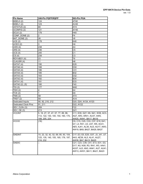
<strong>Pin</strong> Name 240-<strong>Pin</strong> PQFP/RQFP 503-<strong>Pin</strong> PGA<br />
MSEL0 (2) 124 AT40<br />
MSEL1 (2) 123 AV40<br />
nSTATUS (2) 60 AY4<br />
nCONFIG (2) 121 AY40<br />
DCLK (2) 179 H40<br />
CONF_DONE (2) 2 F4<br />
INIT_DONE (3) 26 V6<br />
nCE (2) 178 K40<br />
nCEO (2) 3 H4<br />
nWS (4) 238 A3<br />
nRS (4) 236 C5<br />
nCS (4) 240 C1<br />
CS (4) 239 C3<br />
RDYnBSY (4) 23 T6<br />
CLKUSR (4) 11 H6<br />
DATA7 (4) 190 E29<br />
DATA6 (4) 188 D30<br />
DATA5 (4) 186 C31<br />
DATA4 (4) 185 B32<br />
DATA3 (4) 183 D32<br />
DATA2 (4) 182 B34<br />
DATA1 (4) 181 E33<br />
DATA0 (2), (5) 180 F40<br />
TDI (2) 177 M40<br />
TDO (2) 4 K4<br />
TCK (2) 1 D4<br />
TMS (2) 58 AT4<br />
TRST (2) 59 AV4<br />
Dedicated Inputs 90, 92, 210, 212 D20, D24, AY24, AY20<br />
Dedicated Clock <strong>Pin</strong>s 91, 211 D22, AY22<br />
DEV_CLRn (3) 209 F22<br />
DEV_OE (3) 213 G21<br />
VCCINT 5, 16, 27, 37, 47, 57, 77, 89, 96,<br />
112, 122, 130, 140, 150, 160, 170,<br />
189, 205, 224<br />
C11, E39, G27, N5, N41, W39, AC3,<br />
AG7, AR3, AR41, AU37, AW5,<br />
AW25, AW41, BA17, BA19<br />
VCCIO (16) C9, C15, C25, C33, C37, E19, E41,<br />
G7, L3, R41, U3, U37, W5, AC41,<br />
AE5, AJ41, AL39, AU3, AU17, AW3,<br />
AW19, BA9, BA27, BA29, BA37<br />
GNDINT 10, 22, 32, 42, 52, 69, 85, 93, 104,<br />
125, 135, 145, 155, 165, 176, 197,<br />
216, 232<br />
C17, E3, E5, E25, G37, J3, J41, U7,<br />
AA3, AE39, AL5, AL41, AU27,<br />
AW39, BA7, BA13, BA25<br />
GNDIO – C21, C23, C39, C41, E13, E31, G3,<br />
G17, N3, N39, R3, W41, W3, AA41,<br />
AG37, AJ3, AN3, AN41, AU7, AU41,<br />
AW13, AW31, BA11, BA21, BA23<br />
EPF10K70 Device <strong>Pin</strong>-<strong>Outs</strong><br />
ver. 1.0<br />
<strong>Altera</strong> Corporation 1
<strong>Pin</strong> Name 240-<strong>Pin</strong> PQFP/RQFP 503-<strong>Pin</strong> PGA<br />
No Connect (N.C.) – A19, A21, A23, A31, A33, A35, A39,<br />
A41, B16, B18, B22, B24, B30, B40,<br />
C29, C35, D18, D26, D28, D38, E27,<br />
E37, F18, F2, F26, F30, F32, G23,<br />
G25, G29, G31, G33, G35, K6, K42,<br />
L39, L43, M2, N7, P38, P4, P42,<br />
R37, T40, V42, AC5, AD2, AE3 (11)<br />
Total User I/O <strong>Pin</strong>s (8) 189 358<br />
EPF10K70 Device <strong>Pin</strong>-<strong>Outs</strong><br />
ver. 1.0<br />
<strong>Altera</strong> Corporation 2
Notes:<br />
(1) All pins that are not listed are user I/O pins.<br />
(2) This pin is a dedicated pin; it is not available as a user I/O pin.<br />
(3) This pin can be used as a user I/O pin if it is not used for its device-wide or configuration<br />
function.<br />
(4) This pin can be used as a user I/O pin after configuration.<br />
(5) This pin is tri-stated in user mode.<br />
(6) The optional JTAG pin TRST is not used in the 100-pin or 144-pin TQFP package.<br />
(7) To maintain pin compatibility when transferring to the EPF10K10 or EPF10K10A device from any<br />
other device in the 208-pin PQFP or 256-pin FineLine BGA package, do not use these pins as<br />
user I/O pins.<br />
(8) The user I/O pin count includes dedicated input pins, dedicated clock pins, and all I/O pins.<br />
(9) To maintain pin compatibility when transferring to the EPF10K30 device from any other device in<br />
the 356-pin BGA or 484-pin FineLine BGA package, do not use these pins as user I/O pins.<br />
(10) To maintain pin compatibility when transferring to the EPF10K50V device from any other device<br />
in the 484-pin FineLine BGA package, do not use these pins as user I/O pins.<br />
(11) To maintain pin compatibility when transferring from the EPF10K100 to the EPF10K70 in the 503pin<br />
PGA package, do not use these pins as user I/O pins.<br />
(12) This pin shows the status of the ClockLock and ClockBoost circuitry. When the ClockLock and<br />
ClockBoost circuitry are locked to the incoming clock and generate an internal clock, LOCK is<br />
driven high. LOCK remains high if a periodic clock stops clocking. The LOCK function is optional;<br />
if the LOCK output is not used, this pin is a user I/O pin.<br />
(13) This pin drives the ClockLock and ClockBoost circuitry.<br />
(14) This pin is the power or ground for the ClockLock and ClockBoost circuitry. To ensure noise<br />
resistance, the power and ground supply to the ClockLock and ClockBoost circuitry should be<br />
isolated from the power and ground to the rest of the device.<br />
(15) To maintain pin compatibility when transferring to the EPF10K100A device from another device<br />
in the 600-pin BGA package, do not use these pins as user I/O pins.<br />
(16) The 240-pin QFP packages do not support the MultiVolt I/O feature so there are no VCCIO pins.<br />
EPF10K70 Device <strong>Pin</strong>-<strong>Outs</strong><br />
ver. 1.0<br />
<strong>Altera</strong> Corporation 3
Copyright © 1995, 1996, 1997, 1998, 1999, 2000, 2001 <strong>Altera</strong> Corporation,<br />
101 Innovation Drive, San Jose, CA 95134, USA, all rights reserved.<br />
By accessing this information, you agree to be bound by the terms of <strong>Altera</strong>’s Legal Notice.<br />
13<br />
Development<br />
Tools


