

Functional Description -- HPC II Controller, External Memory ... - Altera
Functional Description -- HPC II Controller, External Memory ... - Altera
Functional Description -- HPC II Controller, External Memory ... - Altera

You also want an ePaper? Increase the reach of your titles
YUMPU automatically turns print PDFs into web optimized ePapers that Google loves.
<strong>Functional</strong> <strong>Description</strong>—<strong>HPC</strong> <strong>II</strong> <strong>Controller</strong><br />
5<br />
2013.12.16<br />
emi_rm_004 Subscribe Send Feedback<br />
The High Performance <strong>Controller</strong> <strong>II</strong> works with the UniPHY-based DDR2, DDR3, and LPDDR2 interfaces.<br />
The controller provides high memory bandwidth, high clock rate performance, and run-time programmability.<br />
The controller can reorder data to reduce row conflicts and bus turn-around time by grouping reads and<br />
writes together, allowing for efficient traffic patterns and reduced latency.<br />
Note: The controller described here is the High Performance <strong>Controller</strong> <strong>II</strong> (<strong>HPC</strong> <strong>II</strong>) with advanced features<br />
for designs generated in the Quartus <strong>II</strong> software version 11.0 and later. Designs created in earlier<br />
versions and regenerated in version 11.0 and later do not inherit the new advanced features; for<br />
information on <strong>HPC</strong> <strong>II</strong> without the version 11.0 and later advanced features, refer to the <strong>External</strong><br />
<strong>Memory</strong> Interface Handbook for Quartus <strong>II</strong> version 10.1, available in the <strong>External</strong> <strong>Memory</strong> Interfaces<br />
section of the <strong>Altera</strong> Literature website.<br />
Related Information<br />
<strong>External</strong> <strong>Memory</strong> Interface Handbook, v10.1<br />
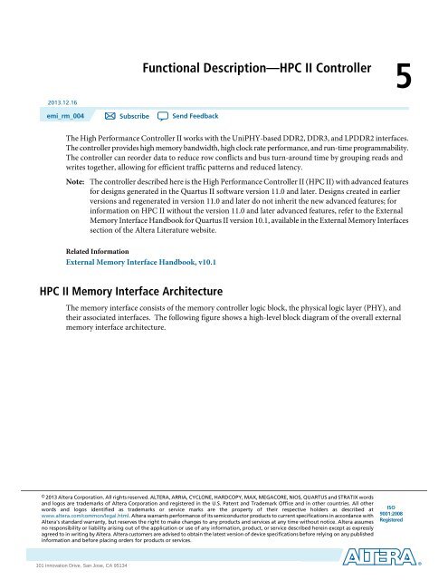
<strong>HPC</strong> <strong>II</strong> <strong>Memory</strong> Interface Architecture<br />
The memory interface consists of the memory controller logic block, the physical logic layer (PHY), and<br />
their associated interfaces. The following figure shows a high-level block diagram of the overall external<br />
memory interface architecture.<br />
© 2013 <strong>Altera</strong> Corporation. All rights reserved. ALTERA, ARRIA, CYCLONE, HARDCOPY, MAX, MEGACORE, NIOS, QUARTUS and STRATIX words<br />
and logos are trademarks of <strong>Altera</strong> Corporation and registered in the U.S. Patent and Trademark Office and in other countries. All other<br />
words and logos identified as trademarks or service marks are the property of their respective holders as described at<br />
www.altera.com/common/legal.html. <strong>Altera</strong> warrants performance of its semiconductor products to current specifications in accordance with<br />
<strong>Altera</strong>'s standard warranty, but reserves the right to make changes to any products and services at any time without notice. <strong>Altera</strong> assumes<br />
no responsibility or liability arising out of the application or use of any information, product, or service described herein except as expressly<br />
agreed to in writing by <strong>Altera</strong>. <strong>Altera</strong> customers are advised to obtain the latest version of device specifications before relying on any published<br />
information and before placing orders for products or services.<br />
ISO<br />
9001:2008<br />
Registered<br />
www.altera.com<br />
101 Innovation Drive, San Jose, CA 95134
5-2<br />
<strong>HPC</strong> <strong>II</strong> <strong>Memory</strong> <strong>Controller</strong> Architecture<br />
Figure 5-1: High-Level Diagram of <strong>Memory</strong> Interface Architecture<br />
emi_rm_004<br />
2013.12.16<br />
<strong>Memory</strong> Interface IP<br />
<strong>Memory</strong> <strong>Controller</strong><br />
PHY<br />
Data Master<br />
Avalon-MM or AXI Converter<br />
Avalon-ST Interface<br />
AFI Interface<br />
AFI Interface<br />
<strong>External</strong> <strong>Memory</strong><br />
CSR Interface<br />
CSR Master<br />
<strong>HPC</strong> <strong>II</strong> <strong>Memory</strong> <strong>Controller</strong> Architecture<br />
The memory controller logic block uses an Avalon Streaming (Avalon-ST) interface as its native interface,<br />
and communicates with the PHY layer by the <strong>Altera</strong> PHY Interface (AFI).<br />
The following figure shows a block diagram of the memory controller architecture.<br />
<strong>Altera</strong> Corporation<br />
<strong>Functional</strong> <strong>Description</strong>—<strong>HPC</strong> <strong>II</strong> <strong>Controller</strong><br />
Send Feedback
emi_rm_004<br />
2013.12.16<br />
Figure 5-2: <strong>Memory</strong> <strong>Controller</strong> Architecture Block Diagram<br />
<strong>HPC</strong> <strong>II</strong> <strong>Memory</strong> <strong>Controller</strong> Architecture<br />
5-3<br />
<strong>Memory</strong> <strong>Controller</strong><br />
Rank Timer<br />
Avalon-ST Input Interface<br />
Command<br />
Generator<br />
Write Data Buffer<br />
Timing Bank<br />
Pool<br />
Arbiter<br />
ECC<br />
AFI Interface to PHY<br />
Read Data Buffer<br />
CSR Interface<br />
Avalon-ST Input Interface<br />
The Avalon-ST interface serves as the entry point to the memory controller, and provides communication<br />
with the requesting data masters.<br />
For information about the Avalon interface, refer to Avalon Interface Specifications.<br />
AXI to Avalon-ST Converter<br />
The <strong>HPC</strong> <strong>II</strong> memory controller includes an AXI to Avalon-ST converter for communication with the AXI<br />
protocol. The AXI to Avalon-ST converter provides write address, write data, write response, read address,<br />
and read data channels on the AXI interface side, and command, write data, and read data channels on the<br />
Avalon-ST interface side.<br />
Handshaking<br />
The AXI protocol employs a handshaking process similar to the Avalon-ST protocol, based on ready and<br />
valid signals.<br />
Command Channel Implementation<br />
<strong>Functional</strong> <strong>Description</strong>—<strong>HPC</strong> <strong>II</strong> <strong>Controller</strong><br />
<strong>Altera</strong> Corporation<br />
Send Feedback
5-4<br />
Backpressure Support<br />
The AXI interface includes separate read and write channels, while the Avalon-ST interface has only one<br />
command channel. Arbitration of the read and write channels is based on these policies:<br />
• Round robin<br />
• Write priority—write channel has priority over read channel<br />
• Read priority—read channel has priority over write channel<br />
You can choose an arbitration policy by setting the COMMAND_ARB_TYPE parameter to one of<br />
ROUND_ROBIN, WRITE_PRIORITY, or READ_PRIORITY in the alt_mem_ddrx_axi_st_converter.v file.<br />
Data Ordering<br />
The AXI specification requires that write data IDs must arrive in the same order as write address IDs are<br />
received. Similarly, read data must be returned in the same order as its associated read address is received.<br />
Consequently, the AXI to Avalon-ST converter does not support interleaving of write data; all data must<br />
arrive in the same order as its associated write address IDs. On the read side, the controller returns read data<br />
based on the read addresses received.<br />
Burst Types<br />
The AXI to Avalon-ST converter supports the following burst types:<br />
emi_rm_004<br />
2013.12.16<br />
• Incrementing burst—the address for each transfer is an increment of the previous transfer address; the<br />
increment value depends on the size of the transfer.<br />
• Wrapping burst—similar to the incrementing burst, but wraps to the lower address when the burst<br />
boundary is reached. The starting address must be aligned to the size of the transfer. Burst length must<br />
be 2, 4, 8, or 16. The burst wrap boundary = burst size * burst length.<br />
Related Information<br />
Avalon Interface Specifications<br />
Backpressure Support<br />
The write response and read data channels do not support data transfer with backpressure; consequently,<br />
you must assert the ready signal for the write response and read data channels to 1 to ensure acceptance of<br />
data at any time.<br />
Figure 5-3: Data Transfer Without Backpressure<br />
clk<br />
rready<br />
rvalid<br />
rid<br />
rresp<br />
rdata D0 D1 D2 D3<br />
For information about data transfer with and without backpressure, refer to the Avalon Interface Specifications.<br />
Related Information<br />
Avalon Interface Specifications<br />
<strong>Altera</strong> Corporation<br />
<strong>Functional</strong> <strong>Description</strong>—<strong>HPC</strong> <strong>II</strong> <strong>Controller</strong><br />
Send Feedback
emi_rm_004<br />
2013.12.16<br />
Command Generator<br />
The command generator accepts commands from the front-end Avalon-ST interface and from local ECC<br />
internal logic, and provides those commands to the timing bank pool.<br />
Timing Bank Pool<br />
The timing bank pool is a parallel queue that works with the arbiter to enable data reordering. The timing<br />
bank pool tracks incoming requests, ensures that all timing requirements are met and, upon receiving<br />
write-data-ready notification from the write data buffer, passes the requests to the arbiter in an ordered and<br />
efficient manner.<br />
Arbiter<br />
The arbiter determines the order in which requests are passed to the memory device. When the arbiter<br />
receives a single request, that request is passed immediately; however, when multiple requests are received,<br />
the arbiter uses arbitration rules to determine the order in which to pass requests to the memory device.<br />
Arbitration Rules<br />
The arbiter uses the following arbitration rules:<br />
• If only one master is issuing a request, grant that request immediately.<br />
• If there are outstanding requests from two or more masters, the arbiter applies the following tests, in<br />
order:<br />
• Is there a read request? If so, the arbiter grants the read request ahead of any write requests.<br />
• If neither of the above conditions apply, the arbiter grants the oldest request first.<br />
Rank Timer<br />
The rank timer maintains rank-specific timing information, and performs the following functions:<br />
• Ensures that only four activates occur within a specified timing window.<br />
• Manages the read-to-write and write-to-read bus turnaround time.<br />
• Manages the time-to-activate delay between different banks.<br />
Read Data Buffer and Write Data Buffer<br />
The read data buffer receives data from the PHY and passes that data through the input interface to the<br />
master. The write data buffer receives write data from the input interface and passes that data to the PHY,<br />
upon approval of the write request.<br />
ECC Block<br />
The error-correcting code (ECC) block comprises an encoder and a decoder-corrector, which can detect<br />
and correct single-bit errors, and detect double-bit errors. The ECC block can remedy errors resulting from<br />
noise or other impairments during data transmission.<br />
AFI and CSR Interfaces<br />
The AFI interface provides communication between the controller and the physical layer logic (PHY). The<br />
CSR interface provides communication with your system’s internal control status registers.<br />
For more information about AFI signals, refer to AFI 3.0 Specification in the <strong>Functional</strong> <strong>Description</strong> - UniPHY<br />
chapter.<br />
Note:<br />
Unaligned reads and writes on the AFI interface are not supported.<br />
Command Generator<br />
5-5<br />
<strong>Functional</strong> <strong>Description</strong>—<strong>HPC</strong> <strong>II</strong> <strong>Controller</strong><br />
<strong>Altera</strong> Corporation<br />
Send Feedback
5-6<br />
<strong>HPC</strong> <strong>II</strong> <strong>Controller</strong> Features<br />
Related Information<br />
• Avalon Interface Specifications<br />
• <strong>Functional</strong> <strong>Description</strong> - UniPHY<br />
emi_rm_004<br />
2013.12.16<br />
<strong>HPC</strong> <strong>II</strong> <strong>Controller</strong> Features<br />
The <strong>HPC</strong> <strong>II</strong> memory controller offers a variety of features.<br />
Data Reordering<br />
The controller implements data reordering to maximize efficiency for read and write commands. The<br />
controller can reorder read and write commands as necessary to mitigate bus turn-around time and reduce<br />
conflict between rows.<br />
Inter-bank data reordering reorders commands going to different bank addresses. Commands going to the<br />
same bank address are not reordered. This reordering method implements simple hazard detection on the<br />
bank address level.<br />
The controller implements logic to limit the length of time that a command can go unserved. This logic is<br />
known as starvation control. In starvation control, a counter is incremented for every command served. You<br />
can set a starvation limit, to ensure that a waiting command is served immediately, when the starvation<br />
counter reaches the specified limit.<br />
Pre-emptive Bank Management<br />
Data reordering allows the controller to issue bank-management commands pre-emptively, based on the<br />
patterns of incoming commands. The desired page in memory can be already open when a command reaches<br />
the AFI interface.<br />
Quasi-1T and Quasi-2T<br />
One controller clock cycle equals two memory clock cycles in a half-rate interface, and to four memory clock<br />
cycles in a quarter-rate interface. To fully utilize the command bandwidth, the controller can operate in<br />
Quasi-1T half-rate and Quasi-2T quarter-rate modes.<br />
In Quasi-1T and Quasi-2T modes, the controller issues two commands on every controller clock cycle. The<br />
controller is constrained to issue a row command on the first clock phase and a column command on the<br />
second clock phase, or vice versa. Row commands include activate and precharge commands; column<br />
commands include read and write commands.<br />
The controller operates in Quasi-1T in half-rate mode, and in Quasi-2T in quarter-rate mode; this operation<br />
is transparent and has no user settings.<br />
User Autoprecharge Commands<br />
The autoprecharge read and autoprecharge write commands allow you to indicate to the memory device<br />
that this read or write command is the last access to the currently open row. The memory device automatically<br />
closes or autoprecharges the page it is currently accessing so that the next access to the same bank is quicker.<br />
This command is useful for applications that require fast random accesses.<br />
Since the <strong>HPC</strong> <strong>II</strong> controller can reorder transactions for best efficiency, when you assert the<br />
local_autopch_req signal, the controller evaluates the current command and buffered commands to<br />
determine the best autoprecharge operation.<br />
<strong>Altera</strong> Corporation<br />
<strong>Functional</strong> <strong>Description</strong>—<strong>HPC</strong> <strong>II</strong> <strong>Controller</strong><br />
Send Feedback
emi_rm_004<br />
2013.12.16<br />
Address and Command Decoding Logic<br />
When the main state machine issues a command to the memory, it asserts a set of internal signals. The<br />
address and command decoding logic turns these signals into AFI-specific commands and address.<br />
The following signals are generated:<br />
• Clock enable and reset signals: afi_cke, afi_rst_n<br />
• Command and address signals: afi_cs_n, afi_ba, afi_addr, afi_ras_n, afi_cas_n,<br />
afi_we_n<br />
Low-Power Logic<br />
There are two types of low-power logic: the user-controlled self-refresh logic and automatic power-down<br />
with programmable time-out logic.<br />
User-Controlled Self-Refresh<br />
When you assert the local_self_rfsh_req signal, the controller completes any currently executing<br />
reads and writes, and then interrupts the command queue and immediately places the memory into selfrefresh<br />
mode. When the controller places the memory into self-refresh mode, it responds by asserting an<br />
acknowledge signal, local_self_rfsh_ack. You can leave the memory in self-refresh mode for as<br />
long as you choose.<br />
To bring the memory out of self-refresh mode, you must deassert the request signal, and the controller<br />
responds by deasserting the acknowledge signal when the memory is no longer in self-refresh mode.<br />
Note:<br />
Address and Command Decoding Logic<br />
If a user-controlled refresh request and a system-generated refresh request occur at the same time,<br />
the user-controlled refresh takes priority; the system-generated refresh is processed only after the<br />
user-controlled refresh request is completed.<br />
5-7<br />
Automatic Power-Down with Programmable Time-Out<br />
The controller automatically places the memory in power-down mode to save power if the requested number<br />
of idle controller clock cycles is observed in the controller. The Auto Power Down Cycles parameter on<br />
the <strong>Controller</strong> Settings tab allows you to specify a range between 1 to 65,535 idle controller clock cycles.<br />
The counter for the programmable time-out starts when there are no user read or write requests in the<br />
command queue. Once the controller places the memory in power-down mode, it responds by asserting the<br />
acknowledge signal, local_power_down_ack.<br />
ODT Generation Logic<br />
The on-die termination (ODT) generation logic generates the necessary ODT signals for the controller,<br />
based on the scheme that <strong>Altera</strong> recommends.<br />
DDR2 SDRAM<br />
Note:<br />
There is no ODT for reads.<br />
Table 5-1: ODT—DDR2 SDRAM Single Slot Single Chip-select Per DIMM (Write)<br />
Write On<br />
ODT Enabled<br />
mem_cs[0]<br />
mem_odt [0]<br />
<strong>Functional</strong> <strong>Description</strong>—<strong>HPC</strong> <strong>II</strong> <strong>Controller</strong><br />
<strong>Altera</strong> Corporation<br />
Send Feedback
5-8<br />
ODT Generation Logic<br />
Note:<br />
There is no ODT for reads.<br />
emi_rm_004<br />
2013.12.16<br />
Table 5-2: ODT—DDR2 SDRAM Single Slot Dual Chip-select Per DIMM (Write)<br />
Write On<br />
ODT Enabled<br />
mem_cs[0]<br />
mem_odt [0]<br />
mem_cs[1]<br />
mem_odt[1]<br />
Table 5-3: ODT—DDR2 SDRAM Dual Slot Single Chip-select Per DIMM (Write)<br />
Write On<br />
ODT Enabled<br />
mem_cs[0]<br />
mem_odt [1]<br />
mem_cs[1]<br />
mem_odt[0]<br />
Table 5-4: ODT—DDR2 SDRAM Dual Slot Dual Chip-select Per DIMM (Write)<br />
Write On<br />
ODT Enabled<br />
mem_cs[0]<br />
mem_odt[2]<br />
mem_cs[1]<br />
mem_odt[3]<br />
mem_cs[2]<br />
mem_odt[0]<br />
mem_cs[3]<br />
mem_odt[1]<br />
DDR3 SDRAM<br />
Note: There is no ODT for reads.<br />
Table 5-5: ODT—DDR3 SDRAM Single Slot Single Chip-select Per DIMM (Write)<br />
Write On<br />
ODT Enabled<br />
mem_cs[0]<br />
mem_odt [0]<br />
Note:<br />
There is no ODT for reads.<br />
<strong>Altera</strong> Corporation<br />
<strong>Functional</strong> <strong>Description</strong>—<strong>HPC</strong> <strong>II</strong> <strong>Controller</strong><br />
Send Feedback
emi_rm_004<br />
2013.12.16<br />
Table 5-6: ODT—DDR3 SDRAM Single Slot Dual Chip-select Per DIMM (Write)<br />
ODT Generation Logic<br />
5-9<br />
Write On<br />
ODT Enabled<br />
mem_cs[0]<br />
mem_odt [0]<br />
mem_cs[1]<br />
mem_odt[1]<br />
Table 5-7: ODT—DDR3 SDRAM Dual Slot Single Chip-select Per DIMM (Write)<br />
Write On<br />
ODT Enabled<br />
mem_cs[0]<br />
mem_cs[1]<br />
mem_odt [0] and mem_odt [1]<br />
mem_odt [0] and mem_odt [1]<br />
Table 5-8: ODT—DDR3 SDRAM Dual Slot Single Chip-select Per DIMM (Read)<br />
Read On<br />
ODT Enabled<br />
mem_cs[0]<br />
mem_odt[1]<br />
mem_cs[1]<br />
mem_odt[0]<br />
Table 5-9: ODT—DDR3 SDRAM Dual Slot Dual Chip-select Per DIMM (Write)<br />
Write On<br />
ODT Enabled<br />
mem_cs[0]<br />
mem_cs[1]<br />
mem_cs[2]<br />
mem_cs[3]<br />
mem_odt [0] and mem_odt [2]<br />
mem_odt [1]and mem_odt [3]<br />
mem_odt [0]and mem_odt [2]<br />
mem_odt [1]and mem_odt [3]<br />
<strong>Functional</strong> <strong>Description</strong>—<strong>HPC</strong> <strong>II</strong> <strong>Controller</strong><br />
<strong>Altera</strong> Corporation<br />
Send Feedback
5-10<br />
Burst Merging<br />
Table 5-10: ODT—DDR3 SDRAM Dual Slot Dual Rank Per DIMM (Read)<br />
emi_rm_004<br />
2013.12.16<br />
Read On<br />
ODT Enabled<br />
mem_cs[0]<br />
mem_odt[2]<br />
mem_cs[1]<br />
mem_odt[3]<br />
mem_cs[2]<br />
mem_odt[0]<br />
mem_cs[3]<br />
mem_odt[1]<br />
Burst Merging<br />
The burst merging feature improves controller efficiency by merging two burst chop commands of sequential<br />
addresses into one burst length command.<br />
Burst merging is opportunistic and happens when the controller receives commands faster than it can process<br />
(for example, Avalon commands of multiple burst length) or when the controller temporarily stops processing<br />
commands due to Refresh.<br />
The burst merging feature is turned off by default when you generate a controller. If your traffic exercises<br />
patterns that you can merge, you should turn on burst merging, as follows:<br />
1. In a text editor, open the _c0.v top-level file for your design.<br />
2. Search for the ENABLE_BURST_MERGE parameter in the .v file.<br />
3. Change the ENABLE_BURST_MERGE value from 0 to 1.<br />
ECC<br />
The ECC logic comprises an encoder and a decoder-corrector, which can detect and correct single-bit errors,<br />
and detect double-bit errors. The ECC logic is available in multiples of 16, 24, 40, and 72 bits.<br />
Note:<br />
For the hard memory controller with multiport front end available in Arria V and Cyclone V devices,<br />
ECC logic is limited to widths of 24 and 40.<br />
• The ECC logic has the following features:<br />
• Has Hamming code ECC logic that encodes every 64, 32, 16, or 8 bits of data into 72, 40, 24, or 16 bits<br />
of codeword.<br />
• Has a latency increase of one clock for both writes and reads.<br />
• For a 128-bit interface, ECC is generated as one 64-bit data path with 8-bits of ECC path, plus a second<br />
64-bit data path with 8-bits of ECC path.<br />
• Detects and corrects all single-bit errors.<br />
• Detects all double-bit errors.<br />
• Counts the number of single-bit and double-bit errors.<br />
• Accepts partial writes, which trigger a read-modify-write cycle, for memory devices with DM pins.<br />
• Can inject single-bit and double-bit errors to trigger ECC correction for testing and debugging purposes.<br />
• Generates an interrupt signal when an error occurs.<br />
<strong>Altera</strong> Corporation<br />
<strong>Functional</strong> <strong>Description</strong>—<strong>HPC</strong> <strong>II</strong> <strong>Controller</strong><br />
Send Feedback
emi_rm_004<br />
2013.12.16<br />
Note:<br />
Partial Writes<br />
When using ECC, you must initialize your entire memory content to zero before beginning to write<br />
to the memory. If you do not initialize the content to zero, and if you read from uninitialized memory<br />
locations without having first written to them, you will see junk data which will trigger an ECC<br />
interrupt.<br />
5-11<br />
When a single-bit or double-bit error occurs, the ECC logic triggers the ecc_interrupt signal to inform<br />
you that an ECC error has occurred. When a single-bit error occurs, the ECC logic reads the error address,<br />
and writes back the corrected data. When a double-bit error occurs, the ECC logic does not do any error<br />
correction but it asserts the avl_rdata_error signal to indicate that the data is incorrect. The<br />
avl_rdata_error signal follows the same timing as the avl_rdata_valid signal.<br />
Enabling autocorrection allows the ECC logic to delay all controller pending activities until the correction<br />
completes. You can disable autocorrection and schedule the correction manually when the controller is idle<br />
to ensure better system efficiency. To manually correct ECC errors, follow these steps:<br />
1. When an interrupt occurs, read out the SBE_ERROR register. When a single-bit error occurs, the<br />
SBE_ERROR register is equal to one.<br />
2. Read out the ERR_ADDR register.<br />
3. Correct the single-bit error by issuing a dummy write to the memory address stored in the ERR_ADDR<br />
register. A dummy write is a write request with the local_be signal zero, that triggers a partial write<br />
which is effectively a read-modify-write event. The partial write corrects the data at that address and<br />
writes it back.<br />
Partial Writes<br />
The ECC logic supports partial writes.<br />
Along with the address, data, and burst signals, the Avalon-MM interface also supports a signal vector,<br />
local_be, that is responsible for byte-enable. Every bit of this signal vector represents a byte on the databus.<br />
Thus, a logic low on any of these bits instructs the controller not to write to that particular byte, resulting<br />
in a partial write. The ECC code is calculated on all bytes of the data-bus. If any bytes are changed, the IP<br />
core must recalculate the ECC code and write the new code back to the memory.<br />
For partial writes, the ECC logic performs the following steps:<br />
1. The ECC logic sends a read command to the partial write address.<br />
2. Upon receiving a return data from the memory for the particular address, the ECC logic decodes the<br />
data, checks for errors, and then merges the corrected or correct dataword with the incoming information.<br />
3. The ECC logic issues a write to write back the updated data and the new ECC code.<br />
The following corner cases can occur:<br />
• A single-bit error during the read phase of the read-modify-write process. In this case, the IP core corrects<br />
the single-bit error first, increments the single-bit error counter and then performs a partial write to this<br />
corrected decoded data word.<br />
• A double-bit error during the read phase of the read-modify-write process. In this case, the IP core<br />
increments the double-bit error counter and issues an interrupt. The IP core writes a new write word to<br />
the location of the error. The ECC status register keeps track of the error information.<br />
The following figures show partial write operations for the controller, for full and half rate configurations,<br />
respectively.<br />
<strong>Functional</strong> <strong>Description</strong>—<strong>HPC</strong> <strong>II</strong> <strong>Controller</strong><br />
<strong>Altera</strong> Corporation<br />
Send Feedback
5-12<br />
Partial Bursts<br />
Figure 5-4: Partial Write for the <strong>Controller</strong>--Full Rate<br />
emi_rm_004<br />
2013.12.16<br />
avl_address<br />
avl_size<br />
avl_be<br />
avl_wdata<br />
mem_dm<br />
mem_dq<br />
0 1<br />
2<br />
X1 XF<br />
01234567 89ABCDEF<br />
67 R R R EF CD AB 89<br />
Figure 5-5: Partial Write for the <strong>Controller</strong>--Half Rate<br />
avl_address<br />
avl_size<br />
avl_be<br />
avl_wdata<br />
mem_dm<br />
mem_dq<br />
0<br />
1<br />
X1<br />
01234567<br />
67 R R R<br />
Partial Bursts<br />
DIMMs that do not have the DM pins do not support partial bursts. You must write a minimum (or<br />
multiples) of memory-burst-length-equivalent words to the memory at the same time.<br />
The following figure shows a partial burst operation for the controller.<br />
Figure 5-6: Partial Burst for <strong>Controller</strong><br />
avl_address<br />
avl_size<br />
avl_be<br />
avl_wdata<br />
mem_dm<br />
mem_dq<br />
0<br />
1<br />
X1<br />
01234567<br />
67 45 23 01<br />
<strong>External</strong> Interfaces<br />
This section discusses the interfaces between the controller and other external memory interface components.<br />
<strong>Altera</strong> Corporation<br />
<strong>Functional</strong> <strong>Description</strong>—<strong>HPC</strong> <strong>II</strong> <strong>Controller</strong><br />
Send Feedback
emi_rm_004<br />
2013.12.16<br />
Clock and Reset Interface<br />
The clock and reset interface is part of the AFI interface.<br />
The controller can have up to two clock domains, which are synchronous to each other. The controller<br />
operates with a single clock domain when there is no integrated half-rate bridge, and with two-clock domains<br />
when there is an integrated half-rate bridge. The clocks are provided by UniPHY.<br />
The main controller clock is afi_clk, and the optional half-rate controller clock is afi_half_clk. The<br />
main and half-rate clocks must be synchronous and have a 2:1 frequency ratio. The optional quarter-rate<br />
controller clock is afi_quarter_clk, which must also be synchronous and have a 4:1 frequency ratio.<br />
Avalon-ST Data Slave Interface<br />
The Avalon-ST data slave interface consists of the following Avalon-ST channels, which together form a<br />
single data slave:<br />
• The command channel, which serves as command and address for both read and write operations.<br />
• The write data channel, which carries write data.<br />
• The read data channel, which carries read data.<br />
For information about the Avalon interface, refer to Avalon Interface Specifications.<br />
AXI Data Slave Interface<br />
The AXI data interface consists of the following channels, which communicate with the Avalon-ST interface<br />
through the AXI to Avalon-ST converter:<br />
• The write address channel, which carries address information for write operations.<br />
• The write data channel, which carries write data.<br />
• The write response channel, which carries write response data.<br />
• The read address channel, which carries address information for read operations.<br />
• The read data channel, which carries read data.<br />
Related Information<br />
Avalon Interface Specifications<br />
<strong>Controller</strong>-PHY Interface<br />
The interface between the controller and the PHY is part of the AFI interface. The controller assumes that<br />
the PHY performs all necessary calibration processes without any interaction with the controller.<br />
For more information about AFI signals, refer to AFI 3.0 Specification.<br />
<strong>Memory</strong> Side-Band Signals<br />
The <strong>HPC</strong> <strong>II</strong> controller supports several optional side-band signals.<br />
Self-Refresh (Low Power) Interface<br />
<strong>Controller</strong>-PHY Interface<br />
The optional low power self-refresh interface consists of a request signal and an acknowledgement signal,<br />
which you can use to instruct the controller to place the memory device into self-refresh mode. This interface<br />
is clocked by afi_clk.<br />
When you assert the request signal, the controller places the memory device into self-refresh mode and<br />
asserts the acknowledge signal. To bring the memory device out of self-refresh mode, you deassert the request<br />
5-13<br />
<strong>Functional</strong> <strong>Description</strong>—<strong>HPC</strong> <strong>II</strong> <strong>Controller</strong><br />
<strong>Altera</strong> Corporation<br />
Send Feedback
5-14<br />
<strong>Controller</strong> <strong>External</strong> Interfaces<br />
emi_rm_004<br />
2013.12.16<br />
signal; the controller then deasserts the acknowledge signal when the memory device is no longer in selfrefresh<br />
mode.<br />
Note: For multi-rank designs using the <strong>HPC</strong> <strong>II</strong> memory controller, a self-refresh and a user-refresh cannot<br />
be made to the same memory chip simultaneously. Also, the self-refresh ack signal indicates that<br />
at least one device has entered self-refresh, but does not necessarily mean that all devices have entered<br />
self-refresh.<br />
User-Controlled Refresh Interface<br />
The optional user-controlled refresh interface consists of a request signal, a chip select signal, and an<br />
acknowledgement signal. This interface provides increased control over worst-case read latency and enables<br />
you to issue refresh bursts during idle periods. This interface is clocked by afi_clk.<br />
When you assert a refresh request signal to instruct the controller to perform a refresh operation, that request<br />
takes priority over any outstanding read or write requests that might be in the command queue. In addition<br />
to the request signal, you must also choose the chip to be refreshed by asserting the refresh chip select signal<br />
along with the request signal. If you do not assert the chip select signal with the request signal, unexpected<br />
behavior may result.<br />
The controller attempts to perform a refresh as long as the refresh request signal is asserted; if you require<br />
only one refresh, you should deassert the refresh request signal after the acknowledgement signal is received.<br />
If you maintain the request signal high after the acknowledgement is sent, it would indicate that further<br />
refresh is required. You should deassert the request signal after the required number of acknowledgement/refresh<br />
is received from the controller. You can issue up to a maximum of nine consecutive refresh<br />
commands.<br />
Note:<br />
For multi-rank designs using the <strong>HPC</strong> <strong>II</strong> memory controller, a self-refresh and a user-refresh cannot<br />
be made to the same memory chip simultaneously.<br />
Configuration and Status Register (CSR) Interface<br />
The controller has a configuration and status register (CSR) interface that allows you to configure timing<br />
parameters, address widths, and the behavior of the controller. The CSR interface is a 32-bit Avalon-MM<br />
slave of fixed address width; if you do not need this feature, you can disable it to save area.<br />
This interface is clocked by csr_clk, which is the same as afi_clk, and is always synchronous relative<br />
to the main data slave interface.<br />
<strong>Controller</strong> <strong>External</strong> Interfaces<br />
The following table lists the controller’s external interfaces.<br />
Table 5-11: Summary of <strong>Controller</strong> <strong>External</strong> Interfaces<br />
Interface Name<br />
Display Name<br />
Type<br />
<strong>Description</strong><br />
Clock and Reset Interface<br />
Clock and Reset<br />
Interface<br />
Clock and Reset Interface<br />
AFI (1)<br />
Clock and reset<br />
generated by UniPHY to<br />
the controller.<br />
Avalon-ST Data Slave Interface<br />
<strong>Altera</strong> Corporation<br />
<strong>Functional</strong> <strong>Description</strong>—<strong>HPC</strong> <strong>II</strong> <strong>Controller</strong><br />
Send Feedback
emi_rm_004<br />
2013.12.16<br />
<strong>Controller</strong> <strong>External</strong> Interfaces<br />
5-15<br />
Interface Name<br />
Display Name<br />
Type<br />
<strong>Description</strong><br />
Command Channel<br />
Avalon-ST Data Slave<br />
Interface<br />
Avalon-ST (2)<br />
Address and command<br />
channel for read and<br />
write, single command<br />
single data (SCSD).<br />
Write Data Channel<br />
Avalon-ST Data Slave<br />
Interface<br />
Avalon-ST (2)<br />
Write Data Channel,<br />
single command<br />
multiple data (SCMD).<br />
Read Data Channel<br />
Avalon-ST Data Slave<br />
Interface<br />
Avalon-ST (2)<br />
Read data channel,<br />
SCMD with read data<br />
error response.<br />
<strong>Controller</strong>-PHY Interface<br />
AFI 3.0<br />
AFI Interface<br />
AFI (1)<br />
Interface between<br />
controller and PHY.<br />
<strong>Memory</strong> Side-Band Signals<br />
Self Refresh (Low<br />
Power) Interface<br />
Self Refresh (Low Power)<br />
Interface<br />
Avalon Control & Status<br />
Interface (2)<br />
SDRAM-specific signals<br />
to place memory into<br />
low-power mode.<br />
User-<strong>Controller</strong> Refresh<br />
Interface<br />
User-<strong>Controller</strong> Refresh<br />
Interface<br />
Avalon Control & Status<br />
Interface (2)<br />
SDRAM-specific signals<br />
to request memory<br />
refresh.<br />
Configuration and Status Register (CSR) Interface<br />
CSR<br />
Configuration and Status<br />
Register Interface<br />
Avalon-MM (2)<br />
Enables on-the-fly<br />
configuration of<br />
memory timing<br />
parameters, address<br />
widths, and controller<br />
behaviour.<br />
Notes:<br />
1. For information about AFI signals, refer to AFI 3.0 Specification in the <strong>Functional</strong> <strong>Description</strong> - UniPHY<br />
chapter.<br />
2. For information about Avalon signals, refer to Avalon Interface Specifications.<br />
Related Information<br />
• Avalon Interface Specifications<br />
• <strong>Functional</strong> <strong>Description</strong> - UniPHY<br />
<strong>Functional</strong> <strong>Description</strong>—<strong>HPC</strong> <strong>II</strong> <strong>Controller</strong><br />
<strong>Altera</strong> Corporation<br />
Send Feedback
5-16<br />
Top-Level Signals <strong>Description</strong><br />
emi_rm_004<br />
2013.12.16<br />
Top-Level Signals <strong>Description</strong><br />
The top-level signals include clock and reset signals, local interface signals, controller interface signals, and<br />
CSR interface signals.<br />
Clock and Reset Signals<br />
The following table lists the clock and reset signals.<br />
Note:<br />
The suffix _n denotes active low signals.<br />
<strong>Altera</strong> Corporation<br />
<strong>Functional</strong> <strong>Description</strong>—<strong>HPC</strong> <strong>II</strong> <strong>Controller</strong><br />
Send Feedback
emi_rm_004<br />
2013.12.16<br />
Table 5-12: Clock and Reset Signals<br />
Clock and Reset Signals<br />
5-17<br />
Name<br />
global_reset_n<br />
pll_ref_clk<br />
phy_clk<br />
reset_phy_clk_n<br />
aux_full_rate_clk<br />
aux_half_rate_clk<br />
dll_reference_clk<br />
reset_request_n<br />
Direction<br />
Input<br />
Input<br />
Output<br />
Output<br />
Output<br />
Output<br />
Output<br />
Output<br />
<strong>Description</strong><br />
The asynchronous reset input to the<br />
controller. The IP core derives all other reset<br />
signals from resynchronized versions of this<br />
signal. This signal holds the PHY, including<br />
the PLL, in reset while low.<br />
The reference clock input to PLL.<br />
The system clock that the PHY provides to<br />
the user. All user inputs to and outputs from<br />
the controller must be synchronous to this<br />
clock.<br />
The reset signal that the PHY provides to the<br />
user. The IP core asserts reset_phy_clk_<br />
n asynchronously and deasserts<br />
synchronously to phy_clk clock domain.<br />
An alternative clock that the PHY provides<br />
to the user. This clock always runs at the same<br />
frequency as the external memory interface.<br />
In half-rate designs, this clock is twice the<br />
frequency of the phy_clk and you can use<br />
it whenever you require a 2x clock. In fullrate<br />
designs, the same PLL output as the<br />
phy_clk signal drives this clock.<br />
An alternative clock that the PHY provides<br />
to the user. This clock always runs at half the<br />
frequency as the external memory interface.<br />
In full-rate designs, this clock is half the<br />
frequency of the phy_clk and you can use<br />
it, for example to clock the user side of a halfrate<br />
bridge. In half-rate designs, or if the<br />
Enable Half Rate Bridge option is turned on.<br />
The same PLL output that drives the phy_<br />
clk signal drives this clock.<br />
Reference clock to feed to an externally<br />
instantiated DLL.<br />
Reset request output that indicates when the<br />
PLL outputs are not locked. Use this signal<br />
as a reset request input to any system-level<br />
reset controller you may have. This signal is<br />
always low when the PLL is trying to lock,<br />
and so any reset logic using <strong>Altera</strong> advises<br />
you detect a reset request on a falling edge<br />
rather than by level detection.<br />
<strong>Functional</strong> <strong>Description</strong>—<strong>HPC</strong> <strong>II</strong> <strong>Controller</strong><br />
Send Feedback<br />
<strong>Altera</strong> Corporation
5-18<br />
Local Interface Signals<br />
emi_rm_004<br />
2013.12.16<br />
Name<br />
soft_reset_n<br />
seriesterminationcontrol<br />
parallelterminationcontrol<br />
oct_rdn<br />
oct_rup<br />
dqs_delay_ctrl_import<br />
csr_clk<br />
Direction<br />
Input<br />
Input (for<br />
OCT slave)<br />
Output (for<br />
OCT master)<br />
Input (for<br />
OCT slave)<br />
Output (for<br />
OCT master)<br />
Input (for<br />
OCT master)<br />
Input (for<br />
OCT master)<br />
Input<br />
Output<br />
<strong>Description</strong><br />
Edge detect reset input for control by other<br />
system reset logic. Assert to cause a complete<br />
reset to the PHY, but not to the PLL that the<br />
PHY uses.<br />
Required signal for PHY to provide series<br />
termination calibration value. Must be<br />
connected to a user-instantiated OCT control<br />
block (alt_oct) or another UniPHY instance<br />
that is set to OCT master mode.<br />
Unconnected PHY signal, available for<br />
sharing with another PHY.<br />
Must connect to calibration resistor tied to<br />
GND on the appropriate RDN pin on the<br />
device. (Refer to appropriate device<br />
handbook.)<br />
Must connect to calibration resistor tied to<br />
Vccio on the appropriate RUP pin on the<br />
device. (See appropriate device handbook.)<br />
Allows the use of DLL in another PHY<br />
instance in this PHY instance. Connect the<br />
export port on the PHY instance with a<br />
DLL to the import port on the other PHY<br />
instance.<br />
Clock for the configuration and status register<br />
(CSR) interface, which is the same as afi_<br />
clk and is always synchronous relative to<br />
the main data slave interface.<br />
Note:<br />
1. Applies only to the hard memory controller with multiport front end available in Arria V and Cyclone V<br />
devices.<br />
Local Interface Signals<br />
The following table lists the controller local interface signals.<br />
<strong>Altera</strong> Corporation<br />
<strong>Functional</strong> <strong>Description</strong>—<strong>HPC</strong> <strong>II</strong> <strong>Controller</strong><br />
Send Feedback
emi_rm_004<br />
2013.12.16<br />
Table 5-13: Local Interface Signals<br />
Local Interface Signals<br />
5-19<br />
Signal Name<br />
avl_addr[] (1)<br />
Direction<br />
Input<br />
<strong>Description</strong><br />
<strong>Functional</strong> <strong>Description</strong>—<strong>HPC</strong> <strong>II</strong> <strong>Controller</strong><br />
<strong>Altera</strong> Corporation<br />
Send Feedback
5-20<br />
Local Interface Signals<br />
emi_rm_004<br />
2013.12.16<br />
Signal Name<br />
Direction<br />
<strong>Description</strong><br />
<strong>Memory</strong> address at which the burst should start. By default, the IP<br />
core maps local address to the bank interleaving scheme. You can<br />
change the ordering via the Local-to-<strong>Memory</strong> Address Mapping<br />
option in the <strong>Controller</strong> Settings page.<br />
This signal must remain stable only during the first transaction of a<br />
burst. The constantBurstBehavior property is always false for<br />
UniPHY controllers.<br />
The IP core sizes the width of this bus according to the following<br />
equations:<br />
• Full rate controllers:<br />
For one chip select: width = row bits + bank bits + column bits – 1<br />
For multiple chip selects: width = chip bits* + row bits + bank bits +<br />
column bits – 1<br />
If the bank address is 2 bits wide, row is 13 bits wide and column is 10<br />
bits wide, the local address is 24 bits wide. To map local_address<br />
to bank, row and column address:<br />
avl_addr is 24 bits wide<br />
avl_addr[23:11]= row address[12:0]<br />
avl_addr[10:9] = bank address [1:0]<br />
avl_addr[8:0] = column address[9:1]<br />
The IP core ignores the least significant bit (LSB) of the column address<br />
(multiples of two) on the memory side, because the local data width<br />
is twice that of the memory data bus width.<br />
• Half rate controllers:<br />
For one chip select: width = row bits + bank bits + column bits – 2<br />
For multiple chip selects: width = chip bits* + row bits + bank bits +<br />
column bits – 2<br />
If the bank address is 2 bits wide, row is 13 bits wide and column is 10<br />
bits wide, the local address is 23 bits wide. To map local_address<br />
to bank, row and column address:<br />
avl_addr is 23 bits wide<br />
avl_addr[22:10] = row address[12:0]<br />
avl_addr[9:8] = bank address [1:0]<br />
avl_addr[7:0] = column address[9:2]<br />
The IP core ignores two LSBs of the column address (multiples of four)<br />
on the memory side, because the local data width is four times that of<br />
the memory data bus width.<br />
• Quarter rate controllers:<br />
For one chip select: width = row bits + bank bits + column bits – 3<br />
For multiple chip selects: width = chip bits* + row bits + bank bits +<br />
<strong>Altera</strong> Corporation<br />
<strong>Functional</strong> <strong>Description</strong>—<strong>HPC</strong> <strong>II</strong> <strong>Controller</strong><br />
Send Feedback
emi_rm_004<br />
2013.12.16<br />
Local Interface Signals<br />
5-21<br />
Signal Name<br />
Direction<br />
<strong>Description</strong><br />
column bits – 3<br />
If the bank address is 2 bits wide, row is 13 bits wide and column is 10<br />
bits wide, the local address is 22 bits wide.<br />
(* chip bits is a derived value indicating the number of address bits<br />
necessary to uniquely address every memory rank in the system; this<br />
value is not user configurable.)<br />
avl_be[]<br />
(2)<br />
Input<br />
Byte enable signal, which you use to mask off individual bytes during<br />
writes. avl_be is active high; mem_dm is active low.<br />
To map avl_wdata and avl_be to mem_dq and mem_dm, consider<br />
a full-rate design with 32-bit avl_wdata and 16-bit mem_dq.<br />
avl_wdata = < 22334455 >< 667788AA ><<br />
BBCCDDEE><br />
avl_be = < 1100 >< 0110 >< 1010 ><br />
These values map to:<br />
Mem_dq = <br />
Mem_dm = <br />
avl_<br />
burstbegin (3)<br />
avl_read_req<br />
(4)<br />
Input<br />
Input<br />
The Avalon burst begin strobe, which indicates the beginning of an<br />
Avalon burst. Unlike all other Avalon-MM signals, the burst begin<br />
signal does not stay asserted if avl_ready is deasserted.<br />
For write transactions, assert this signal at the beginning of each burst<br />
transfer and keep this signal high for one cycle per burst transfer, even<br />
if the slave deasserts avl_ready. The IP core samples this signal at<br />
the rising edge of phy_clk when avl_write_req is asserted.<br />
After the slave deasserts the avl_ready signal, the master keeps all<br />
the write request signals asserted until avl_ready signal becomes<br />
high again.<br />
For read transactions, assert this signal for one clock cycle when read<br />
request is asserted and avl_addr from which the data should be<br />
read is given to the memory. After the slave deasserts avl_ready<br />
(waitrequest_n in Avalon interface), the master keeps all the read<br />
request signals asserted until avl_ready becomes high again.<br />
Read request signal. You cannot assert read request and write request<br />
signals at the same time. The controller must deassert reset_phy_<br />
clk_n before you can assert avl_read_req.<br />
local_refresh_<br />
req<br />
Input<br />
User-controlled refresh request. If Enable User Auto-Refresh Controls<br />
option is turned on, local_refresh_req becomes available and<br />
you are responsible for issuing sufficient refresh requests to meet the<br />
memory requirements. This option allows complete control over when<br />
refreshes are issued to the memory including grouping together<br />
multiple refresh commands. Refresh requests take priority over read<br />
and write requests, unless the IP core is already processing the requests.<br />
<strong>Functional</strong> <strong>Description</strong>—<strong>HPC</strong> <strong>II</strong> <strong>Controller</strong><br />
<strong>Altera</strong> Corporation<br />
Send Feedback
5-22<br />
Local Interface Signals<br />
emi_rm_004<br />
2013.12.16<br />
Signal Name<br />
local_refresh_<br />
chip<br />
avl_size[] (5)<br />
avl_wdata[] (6)<br />
avl_write_<br />
req (7)<br />
Direction<br />
Input<br />
Input<br />
Input<br />
Input<br />
<strong>Description</strong><br />
Controls which chip to issue the user refresh to. The IP core uses this<br />
active high signal with local_refresh_req. This signal is as wide<br />
as the memory chip select. This signal asserts a high value to each bit<br />
that represents the refresh for the corresponding memory chip.<br />
For example: If local_refresh_chip signal is assigned with a<br />
value of 4’b0101, the controller refreshes the memory chips 0 and<br />
2, and memory chips 1 and 3 are not refreshed.<br />
Controls the number of beats in the requested read or write access to<br />
memory, encoded as a binary number. In UniPHY, the IP core supports<br />
Avalon burst lengths from 1 to 1024. The IP core derives the width of<br />
this signal based on the burst count that you specify in the Maximum<br />
Avalon-MM burst length option. With the derived width, you specify<br />
a value ranging from 1 to the local maximum burst count specified.<br />
This signal must remain stable only during the first transaction of a<br />
burst. The constantBurstBehavior property is always false for<br />
UniPHY controllers.<br />
Write data bus. The width of avl_wdata is twice that of the memory<br />
data bus for a full-rate controller, four times the memory data bus for<br />
a half-rate controller, and eight times the memory data bus for a<br />
quarter-rate controller. If Generate power-of-2 data bus widths for<br />
Qsys and SOPC Builder is enabled, the width is rounded down to the<br />
nearest power of 2.<br />
Write request signal. You cannot assert read request and write request<br />
signal at the same time. The controller must deassert reset_phy_<br />
clk_n before you can assert avl_write_req.<br />
local_autopch_<br />
req (8)<br />
Input<br />
Input<br />
User control of autoprecharge. If you turn on Enable Auto- Precharge<br />
Control, the local_autopch_req signal becomes available and<br />
you can request the controller to issue an autoprecharge write or<br />
autoprecharge read command.<br />
These commands cause the memory to issue a precharge command<br />
to the current bank at the appropriate time without an explicit<br />
precharge command from the controller. This feature is particularly<br />
useful if you know the current read or write is the last one you intend<br />
to issue to the currently open row. The next time you need to use that<br />
bank, the access could be quicker as the controller does not need to<br />
precharge the bank before activating the row you wish to access.<br />
Upon receipt of the local_autopch_req signal, the controller<br />
evaluates the pending commands in the command buffer and<br />
determines the most efficient autoprecharge operation to perform,<br />
reordering commands if necessary.<br />
The controller must deassert reset_phy_clk_n before you can<br />
assert local_autopch_req.<br />
<strong>Altera</strong> Corporation<br />
<strong>Functional</strong> <strong>Description</strong>—<strong>HPC</strong> <strong>II</strong> <strong>Controller</strong><br />
Send Feedback
emi_rm_004<br />
2013.12.16<br />
Local Interface Signals<br />
5-23<br />
Signal Name<br />
local_self_<br />
rfsh_chip<br />
local_self_<br />
rfsh_req<br />
local_init_done<br />
local_cal_<br />
success<br />
local_cal_fail<br />
avl_rdata[] (9)<br />
avl_rdata_<br />
error (10)<br />
avl_rdata_<br />
valid (11)<br />
Direction<br />
Input<br />
Output<br />
Output<br />
Output<br />
Output<br />
Output<br />
Output<br />
<strong>Description</strong><br />
Controls which chip to issue the user refresh to. The IP core uses this<br />
active high signal with local_self_rfsh_req. This signal is as<br />
wide as the memory chip select. This signal asserts a high value to each<br />
bit that represents the refresh for the corresponding memory chip.<br />
For example: If local_self_rfsh_chip signal is assigned with<br />
a value of 4’b0101, the controller refreshes the memory chips 0 and<br />
2, and memory chips 1 and 3 are not refreshed.<br />
User control of the self-refresh feature. If you turn on Enable Self-<br />
Refresh Controls, you can request that the controller place the memory<br />
devices into a self-refresh state by asserting this signal. The controller<br />
places the memory in the self-refresh state as soon as it can without<br />
violating the relevant timing parameters and responds by asserting<br />
local_self_rfsh_ack. You can hold the memory in the selfrefresh<br />
state by keeping this signal asserted. You can release the<br />
memory from the self-refresh state at any time by deasserting local_<br />
self_rfsh_req and the controller responds by deasserting local_<br />
_self_rfsh_ack when it has successfully brought the memory<br />
out of the self-refresh state.<br />
When the memory initialization, training, and calibration are complete,<br />
the PHY sequencer asserts ctrl_usr_mode_rdy to the memory<br />
controller, which then asserts this signal to indicate that the memory<br />
interface is ready for use.<br />
When the memory initialization, training, and calibration completes<br />
successfully, the controller asserts this signal coincident with local_<br />
init_done to indicate the memory interface is ready for use.<br />
When the memory initialization, training, or calibration fails, the<br />
controller asserts this signal to indicate that calibration failed. The<br />
local_init_done signal will not assert when local_cal_fail<br />
asserts.<br />
Read data bus. The width of avl_rdata is twice that of the memory<br />
data bus for a full rate controller; four times the memory data bus for<br />
a half rate controller. If Generate power-of-2 data bus widths for<br />
Qsys and SOPC Builder is enabled, the width is rounded down to the<br />
nearest power of 2.<br />
Asserted if the current read data has an error. This signal is only<br />
available if you turn on Enable Error Detection and Correction Logic.<br />
The controller asserts this signal with the avl_rdata_valid signal.<br />
If the controller encounters double-bit errors, no correction is made<br />
and the controller asserts this signal.<br />
Read data valid signal. The avl_rdata_valid signal indicates that<br />
valid data is present on the read data bus.<br />
<strong>Functional</strong> <strong>Description</strong>—<strong>HPC</strong> <strong>II</strong> <strong>Controller</strong><br />
<strong>Altera</strong> Corporation<br />
Send Feedback
5-24<br />
Local Interface Signals<br />
emi_rm_004<br />
2013.12.16<br />
Signal Name<br />
avl_ready (12)<br />
local_refresh_<br />
ack<br />
local_self_<br />
rfsh_ack<br />
local_power_<br />
down_ack<br />
ecc_<br />
interrupt (13)<br />
Direction<br />
Output<br />
Output<br />
Output<br />
Output<br />
Output<br />
<strong>Description</strong><br />
The avl_ready signal indicates that the controller is ready to accept<br />
request signals. If controller asserts the avl_ready signal in the<br />
clock cycle that it asserts a read or write request, the controller accepts<br />
that request. The controller deasserts the avl_ready signal to<br />
indicate that it cannot accept any more requests. The controller can<br />
buffer eight read or write requests, after which the avl_ready signal<br />
goes low.<br />
The avl_ready signal is deasserted when any of the following are<br />
true:<br />
• The Timing bank Pool is full.<br />
• The FIFO register that stores read data from the memory device is<br />
full.<br />
• The write data FIFO register is full.<br />
• The controller is waiting for write data when in ECC mode.<br />
Refresh request acknowledge, which the controller asserts for one clock<br />
cycle every time it issues a refresh. Even if you do not turn on Enable<br />
User Auto-Refresh Controls, local_refresh_ack still indicates<br />
to the local interface that the controller has just issued a refresh<br />
command.<br />
Self refresh request acknowledge signal. The controller asserts and<br />
deasserts this signal in response to the local_self_rfsh_req<br />
signal.<br />
Auto power-down acknowledge signal. The controller asserts this<br />
signal for one clock cycle every time auto power-down is issued.<br />
Interrupt signal from the ECC logic. The controller asserts this signal<br />
when the ECC feature is turned on, and the controller detects an error.<br />
<strong>Altera</strong> Corporation<br />
<strong>Functional</strong> <strong>Description</strong>—<strong>HPC</strong> <strong>II</strong> <strong>Controller</strong><br />
Send Feedback
emi_rm_004<br />
2013.12.16<br />
<strong>Controller</strong> Interface Signals<br />
5-25<br />
Signal Name<br />
Direction<br />
<strong>Description</strong><br />
Notes to Table:<br />
1. For the hard memory controller with multiport front end available in Arria V and Cyclone V devices,<br />
avl_addr becomes a per port value, avl_addr_#, where # is a numeral from 0–5, based on the number of<br />
ports selected in the <strong>Controller</strong> tab.<br />
2. For the hard memory controller with multiport front end available in Arria V and Cyclone V devices,<br />
avl_be becomes a per port value, avl_be_#, where # is a numeral from 0–5, based on the number of ports<br />
selected in the <strong>Controller</strong> tab.<br />
3. For the hard memory controller with multiport front end available in Arria V and Cyclone V devices,<br />
avl_burstbegin becomes a per port value, avl_burstbegin_#, where # is a numeral from 0–5, based on the<br />
number of ports selected in the <strong>Controller</strong> tab.<br />
4. For the hard memory controller with multiport front end available in Arria V and Cyclone V devices,<br />
avl_read_req becomes a per port value, avl_read_req_#, where # is a numeral from 0–5, based on the<br />
number of ports selected in the <strong>Controller</strong> tab.<br />
5. For the hard memory controller with multiport front end available in Arria V and Cyclone V devices,<br />
avl_size becomes a per port value, avl_size_#, where # is a numeral from 0–5, based on the number of<br />
ports selected in the <strong>Controller</strong> tab.<br />
6. For the hard memory controller with multiport front end available in Arria V and Cyclone V devices,<br />
avl_wdata becomes a per port value, avl_wdata_#, where # is a numeral from 0–5, based on the number<br />
of ports selected in the <strong>Controller</strong> tab.<br />
7. For the hard memory controller with multiport front end available in Arria V and Cyclone V devices,<br />
avl_write_req becomes a per port value, avl_write_req_#, where # is a numeral from 0–5, based on the<br />
number of ports selected in the <strong>Controller</strong> tab.<br />
8. This signal is not applicable to the hard memory controller.<br />
9. For the hard memory controller with multiport front end available in Arria V and Cyclone V devices,<br />
avl_rdata becomes a per port value, avl_rdata_#, where # is a numeral from 0–5, based on the number<br />
of ports selected in the <strong>Controller</strong> tab.<br />
10. This signal is not applicable to the hard memory controller.<br />
11. For the hard memory controller with multiport front end available in Arria V and Cyclone V devices,<br />
avl_rdata_valid becomes a per port value, avl_rdata_valid_#, where # is a numeral from 0–5, based on<br />
the number of ports selected in the <strong>Controller</strong> tab.<br />
12. For the hard memory controller with multiport front end available in Arria V and Cyclone V devices,<br />
avl_ready becomes a per port value, avl_ready_#, where # is a numeral from 0–5, based on the number<br />
of ports selected in the <strong>Controller</strong> tab.<br />
13. This signal is not applicable to the hard memory controller.<br />
<strong>Controller</strong> Interface Signals<br />
The following table lists the controller interface signals.<br />
<strong>Functional</strong> <strong>Description</strong>—<strong>HPC</strong> <strong>II</strong> <strong>Controller</strong><br />
<strong>Altera</strong> Corporation<br />
Send Feedback
5-26<br />
<strong>Controller</strong> Interface Signals<br />
Table 5-14: Interface Signals<br />
emi_rm_004<br />
2013.12.16<br />
Signal Name<br />
mem_dq[]<br />
mem_dqs[]<br />
mem_dqs_n[]<br />
mem_ck<br />
mem_ck_n<br />
mem_addr[]<br />
mem_ac_parity (1)<br />
mem_ba[]<br />
mem_cas_n<br />
mem_cke[]<br />
mem_cs_n[]<br />
mem_dm[]<br />
mem_odt<br />
mem_ras_n<br />
mem_we_n<br />
parity_error_n (1)<br />
mem_err_out_n (1)<br />
Direction<br />
Bidirectional<br />
Bidirectional<br />
Bidirectional<br />
Output<br />
Output<br />
Output<br />
Output<br />
Output<br />
Output<br />
Output<br />
Output<br />
Output<br />
Output<br />
Output<br />
Output<br />
Output<br />
Input<br />
<strong>Description</strong><br />
<strong>Memory</strong> data bus. This bus is half the width of the local read<br />
and write data busses.<br />
<strong>Memory</strong> data strobe signal, which writes data into the memory<br />
device and captures read data into the <strong>Altera</strong> device.<br />
Inverted memory data strobe signal, which with the mem_dqs<br />
signal improves signal integrity.<br />
Clock for the memory device.<br />
Inverted clock for the memory device.<br />
<strong>Memory</strong> address bus.<br />
Address or command parity signal generated by the PHY and<br />
sent to the DIMM. DDR3 SDRAM only.<br />
<strong>Memory</strong> bank address bus.<br />
<strong>Memory</strong> column address strobe signal.<br />
<strong>Memory</strong> clock enable signals.<br />
<strong>Memory</strong> chip select signals.<br />
<strong>Memory</strong> data mask signal, which masks individual bytes<br />
during writes.<br />
<strong>Memory</strong> on-die termination control signal.<br />
<strong>Memory</strong> row address strobe signal.<br />
<strong>Memory</strong> write enable signal.<br />
Active-low signal that is asserted when a parity error occurs<br />
and stays asserted until the PHY is reset. DDR3 SDRAM only<br />
Signal sent from the DIMM to the PHY to indicate that a parity<br />
error has occured for a particular cycle. DDR3 SDRAM only.<br />
<strong>Altera</strong> Corporation<br />
<strong>Functional</strong> <strong>Description</strong>—<strong>HPC</strong> <strong>II</strong> <strong>Controller</strong><br />
Send Feedback
emi_rm_004<br />
2013.12.16<br />
CSR Interface Signals<br />
5-27<br />
Signal Name<br />
Direction<br />
<strong>Description</strong><br />
Note:<br />
1. This signal is for registered DIMMs only.<br />
CSR Interface Signals<br />
The following table lists the CSR interface signals.<br />
Table 5-15: CSR Interface Signals<br />
Signal Name<br />
csr_addr[]<br />
csr_be[]<br />
csr_clk<br />
(1)<br />
Direction<br />
Input<br />
Input<br />
Output<br />
<strong>Description</strong><br />
Register map address.The width of csr_addr is 16 bits.<br />
Byte-enable signal, which you use to mask off individual bytes during<br />
writes. csr_be is active high.<br />
Clock for the configuration and status register (CSR) interface, which<br />
is the same as afi_clk and is always synchronous relative to the<br />
main data slave interface.<br />
csr_wdata[]<br />
Input<br />
Write data bus. The width of csr_wdata is 32 bits.<br />
csr_write_<br />
req<br />
csr_read_<br />
req<br />
csr_rdata[]<br />
Input<br />
Input<br />
Output<br />
Write request signal. You cannot assert csr_write_req and csr_<br />
read_req signals at the same time.<br />
Read request signal. You cannot assert csr_read_req and csr_<br />
write_req signals at the same time.<br />
Read data bus. The width of csr_rdata is 32 bits.<br />
csr_rdata_<br />
valid<br />
csr_<br />
waitrequest<br />
Output<br />
Output<br />
Read data valid signal. The csr_rdata_valid signal indicates that<br />
valid data is present on the read data bus.<br />
The csr_waitrequest signal indicates that the <strong>HPC</strong> <strong>II</strong> is busy<br />
and not ready to accept request signals. If the csr_waitrequest<br />
signal goes high in the clock cycle when a read or write request is<br />
asserted, that request is not accepted. If the csr_waitrequest<br />
signal goes low, the <strong>HPC</strong> <strong>II</strong> is then ready to accept more requests.<br />
<strong>Functional</strong> <strong>Description</strong>—<strong>HPC</strong> <strong>II</strong> <strong>Controller</strong><br />
<strong>Altera</strong> Corporation<br />
Send Feedback
5-28<br />
<strong>Controller</strong> Register Map<br />
emi_rm_004<br />
2013.12.16<br />
Signal Name<br />
Direction<br />
<strong>Description</strong><br />
Note to Table:<br />
1. Applies only to the hard memory controller with multiport front end available in Arria V and Cyclone V<br />
devices.<br />
<strong>Controller</strong> Register Map<br />
The controller register map allows you to control the memory controller settings.<br />
Note:<br />
Dynamic reconfiguration is not currently supported.<br />
The following table lists the register map for the controller.<br />
Table 5-16: <strong>Controller</strong> Register Map<br />
Address<br />
Bit<br />
Name<br />
Default<br />
Access<br />
<strong>Description</strong><br />
0<br />
Reserved.<br />
0<br />
—<br />
Reserved for future use.<br />
1<br />
Reserved.<br />
0<br />
—<br />
Reserved for future use.<br />
0x100<br />
2<br />
7:3<br />
Reserved.<br />
Reserved.<br />
0<br />
0<br />
—<br />
—<br />
Reserved for future use.<br />
Reserved for future use.<br />
13:8<br />
Reserved.<br />
0<br />
—<br />
Reserved for future use.<br />
30:14<br />
Reserved.<br />
0<br />
—<br />
Reserved for future use.<br />
<strong>Altera</strong> Corporation<br />
<strong>Functional</strong> <strong>Description</strong>—<strong>HPC</strong> <strong>II</strong> <strong>Controller</strong><br />
Send Feedback
emi_rm_004<br />
2013.12.16<br />
<strong>Controller</strong> Register Map<br />
5-29<br />
Address<br />
Bit<br />
Name<br />
Default<br />
Access<br />
<strong>Description</strong><br />
15:0<br />
AUTO_PD_CYCLES<br />
0x0<br />
Read write<br />
The number of idle clock cycles after<br />
which the controller should place the<br />
memory into power-down mode. The<br />
controller is considered to be idle if<br />
there are no commands in the<br />
command queue. Setting this register<br />
to 0 disables the auto power-down<br />
mode. The default value of this register<br />
depends on the values set during the<br />
generation of the design.<br />
16<br />
Reserved.<br />
0<br />
—<br />
Reserved for future use.<br />
0x110<br />
17<br />
18<br />
Reserved.<br />
Reserved.<br />
0<br />
0<br />
—<br />
—<br />
Reserved for future use.<br />
Reserved for future use.<br />
19<br />
Reserved.<br />
0<br />
—<br />
Reserved for future use.<br />
21:20<br />
ADDR_ORDER<br />
00<br />
Read write<br />
00 - Chip, row, bank, column.01 -<br />
Chip, bank, row, column.10 - reserved<br />
for future use.11 - Reserved for future<br />
use.<br />
22<br />
Reserved.<br />
0<br />
—<br />
Reserved for future use.<br />
24:23<br />
Reserved.<br />
0<br />
—<br />
Reserved for future use.<br />
30:24<br />
Reserved<br />
0<br />
—<br />
Reserved for future use.<br />
7:0<br />
Column address width<br />
—<br />
Read write<br />
The number of column address bits<br />
for the memory devices in your<br />
memory interface. The range of legal<br />
values is 7-12.<br />
15:8<br />
Row address width<br />
—<br />
Read write<br />
The number of row address bits for the<br />
memory devices in your memory<br />
interface. The range of legal values is<br />
12-16.<br />
0x120<br />
19:16<br />
Bank address width<br />
—<br />
Read write<br />
The number of bank address bits for<br />
the memory devices in your memory<br />
interface. The range of legal values is<br />
2-3.<br />
23:20<br />
Chip select address<br />
width<br />
—<br />
Read write<br />
The number of chip select address bits<br />
for the memory devices in your<br />
memory interface. The range of legal<br />
values is 0-2. If there is only one single<br />
chip select in the memory interface, set<br />
this bit to 0.<br />
31:24<br />
Reserved.<br />
0<br />
—<br />
Reserved for future use.<br />
<strong>Functional</strong> <strong>Description</strong>—<strong>HPC</strong> <strong>II</strong> <strong>Controller</strong><br />
<strong>Altera</strong> Corporation<br />
Send Feedback
5-30<br />
<strong>Controller</strong> Register Map<br />
emi_rm_004<br />
2013.12.16<br />
Address<br />
Bit<br />
Name<br />
Default<br />
Access<br />
<strong>Description</strong><br />
0x121<br />
31:0<br />
Data width representation<br />
(word)<br />
—<br />
Read only<br />
The number of DQS bits in the<br />
memory interface. This bit can be used<br />
to derive the width of the memory<br />
interface by multiplying this value by<br />
the number of DQ pins per DQS pin<br />
(typically 8).<br />
0x122<br />
7:0<br />
Chip select representation<br />
—<br />
Read only<br />
The number of chip select in binary<br />
representation. For example, a design<br />
with 2 chip selects has the value of<br />
00000011.<br />
31:8<br />
Reserved.<br />
0<br />
—<br />
Reserved for future use.<br />
3:0<br />
tRCD<br />
—<br />
Read write<br />
The activate to read or write a timing<br />
parameter. The range of legal values is<br />
2-11 cycles.<br />
7:4<br />
tRRD<br />
—<br />
Read write<br />
The activate to activate a timing<br />
parameter. The range of legal values is<br />
2-8 cycles.<br />
11:8<br />
tRP<br />
—<br />
Read write<br />
The precharge to activate a timing<br />
parameter. The range of legal values is<br />
2-11 cycles.<br />
0x123<br />
15:12<br />
tMRD<br />
—<br />
Read write<br />
The mode register load time<br />
parameter. This value is not used by<br />
the controller, as the controller derives<br />
the correct value from the memory<br />
type setting.<br />
23:16<br />
tRAS<br />
—<br />
Read write<br />
The activate to precharge a timing<br />
parameter. The range of legal values is<br />
4-29 cycles.<br />
31:24<br />
tRC<br />
—<br />
Read write<br />
The activate to activate a timing<br />
parameter. The range of legal values is<br />
8-40 cycles.<br />
3:0<br />
tWTR<br />
—<br />
Read write<br />
The write to read a timing parameter.<br />
The range of legal values is 1-10 cycles.<br />
0x124<br />
7:4<br />
15:8<br />
tRTP<br />
tFAW<br />
—<br />
—<br />
Read write<br />
Read write<br />
The read to precharge a timing<br />
parameter. The range of legal values is<br />
2-8 cycles.<br />
The four-activate window timing<br />
parameter. The range of legal values is<br />
6-32 cycles.<br />
31:16<br />
Reserved.<br />
0<br />
—<br />
Reserved for future use.<br />
<strong>Altera</strong> Corporation<br />
<strong>Functional</strong> <strong>Description</strong>—<strong>HPC</strong> <strong>II</strong> <strong>Controller</strong><br />
Send Feedback
emi_rm_004<br />
2013.12.16<br />
<strong>Controller</strong> Register Map<br />
5-31<br />
Address<br />
Bit<br />
Name<br />
Default<br />
Access<br />
<strong>Description</strong><br />
15:0<br />
tREFI<br />
—<br />
Read write<br />
The refresh interval timing parameter.<br />
The range of legal values is 780-6240<br />
cycles.<br />
0x125<br />
23:16<br />
tRFC<br />
—<br />
Read write<br />
The refresh cycle timing parameter.<br />
The range of legal values is 12-255<br />
cycles.<br />
31:24<br />
Reserved.<br />
0<br />
—<br />
Reserved for future use.<br />
3:0<br />
Reserved.<br />
0<br />
—<br />
Reserved for future use.<br />
7:4<br />
Reserved.<br />
0<br />
—<br />
Reserved for future use.<br />
0x126<br />
11:8<br />
15:12<br />
Reserved.<br />
Reserved.<br />
0<br />
0<br />
—<br />
—<br />
Reserved for future use.<br />
Reserved for future use.<br />
23:16<br />
Burst Length<br />
—<br />
Read write<br />
Value must match memory burst<br />
length.<br />
31:24<br />
Reserved.<br />
0<br />
—<br />
Reserved for future use.<br />
<strong>Functional</strong> <strong>Description</strong>—<strong>HPC</strong> <strong>II</strong> <strong>Controller</strong><br />
<strong>Altera</strong> Corporation<br />
Send Feedback
5-32<br />
<strong>Controller</strong> Register Map<br />
emi_rm_004<br />
2013.12.16<br />
Address<br />
Bit<br />
Name<br />
Default<br />
Access<br />
<strong>Description</strong><br />
0<br />
ENABLE_ECC<br />
1<br />
Read write<br />
When this bit equals 1, it enables the<br />
generation and checking of ECC. This<br />
bit is only active if ECC was enabled<br />
during IP parameterization.<br />
1<br />
ENABLE_AUTO_<br />
CORR<br />
—<br />
Read write<br />
When this bit equals 1, it enables autocorrection<br />
when a single-bit error is<br />
detected.<br />
2<br />
GEN_SBE<br />
0<br />
Read write<br />
When this bit equals 1, it enables the<br />
deliberate insertion of single-bit errors,<br />
bit 0, in the data written to memory.<br />
This bit is used only for testing<br />
purposes.<br />
0x130<br />
3<br />
GEN_DBE<br />
0<br />
Read write<br />
When this bit equals 1, it enables the<br />
deliberate insertion of double-bit<br />
errors, bits 0 and 1, in the data written<br />
to memory. This bit is used only for<br />
testing purposes.<br />
4<br />
ENABLE_INTR<br />
1<br />
Read write<br />
When this bit equals 1, it enables the<br />
interrupt output.<br />
5<br />
MASK_SBE_INTR<br />
0<br />
Read write<br />
When this bit equals 1, it masks the<br />
single-bit error interrupt.<br />
6<br />
MASK_DBE_INTR<br />
0<br />
Read write<br />
When this bit equals 1, it masks the<br />
double-bit error interrupt<br />
7<br />
CLEAR<br />
0<br />
Read write<br />
When this bit equals 1, writing to this<br />
self-clearing bit clears the interrupt<br />
signal, and the error status and error<br />
address registers.<br />
8<br />
MASK_CORDROP_<br />
INTR<br />
0<br />
Read write<br />
When this bit equals 1, the dropped<br />
autocorrection error interrupt is<br />
dropped.<br />
9<br />
Reserved.<br />
0<br />
—<br />
Reserved for future use.<br />
<strong>Altera</strong> Corporation<br />
<strong>Functional</strong> <strong>Description</strong>—<strong>HPC</strong> <strong>II</strong> <strong>Controller</strong><br />
Send Feedback
emi_rm_004<br />
2013.12.16<br />
Sequence of Operations<br />
5-33<br />
Address<br />
Bit<br />
Name<br />
Default<br />
Access<br />
<strong>Description</strong><br />
0<br />
SBE_ERROR<br />
0<br />
Read only<br />
Set to 1 when any single-bit errors<br />
occur.<br />
1<br />
DBE_ERROR<br />
0<br />
Read only<br />
Set to 1 when any double-bit errors<br />
occur.<br />
2<br />
CORDROP_ERROR<br />
0<br />
Read only<br />
Value is set to 1 when any controllerscheduled<br />
autocorrections are<br />
dropped.<br />
7:3<br />
Reserved.<br />
0<br />
—<br />
Reserved for future use.<br />
0x131<br />
15:8<br />
SBE_COUNT<br />
0<br />
Read only<br />
Reports the number of single-bit errors<br />
that have occurred since the status<br />
register counters were last cleared.<br />
23:16<br />
DBE_COUNT<br />
0<br />
Read only<br />
Reports the number of double-bit<br />
errors that have occurred since the<br />
status register counters were last<br />
cleared.<br />
31:24<br />
CORDROP_COUNT<br />
0<br />
Read only<br />
Reports the number of controllerscheduled<br />
autocorrections dropped<br />
since the status register counters were<br />
last cleared.<br />
0x132<br />
31:0<br />
ERR_ADDR<br />
0<br />
Read only<br />
The address of the most recent ECC<br />
error. This address is a memory burstaligned<br />
local address.<br />
0x133<br />
31:0<br />
CORDROP_ADDR<br />
0<br />
Read only<br />
The address of the most recent<br />
autocorrection that was dropped. This<br />
is a memory burst-aligned local<br />
address.<br />
0<br />
REORDER_DATA<br />
—<br />
Read write<br />
0x134<br />
15:1<br />
23:16<br />
Reserved.<br />
STARVE_LIMIT<br />
0<br />
0<br />
—<br />
Read write<br />
Reserved for future use.<br />
Number of commands that can be<br />
served before a starved command.<br />
31:24<br />
Reserved.<br />
0<br />
—<br />
Reserved for future use.<br />
Sequence of Operations<br />
Various blocks pass information in specific ways in response to write, read, and read-modify-write commands.<br />
<strong>Functional</strong> <strong>Description</strong>—<strong>HPC</strong> <strong>II</strong> <strong>Controller</strong><br />
<strong>Altera</strong> Corporation<br />
Send Feedback
5-34<br />
Sequence of Operations<br />
Write Command<br />
When a requesting master issues a write command together with write data, the following events occur:<br />
• The input interface accepts the write command and the write data.<br />
• The input interface passes the write command to the command generator and the write data to the write<br />
data buffer.<br />
• The command generator processes the command and sends it to the timing bank pool.<br />
• Once all timing requirements are met and a write-data-ready notification has been received from the<br />
write data buffer, the timing bank pool sends the command to the arbiter.<br />
• When rank timing requirements are met, the arbiter grants the command request from the timing bank<br />
pool and passes the write command to the AFI interface.<br />
• The AFI interface receives the write command from the arbiter and requests the corresponding write<br />
data from the write data buffer.<br />
• The PHY receives the write command and the write data, through the AFI interface.<br />
Read Command<br />
When a requesting master issues a read command, the following events occur:<br />
• The input interface accepts the read command.<br />
• The input interface passes the read command to the command generator.<br />
• The command generator processes the command and sends it to the timing bank pool.<br />
• Once all timing requirements are met, the timing bank pool sends the command to the arbiter.<br />
• When rank timing requirements are met, the arbiter grants the command request from the timing bank<br />
pool and passes the read command to the AFI interface.<br />
• The AFI interface receives the read command from the arbiter and passes the command to the PHY.<br />
• The PHY receives the read command through the AFI interface, and returns read data through the AFI<br />
interface.<br />
• The AFI interface passes the read data from the PHY to the read data buffer.<br />
• The read data buffer sends the read data to the master through the input interface.<br />
Read-Modify-Write Command<br />
A read-modify-write command can occur when enabling ECC for partial write, and for ECC correction<br />
commands. When a read-modify-write command is issued, the following events occur:<br />
emi_rm_004<br />
2013.12.16<br />
• The command generator issues a read command to the timing bank pool.<br />
• The timing bank pool and arbiter passes the read command to the PHY through the AFI interface.<br />
• The PHY receives the read command, reads data from the memory device, and returns the read data<br />
through the AFI interface.<br />
• The read data received from the PHY passes to the ECC block.<br />
• The read data is processed by the write data buffer.<br />
• When the write data buffer issues a read-modify-write data ready notification to the command generator,<br />
the command generator issues a write command to the timing bank pool. The arbiter can then issue the<br />
write request to the PHY through the AFI interface.<br />
• When the PHY receives the write request, it passes the data to the memory device.<br />
<strong>Altera</strong> Corporation<br />
<strong>Functional</strong> <strong>Description</strong>—<strong>HPC</strong> <strong>II</strong> <strong>Controller</strong><br />
Send Feedback
emi_rm_004<br />
2013.12.16<br />
Document Revision History<br />
5-35<br />
Document Revision History<br />
Date<br />
December 2013<br />
November 2012<br />
June 2012<br />
November 2011<br />
Version<br />
2013.12.16<br />
2.1<br />
2.0<br />
1.1<br />
Changes<br />
• Removed references to ALTMEMPHY.<br />
• Removed references to SOPC Builder.<br />
• Removed Half-Rate Bridge information.<br />
• Modified Burst Merging description.<br />
• Expanded description of avl_ready in Local Interface Signals table.<br />
• Added descriptions of local_cal_success and local_cal_fail to Local<br />
Interface Signals table.<br />
• Modified description of avl_size in Local Interface Signals table.<br />
• Added guidance to initialize memory before use.<br />
• Added <strong>Controller</strong> Register Map information.<br />
• Added Burst Merging information.<br />
• Updated User-Controlled Refresh Interface information.<br />
• Changed chapter number from 4 to 5.<br />
• Added LPDDR2 support.<br />
• Added Feedback icon.<br />
• Revised Figure 5–1.<br />
• Added AXI to Avalon-ST Converter information.<br />
• Added AXI Data Slave Interface information.<br />
• Added Half-Rate Bridge information.<br />
<strong>Functional</strong> <strong>Description</strong>—<strong>HPC</strong> <strong>II</strong> <strong>Controller</strong><br />
<strong>Altera</strong> Corporation<br />
Send Feedback


