

Functional Description -- HPC II Controller, External Memory ... - Altera
Functional Description -- HPC II Controller, External Memory ... - Altera
Functional Description -- HPC II Controller, External Memory ... - Altera

Create successful ePaper yourself
Turn your PDF publications into a flip-book with our unique Google optimized e-Paper software.
5-26<br />
<strong>Controller</strong> Interface Signals<br />
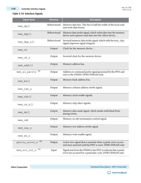
Table 5-14: Interface Signals<br />
emi_rm_004<br />
2013.12.16<br />
Signal Name<br />
mem_dq[]<br />
mem_dqs[]<br />
mem_dqs_n[]<br />
mem_ck<br />
mem_ck_n<br />
mem_addr[]<br />
mem_ac_parity (1)<br />
mem_ba[]<br />
mem_cas_n<br />
mem_cke[]<br />
mem_cs_n[]<br />
mem_dm[]<br />
mem_odt<br />
mem_ras_n<br />
mem_we_n<br />
parity_error_n (1)<br />
mem_err_out_n (1)<br />
Direction<br />
Bidirectional<br />
Bidirectional<br />
Bidirectional<br />
Output<br />
Output<br />
Output<br />
Output<br />
Output<br />
Output<br />
Output<br />
Output<br />
Output<br />
Output<br />
Output<br />
Output<br />
Output<br />
Input<br />
<strong>Description</strong><br />
<strong>Memory</strong> data bus. This bus is half the width of the local read<br />
and write data busses.<br />
<strong>Memory</strong> data strobe signal, which writes data into the memory<br />
device and captures read data into the <strong>Altera</strong> device.<br />
Inverted memory data strobe signal, which with the mem_dqs<br />
signal improves signal integrity.<br />
Clock for the memory device.<br />
Inverted clock for the memory device.<br />
<strong>Memory</strong> address bus.<br />
Address or command parity signal generated by the PHY and<br />
sent to the DIMM. DDR3 SDRAM only.<br />
<strong>Memory</strong> bank address bus.<br />
<strong>Memory</strong> column address strobe signal.<br />
<strong>Memory</strong> clock enable signals.<br />
<strong>Memory</strong> chip select signals.<br />
<strong>Memory</strong> data mask signal, which masks individual bytes<br />
during writes.<br />
<strong>Memory</strong> on-die termination control signal.<br />
<strong>Memory</strong> row address strobe signal.<br />
<strong>Memory</strong> write enable signal.<br />
Active-low signal that is asserted when a parity error occurs<br />
and stays asserted until the PHY is reset. DDR3 SDRAM only<br />
Signal sent from the DIMM to the PHY to indicate that a parity<br />
error has occured for a particular cycle. DDR3 SDRAM only.<br />
<strong>Altera</strong> Corporation<br />
<strong>Functional</strong> <strong>Description</strong>—<strong>HPC</strong> <strong>II</strong> <strong>Controller</strong><br />
Send Feedback


