Functional Description -- HPC II Controller, External Memory ... - Altera
Functional Description -- HPC II Controller, External Memory ... - Altera
Functional Description -- HPC II Controller, External Memory ... - Altera
You also want an ePaper? Increase the reach of your titles
YUMPU automatically turns print PDFs into web optimized ePapers that Google loves.
emi_rm_004<br />
2013.12.16<br />
Command Generator<br />
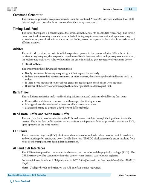
The command generator accepts commands from the front-end Avalon-ST interface and from local ECC<br />
internal logic, and provides those commands to the timing bank pool.<br />
Timing Bank Pool<br />
The timing bank pool is a parallel queue that works with the arbiter to enable data reordering. The timing<br />
bank pool tracks incoming requests, ensures that all timing requirements are met and, upon receiving<br />
write-data-ready notification from the write data buffer, passes the requests to the arbiter in an ordered and<br />
efficient manner.<br />
Arbiter<br />
The arbiter determines the order in which requests are passed to the memory device. When the arbiter<br />
receives a single request, that request is passed immediately; however, when multiple requests are received,<br />
the arbiter uses arbitration rules to determine the order in which to pass requests to the memory device.<br />
Arbitration Rules<br />
The arbiter uses the following arbitration rules:<br />
• If only one master is issuing a request, grant that request immediately.<br />
• If there are outstanding requests from two or more masters, the arbiter applies the following tests, in<br />
order:<br />
• Is there a read request? If so, the arbiter grants the read request ahead of any write requests.<br />
• If neither of the above conditions apply, the arbiter grants the oldest request first.<br />
Rank Timer<br />
The rank timer maintains rank-specific timing information, and performs the following functions:<br />
• Ensures that only four activates occur within a specified timing window.<br />
• Manages the read-to-write and write-to-read bus turnaround time.<br />
• Manages the time-to-activate delay between different banks.<br />
Read Data Buffer and Write Data Buffer<br />
The read data buffer receives data from the PHY and passes that data through the input interface to the<br />
master. The write data buffer receives write data from the input interface and passes that data to the PHY,<br />
upon approval of the write request.<br />
ECC Block<br />
The error-correcting code (ECC) block comprises an encoder and a decoder-corrector, which can detect<br />
and correct single-bit errors, and detect double-bit errors. The ECC block can remedy errors resulting from<br />
noise or other impairments during data transmission.<br />
AFI and CSR Interfaces<br />
The AFI interface provides communication between the controller and the physical layer logic (PHY). The<br />
CSR interface provides communication with your system’s internal control status registers.<br />
For more information about AFI signals, refer to AFI 3.0 Specification in the <strong>Functional</strong> <strong>Description</strong> - UniPHY<br />
chapter.<br />
Note:<br />
Unaligned reads and writes on the AFI interface are not supported.<br />
Command Generator<br />
5-5<br />
<strong>Functional</strong> <strong>Description</strong>—<strong>HPC</strong> <strong>II</strong> <strong>Controller</strong><br />
<strong>Altera</strong> Corporation<br />
Send Feedback


