Functional Description -- HPC II Controller, External Memory ... - Altera
Functional Description -- HPC II Controller, External Memory ... - Altera
Functional Description -- HPC II Controller, External Memory ... - Altera
You also want an ePaper? Increase the reach of your titles
YUMPU automatically turns print PDFs into web optimized ePapers that Google loves.
5-20<br />
Local Interface Signals<br />
emi_rm_004<br />
2013.12.16<br />
Signal Name<br />
Direction<br />
<strong>Description</strong><br />
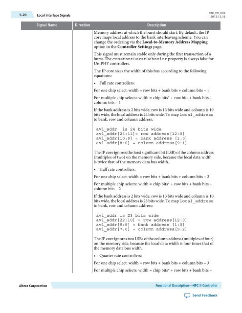
<strong>Memory</strong> address at which the burst should start. By default, the IP<br />
core maps local address to the bank interleaving scheme. You can<br />
change the ordering via the Local-to-<strong>Memory</strong> Address Mapping<br />
option in the <strong>Controller</strong> Settings page.<br />
This signal must remain stable only during the first transaction of a<br />
burst. The constantBurstBehavior property is always false for<br />
UniPHY controllers.<br />
The IP core sizes the width of this bus according to the following<br />
equations:<br />
• Full rate controllers:<br />
For one chip select: width = row bits + bank bits + column bits – 1<br />
For multiple chip selects: width = chip bits* + row bits + bank bits +<br />
column bits – 1<br />
If the bank address is 2 bits wide, row is 13 bits wide and column is 10<br />
bits wide, the local address is 24 bits wide. To map local_address<br />
to bank, row and column address:<br />
avl_addr is 24 bits wide<br />
avl_addr[23:11]= row address[12:0]<br />
avl_addr[10:9] = bank address [1:0]<br />
avl_addr[8:0] = column address[9:1]<br />
The IP core ignores the least significant bit (LSB) of the column address<br />
(multiples of two) on the memory side, because the local data width<br />
is twice that of the memory data bus width.<br />
• Half rate controllers:<br />
For one chip select: width = row bits + bank bits + column bits – 2<br />
For multiple chip selects: width = chip bits* + row bits + bank bits +<br />
column bits – 2<br />
If the bank address is 2 bits wide, row is 13 bits wide and column is 10<br />
bits wide, the local address is 23 bits wide. To map local_address<br />
to bank, row and column address:<br />
avl_addr is 23 bits wide<br />
avl_addr[22:10] = row address[12:0]<br />
avl_addr[9:8] = bank address [1:0]<br />
avl_addr[7:0] = column address[9:2]<br />
The IP core ignores two LSBs of the column address (multiples of four)<br />
on the memory side, because the local data width is four times that of<br />
the memory data bus width.<br />
• Quarter rate controllers:<br />
For one chip select: width = row bits + bank bits + column bits – 3<br />
For multiple chip selects: width = chip bits* + row bits + bank bits +<br />
<strong>Altera</strong> Corporation<br />
<strong>Functional</strong> <strong>Description</strong>—<strong>HPC</strong> <strong>II</strong> <strong>Controller</strong><br />
Send Feedback


