Pin-Outs - Altera
Pin-Outs - Altera
Pin-Outs - Altera
Create successful ePaper yourself
Turn your PDF publications into a flip-book with our unique Google optimized e-Paper software.
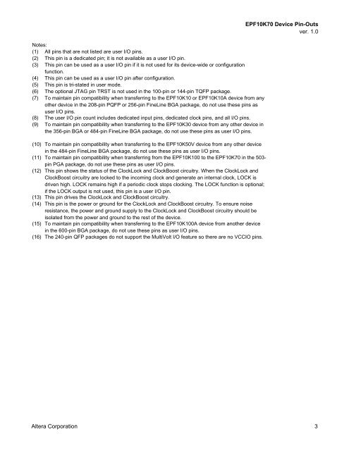
Notes:<br />
(1) All pins that are not listed are user I/O pins.<br />
(2) This pin is a dedicated pin; it is not available as a user I/O pin.<br />
(3) This pin can be used as a user I/O pin if it is not used for its device-wide or configuration<br />
function.<br />
(4) This pin can be used as a user I/O pin after configuration.<br />
(5) This pin is tri-stated in user mode.<br />
(6) The optional JTAG pin TRST is not used in the 100-pin or 144-pin TQFP package.<br />
(7) To maintain pin compatibility when transferring to the EPF10K10 or EPF10K10A device from any<br />
other device in the 208-pin PQFP or 256-pin FineLine BGA package, do not use these pins as<br />
user I/O pins.<br />
(8) The user I/O pin count includes dedicated input pins, dedicated clock pins, and all I/O pins.<br />
(9) To maintain pin compatibility when transferring to the EPF10K30 device from any other device in<br />
the 356-pin BGA or 484-pin FineLine BGA package, do not use these pins as user I/O pins.<br />
(10) To maintain pin compatibility when transferring to the EPF10K50V device from any other device<br />
in the 484-pin FineLine BGA package, do not use these pins as user I/O pins.<br />
(11) To maintain pin compatibility when transferring from the EPF10K100 to the EPF10K70 in the 503pin<br />
PGA package, do not use these pins as user I/O pins.<br />
(12) This pin shows the status of the ClockLock and ClockBoost circuitry. When the ClockLock and<br />
ClockBoost circuitry are locked to the incoming clock and generate an internal clock, LOCK is<br />
driven high. LOCK remains high if a periodic clock stops clocking. The LOCK function is optional;<br />
if the LOCK output is not used, this pin is a user I/O pin.<br />
(13) This pin drives the ClockLock and ClockBoost circuitry.<br />
(14) This pin is the power or ground for the ClockLock and ClockBoost circuitry. To ensure noise<br />
resistance, the power and ground supply to the ClockLock and ClockBoost circuitry should be<br />
isolated from the power and ground to the rest of the device.<br />
(15) To maintain pin compatibility when transferring to the EPF10K100A device from another device<br />
in the 600-pin BGA package, do not use these pins as user I/O pins.<br />
(16) The 240-pin QFP packages do not support the MultiVolt I/O feature so there are no VCCIO pins.<br />
EPF10K70 Device <strong>Pin</strong>-<strong>Outs</strong><br />
ver. 1.0<br />
<strong>Altera</strong> Corporation 3


