
You also want an ePaper? Increase the reach of your titles
YUMPU automatically turns print PDFs into web optimized ePapers that Google loves.
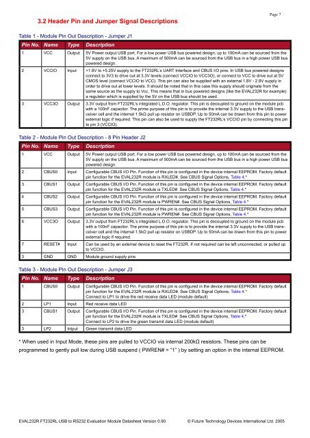
3.2 Header Pin and Jumper Signal Descriptions<br />
Table 1 - Module Pin Out Description - Jumper J1<br />
Pin No. Name Type Description<br />
1 VCC Output 5V Power output USB port. For a low power USB bus powered design, up to 100mA can be sourced from the<br />
5V supply on the USB bus. A maximum of 500mA can be sourced from the USB bus in a high power USB bus<br />
powered design.<br />
2 VCCIO Input +1.8V to +5.25V supply to the FT232RL’s UART Interface and CBUS I/O pins. In USB bus powered designs<br />
connect to 3V3 to drive out at 3.3V levels (connect VCCIO to VCC3O), or connect to VCC to drive out at 5V<br />
CMOS level (connect VCCIO to VCC). This pin can also be supplied with an external 1.8V - 2.8V supply in<br />
order to drive out at lower levels. It should be noted that in this case this supply should originate from the<br />
same source as the supply to Vcc. This means that in bus powered designs (like the <strong>EVAL232R</strong> for example)<br />
a regulator which is supplied by the 5V on the USB bus should be used.<br />
3 VCC3O Output 3.3V output from FT232RL’s integrated L.D.O. regulator. This pin is decoupled to ground on the module pcb<br />
with a 100nF capacitor. The prime purpose of this pin is to provide the internal 3.3V supply to the USB transceiver<br />
cell and the internal 1.5kΩ pull up resistor on USBDP. Up to 50mA can be drawn from this pin to power<br />
external logic if required. This pin can also be used to supply the FT232RL’s VCCIO pin by connecting this pin<br />
to pin 3 (VCCIO).<br />
Table 2 - Module Pin Out Description - 8 Pin Header J2<br />
Pin No. Name Type Description<br />
1 VCC Output 5V Power output USB port. For a low power USB bus powered design, up to 100mA can be sourced from the<br />
5V supply on the USB bus. A maximum of 500mA can be sourced from the USB bus in a high power USB bus<br />
powered design.<br />
2 CBUS0 Input Configurable CBUS I/O Pin. Function of this pin is configured in the device internal EEPROM. Factory default<br />
pin function for the <strong>EVAL232R</strong> module is RXLED#. See CBUS Signal Options, Table 4.*<br />
3 CBUS1 Output Configurable CBUS I/O Pin. Function of this pin is configured in the device internal EEPROM. Factory default<br />
pin function for the <strong>EVAL232R</strong> module is TXLED#. See CBUS Signal Options, Table 4.*<br />
4 CBUS2 Output Configurable CBUS I/O Pin. Function of this pin is configured in the device internal EEPROM. Factory default<br />
pin function for the <strong>EVAL232R</strong> module is PWREN#. See CBUS Signal Options, Table 4.*<br />
5 CBUS3 Output Configurable CBUS I/O Pin. Function of this pin is configured in the device internal EEPROM. Factory default<br />
pin function for the <strong>EVAL232R</strong> module is PWREN#. See CBUS Signal Options, Table 4.*<br />
6 VCC3O Output 3.3V output from FT232RL’s integrated L.D.O. regulator. This pin is decoupled to ground on the module pcb<br />
with a 100nF capacitor. The prime purpose of this pin is to provide the internal 3.3V supply to the USB transceiver<br />
cell and the internal 1.5kΩ pull up resistor on USBDP. Up to 50mA can be drawn from this pin to power<br />
external logic if required.<br />
7 RESET# Input Can be used by an external device to reset the FT232R. If not required can be left unconnected, or pulled up<br />
to VCCIO.<br />
3 GND GND Module ground supply pins<br />
Table 3 - Module Pin Out Description - Jumper J3<br />
Pin No. Name Type Description<br />
1 CBUS0 Output Configurable CBUS I/O Pin. Function of this pin is configured in the device internal EEPROM. Factory default<br />
pin function for the <strong>EVAL232R</strong> module is RXLED#. See CBUS Signal Options, Table 4.*<br />
Connect to LP1 to drive the red receive data LED (module default)<br />
2 LP1 Input Red receive data LED<br />
3 CBUS1 Output Configurable CBUS I/O Pin. Function of this pin is configured in the device internal EEPROM. Factory default<br />
pin function for the <strong>EVAL232R</strong> module is TXLED#. See CBUS Signal Options, Table 4.*<br />
Connect to LP2 to drive the green transmit data LED (module default)<br />
3 LP2 Intput Green transmit data LED<br />
* When used in Input Mode, these pins are pulled to VCCIO via internal 200kΩ resistors. These pins can be<br />
programmed to gently pull low during USB suspend ( PWREN# = “1” ) by setting an option in the internal EEPROM.<br />
<strong>EVAL232R</strong> FT232RL USB to RS232 Evaluation Module <strong>Datasheet</strong> Version 0.90 © Future Technology Devices International Ltd. 2005<br />
Page 7