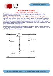
3.3 CBUS Signal Options The following options can be configured on the CBUS I/O pins. These options are all configured in the internal EEPROM using the utility software MPROG, which can be downloaded from the <strong>FTDI</strong> website. The default configuration is described in Section 8. Table 4 - CBUS Signal Options CBUS Signal Option Available On CBUS Pin... Description TXDEN CBUS0, CBUS1, CBUS2, CBUS3, CBUS4 Enable transmit data for RS485 TXLED# CBUS0, CBUS1, CBUS2, CBUS3, CBUS4 Transmit data LED drive - pulses low when transmitting data via USB. See FT232R datasheet for more details. RXLED# CBUS0, CBUS1, CBUS2, CBUS3, CBUS4 Receive data LED drive - pulses low when receiving data via USB. See FT232R datasheet for more details. TX&RXLED# CBUS0, CBUS1, CBUS2, CBUS3, CBUS4 LED drive - pulses low when transmitting or receiving data via USB. See FT232R datasheet for more details. PWREN# CBUS0, CBUS1, CBUS2, CBUS3, CBUS4 Goes low after the device is configured by USB, then high during USB suspend. Can be used to control power to external logic P- Channel logic level MOSFET switch. Enable the interface pull-down option when using the PWREN# pin in this way. SLEEP# CBUS0, CBUS1, CBUS2, CBUS3, CBUS4 Goes low during USB suspend mode. Typically used to power down an external TTL to RS232 level converter I.C. in USB to RS232 converter designs. CLK48 CBUS0, CBUS1, CBUS2, CBUS3, CBUS4 48MHz Clock output. CLK24 CBUS0, CBUS1, CBUS2, CBUS3, CBUS4 24MHz Clock output. CLK12 CBUS0, CBUS1, CBUS2, CBUS3, CBUS4 12MHz Clock output. CLK6 CBUS0, CBUS1, CBUS2, CBUS3, CBUS4 6MHz Clock output. CBitBangI/O CBUS0, CBUS1, CBUS2, CBUS3 CBUS bit bang mode option. Allows up to 4 of the CBUS pins to be used as general purpose I/O. Configured individually for CBUS0, CBUS1, CBUS2 and CBUS3 in the internal EEPROM. A separate application note will describe in more detail how to use CBUS bit bang mode. BitBangWRn CBUS0, CBUS1, CBUS2, CBUS3 Synchronous and asynchronous bit bang mode WR# strobe Output BitBangRDn CBUS0, CBUS1, CBUS2, CBUS3 Synchronous and asynchronous bit bang mode RD# strobe Output 3.4 RS232 Signal Descriptions Table 5 - RS232 Signals DB9 pin No. Name Type Description 1 DCD Input Data Carrier Detect control input 2 RXDATA Input Receive Asynchronous Data input. 3 TXDATA Output Transmit Asynchronous Data output. 4 DTR Output Data Terminal Ready control output / Handshake signal 5 GND GND Device groud supply pin. 6 DSR Input Data Set Ready control input / Handshake signal 7 RTS Output Request To Send Control Output / Handshake signal. 8 CTS Input Clear to Send Control input / Handshake signal. 9 RI Input Ring Indicator control input. When remote wakeup is enabled in the FT232RL’s internal EEPROM taking RI# low can be used to resume the PC USB host controller from suspend. <strong>EVAL232R</strong> FT232RL USB to RS232 Evaluation Module <strong>Datasheet</strong> Version 0.90 © Future Technology Devices International Ltd. 2005 Page 8
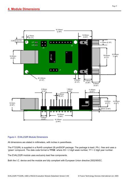
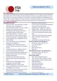
4. Module Dimensions 3.25mm (0.13") 12.00mm (0.48") 12.5mm (0.50") 2.75mm (0.11") LP1 LP2 Figure 4 - <strong>EVAL232R</strong> Module Dimensions All dimensions are stated in millimeters, with inches in parenthesis. The FT232RL is supplied in a RoHS compliant 28 pinSSOP package. The package is lead ( Pb ) free and uses a ‘green’ compound. The date code format is YYXX where XX = 2 digit week number, YY = 2 digit year number. The <strong>EVAL232R</strong> module uses exclusivly lead free components. J3 Ø 2.50mm (0.10") 2.55mm (0.10") 4.95mm (0.20") <strong>FTDI</strong> 61.50mm (2.46") 3.25mm (0.13") 12.50mm (0.50") 7.00mm (0.28") 5.50mm (0.22") Both the I.C. device and the module are fully compliant with European Union directive 2002/95/EC. J1 0.65mm (0.03") 20.00mm (0.80") 61.00mm (2.44") 18.00mm (0.72") <strong>EVAL232R</strong> FT232RL USB to RS232 Evaluation Module <strong>Datasheet</strong> Version 0.90 © Future Technology Devices International Ltd. 2005 J2 1.90mm (0.08") 11.80mm (0.47") 4.70mm (0.19") 9.30mm (0.37") 1.60mm (0.06") Page 9 32.00mm (1.28") 14.35mm (0.57")