Why Silicon Photonics? - Institute of Microelectronics - A*Star
Why Silicon Photonics? - Institute of Microelectronics - A*Star
Why Silicon Photonics? - Institute of Microelectronics - A*Star

Create successful ePaper yourself
Turn your PDF publications into a flip-book with our unique Google optimized e-Paper software.
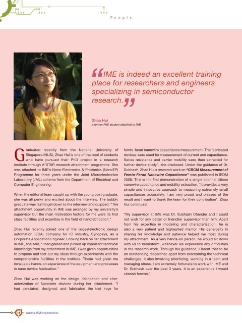
People<br />
IME is indeed an excellent training<br />
place for researchers and engineers<br />
specializing in semiconductor<br />
research.<br />
Zhao Hui<br />
a former PhD student attached to IME.<br />
Graduated recently from the National University <strong>of</strong><br />
Singapore (NUS), Zhao Hui is one <strong>of</strong> the pool <strong>of</strong> students<br />
who have pursued their PhD project in a research<br />
institute through A*STAR research attachment programme. She<br />
was attached to IME’s Nano-Electronics & <strong>Photonics</strong> (NanoEP)<br />
Programme for three years under the Joint <strong>Microelectronics</strong><br />
Laboratory (JML) scheme from the Department <strong>of</strong> Electrical and<br />
Computer Engineering.<br />
When the editorial team caught up with the young post graduate,<br />
she was all perky and excited about the interview. The bubbly<br />
graduate was fast to get down to the interview and quipped, “The<br />
attachment opportunity in IME was arranged by my university’s<br />
supervisor but the main motivation factors for me were its first<br />
class facilities and expertise in the field <strong>of</strong> nan<strong>of</strong>abrication.”<br />
Zhao Hui recently joined one <strong>of</strong> the largestelectronic design<br />
automation (EDA) company for IC industry, Synopsys, as a<br />
Corporate Application Engineer. Looking back on her attachment<br />
in IME, she said, “I had gained and picked up important technical<br />
knowledge from my attachment in IME. I was given opportunities<br />
to propose and test out my ideas through experiments with the<br />
comprehensive facilities in the institute. These had given me<br />
invaluable hands-on experience <strong>of</strong> the equipment and processes<br />
in nano device fabrication.”<br />
Zhao Hui was working on the design, fabrication and characterization<br />
<strong>of</strong> Nanowire devices during her attachment. “I<br />
had simulated, designed, and fabricated the test keys for<br />
femto-farad nanowire capacitance measurement. The fabricated<br />
devices were used for measurement <strong>of</strong> current and capacitance.<br />
Series resistance and carrier mobility were then extracted for<br />
further device study”, she disclosed. Under the guidance <strong>of</strong> Dr.<br />
Subhash, Zhao Hui’s research work on “CBCM Measurement <strong>of</strong><br />
Femto-Farad Nanowire Capacitance” was published in IEDM<br />
2008. This is the first demonstration <strong>of</strong> a single channel silicon<br />
nanowire capacitance and mobility extraction. “It provides a very<br />
simple and innovative approach to measuring extremely small<br />
capacitances accurately. I am very proud and pleased <strong>of</strong> the<br />
result and I want to thank the team for their contribution”, Zhao<br />
Hui continued.<br />
”My supervisor at IME was Dr. Subhash Chander and I could<br />
not wish for any better or friendlier supervisor than him. Apart<br />
from his expertise in modeling and characterization, he is<br />
also a very patient and bighearted mentor. His generosity in<br />
sharing his knowledge and patience helped me most during<br />
my attachment. As a very hands-on person, he would sit down<br />
with us to brainstorm, whenever we experience any difficulties<br />
in the research work. Through his guidance, I learnt that to be<br />
an outstanding researcher, apart from overcoming the technical<br />
challenges, it also involving prioritizing, working in a team and<br />
managing stress. I am extremely fortunate to work with IME and<br />
Dr. Subhash over the past 3 years. It is an experience I would<br />
cherish forever.”<br />
18 <strong>Institute</strong> <strong>of</strong> <strong>Microelectronics</strong>