Why Silicon Photonics? - Institute of Microelectronics - A*Star
Why Silicon Photonics? - Institute of Microelectronics - A*Star
Why Silicon Photonics? - Institute of Microelectronics - A*Star

You also want an ePaper? Increase the reach of your titles
YUMPU automatically turns print PDFs into web optimized ePapers that Google loves.
Cover<br />
Story<br />
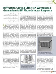
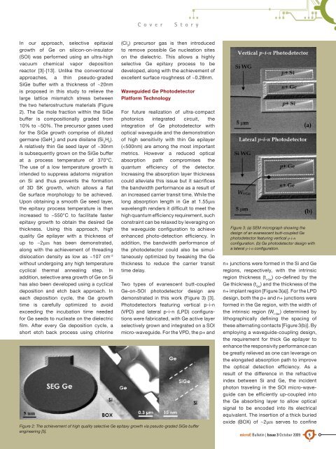
In our approach, selective epitaxial<br />
growth <strong>of</strong> Ge on silicon-on-insulator<br />
(SOI) was performed using an ultra-high<br />
vacuum chemical vapor deposition<br />
reactor [3]-[13]. Unlike the conventional<br />
approaches, a thin pseudo-graded<br />
SiGe buffer with a thickness <strong>of</strong> ~20nm<br />
is proposed in this study to relieve the<br />
large lattice mismatch stress between<br />
the two heterostructure materials (Figure<br />
2). The Ge mole fraction within the SiGe<br />
buffer is compositionally graded from<br />
10% to ~50%. The precursor gases used<br />
for the SiGe growth comprise <strong>of</strong> diluted<br />
germane (GeH 4<br />
) and pure disilane (Si 2<br />
H 6<br />
).<br />
A relatively thin Ge seed layer <strong>of</strong> ~30nm<br />
is subsequently grown on the SiGe buffer<br />
at a process temperature <strong>of</strong> 370°C.<br />
The use <strong>of</strong> a low temperature growth is<br />
intended to suppress adatoms migration<br />
on Si and thus prevents the formation<br />
<strong>of</strong> 3D SK growth, which allows a flat<br />
Ge surface morphology to be achieved.<br />
Upon obtaining a smooth Ge seed layer,<br />
the epitaxy process temperature is then<br />
increased to ~550°C to facilitate faster<br />
epitaxy growth to obtain the desired Ge<br />
thickness. Using this approach, high<br />
quality Ge epilayer with a thickness <strong>of</strong><br />
up to ~2μm has been demonstrated,<br />
along with the achievement <strong>of</strong> threading<br />
dislocation density as low as ~107 cm -2<br />
without undergoing any high temperature<br />
cyclical thermal annealing step. In<br />
addition, selective area growth <strong>of</strong> Ge on Si<br />
has also been developed using a cyclical<br />
deposition and etch back approach. In<br />
each deposition cycle, the Ge growth<br />
time is carefully optimized to avoid<br />
exceeding the incubation time needed<br />
for Ge seeds to nucleate on the dielectric<br />
film. After every Ge deposition cycle, a<br />
short etch back process using chlorine<br />
(Cl 2<br />
) precursor gas is then introduced<br />
to remove possible Ge nucleation sites<br />
on the dielectric. This allows a highly<br />
selective Ge epitaxy process to be<br />
developed, along with the achievement <strong>of</strong><br />
excellent surface roughness <strong>of</strong> ~0.28nm.<br />
Waveguided Ge Photodetector<br />
Platform Technology<br />
For future realization <strong>of</strong> ultra-compact<br />
photonics integrated circuit, the<br />
integration <strong>of</strong> Ge photodetector with<br />
optical waveguide and the demonstration<br />
<strong>of</strong> high sensitivity with thin Ge epilayer<br />
(