Why Silicon Photonics? - Institute of Microelectronics - A*Star
Why Silicon Photonics? - Institute of Microelectronics - A*Star
Why Silicon Photonics? - Institute of Microelectronics - A*Star

You also want an ePaper? Increase the reach of your titles
YUMPU automatically turns print PDFs into web optimized ePapers that Google loves.
Cover<br />
Story<br />
the optical mode within the core <strong>of</strong> the Si<br />
waveguide so as to prevent leakage into<br />
the underneath Si substrate.<br />
Performance Metrics <strong>of</strong> Waveguided<br />
Ge Photodetector<br />
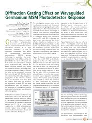
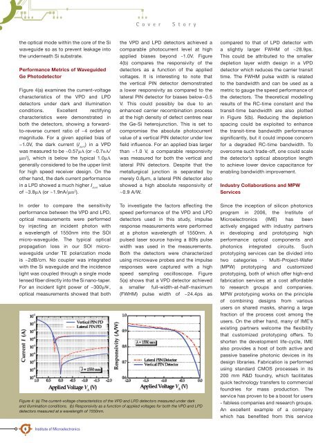
Figure 4(a) examines the current-voltage<br />
characteristics <strong>of</strong> the VPD and LPD<br />
detectors under dark and illumination<br />
conditions. Excellent rectifying<br />
characteristics were demonstrated in<br />
both the detectors, showing a forwardto-reverse<br />
current ratio <strong>of</strong> ~4 orders <strong>of</strong><br />
magnitude. For a given applied bias <strong>of</strong><br />
−1.0V, the dark current (I dark<br />
) in a VPD<br />
was measured to be ~0.57μA (or ~0.7nA/<br />
μm 2 ), which is below the typical 1.0μA<br />
generally considered to be the upper limit<br />
for high speed receiver design. On the<br />
other hand, the dark current performance<br />
in a LPD showed a much higher I dark<br />
value<br />
<strong>of</strong> ~3.8μA (or ~1.9nA/μm 2 ).<br />
the VPD and LPD detectors achieved a<br />
comparable photocurrent level at high<br />
applied biases beyond -1.0V. Figure<br />
4(b) compares the responsivity <strong>of</strong> the<br />
detectors as a function <strong>of</strong> the applied<br />
voltages. It is interesting to note that<br />
the vertical PIN detector demonstrated<br />
a lower responsivity as compared to the<br />
lateral PIN detector for biases below−0.5<br />
V. This could possibly be due to an<br />
enhanced carrier recombination process<br />
at the high density <strong>of</strong> defect centres near<br />
the Ge-Si heterojunction. This is set to<br />
compromise the absolute photocurrent<br />
value <strong>of</strong> a vertical PIN detector under low<br />
field influence. For an applied bias larger<br />
than −1.0 V, a comparable responsivity<br />
was measured for both the vertical and<br />
lateral PIN detectors. Despite that the<br />
metallurgical junction is separated by<br />
merely 0.8μm, a lateral PIN detector also<br />
showed a high absolute responsivity <strong>of</strong><br />
~0.9 A/W.<br />
compared to that <strong>of</strong> LPD detector with<br />
a slightly larger FWHM <strong>of</strong> ~28.9ps.<br />
This could be attributed to the smaller<br />
depletion layer width design in a VPD<br />
detector which reduces the carrier transit<br />
time. The FWHM pulse width is related<br />
to the bandwidth and can be used as a<br />
metric to gauge the speed performance <strong>of</strong><br />
the detectors. The theoretical modelling<br />
results <strong>of</strong> the RC-time constant and the<br />
transit-time bandwidth are also plotted<br />
in Figure 5(b). Reducing the depletion<br />
spacing could be exploited to enhance<br />
the transit-time bandwidth performance<br />
significantly, but it could impose concern<br />
for a degraded RC-time bandwidth. To<br />
overcome such trade-<strong>of</strong>f, one could scale<br />
the detector’s optical absorption length<br />
to achieve lower device capacitance for<br />
enabling bandwidth improvement.<br />
Industry Collaborations and MPW<br />
Services<br />
In order to compare the sensitivity<br />
performance between the VPD and LPD,<br />
optical measurements were performed<br />
by injecting an incident photon with<br />
a wavelength <strong>of</strong> 1550nm into the SOI<br />
micro-waveguide. The typical optical<br />
propagation loss in our SOI microwaveguide<br />
under TE polarization mode<br />
is ~2dB/cm. No coupler was integrated<br />
with the Si waveguide and the incidence<br />
light was coupled through a single mode<br />
lensed fiber directly into the Si nano-taper.<br />
For an incident light power <strong>of</strong> ~300μW,<br />
optical measurements showed that both<br />
To investigate the factors affecting the<br />
speed performance <strong>of</strong> the VPD and LPD<br />
detectors used in this study, impulse<br />
response measurements were performed<br />
at a photon wavelength <strong>of</strong> 1550nm. A<br />
pulsed laser source having a 80fs pulse<br />
width was used in the measurements.<br />
Both the detectors were characterized<br />
using microwave probes and the impulse<br />
responses were captured with a high<br />
speed sampling oscilloscope. Figure<br />
5(a) shows that a VPD detector achieved<br />
a smaller full-width-at-half-maximum<br />
(FWHM) pulse width <strong>of</strong> ~24.4ps as<br />
Figure 4: (a) The current-voltage characteristics <strong>of</strong> the VPD and LPD detectors measured under dark<br />
and illumination conditions. (b) Responsivity as a function <strong>of</strong> applied voltages for both the VPD and LPD<br />
detectors measured at a wavelength <strong>of</strong> 1550nm.<br />
Since the inception <strong>of</strong> silicon photonics<br />
program in 2006, the <strong>Institute</strong> <strong>of</strong><br />
<strong>Microelectronics</strong> (IME) has been<br />
actively engaged with industry partners<br />
in developing and prototyping high<br />
performance optical components and<br />
photonics integrated circuits. Such<br />
prototyping services can be divided into<br />
two categories - Multi-Project-Wafer<br />
(MPW) prototyping and customized<br />
prototyping, both <strong>of</strong> which <strong>of</strong>fer high-end<br />
fabrication services at a cost affordable<br />
to research groups and companies.<br />
MPW prototyping works on the principle<br />
<strong>of</strong> combining designs from various<br />
users on shared masks, sharing a large<br />
fraction <strong>of</strong> the process cost among the<br />
users. On the other hand, many <strong>of</strong> IME’s<br />
existing partners welcome the flexibility<br />
that customized prototyping <strong>of</strong>fers. To<br />
shorten the development life-cycle, IME<br />
also provides a host <strong>of</strong> both active and<br />
passive baseline photonic devices in its<br />
design libraries. Fabrication is performed<br />
using standard CMOS processes in its<br />
200 mm R&D foundry, which facilitates<br />
quick technology transfers to commercial<br />
foundries for mass production. The<br />
service has proven to be a boost for users<br />
- fabless companies and research groups.<br />
An excellent example <strong>of</strong> a company<br />
which has benefited from this service<br />
6 <strong>Institute</strong> <strong>of</strong> <strong>Microelectronics</strong>