design and implementation of thyristor switched shunt capacitors a ...
design and implementation of thyristor switched shunt capacitors a ...
design and implementation of thyristor switched shunt capacitors a ...

You also want an ePaper? Increase the reach of your titles
YUMPU automatically turns print PDFs into web optimized ePapers that Google loves.
ˆ I S is the peak value <strong>of</strong> the inrush current, (A);<br />
U is the phase to ground voltage, (V);<br />
X C is the series- connected capacitive reactance per phase, (Ω);<br />
X L is the inductive reactance per phase between the capacitor banks, (Ω);<br />
Q 1 is the output reactive power <strong>of</strong> the capacitor to be <strong>switched</strong> in, (MVAr);<br />
Q 2 is the sum <strong>of</strong> the output reactive power <strong>of</strong> the capacitor banks which are<br />
already energized, (MVAr).<br />
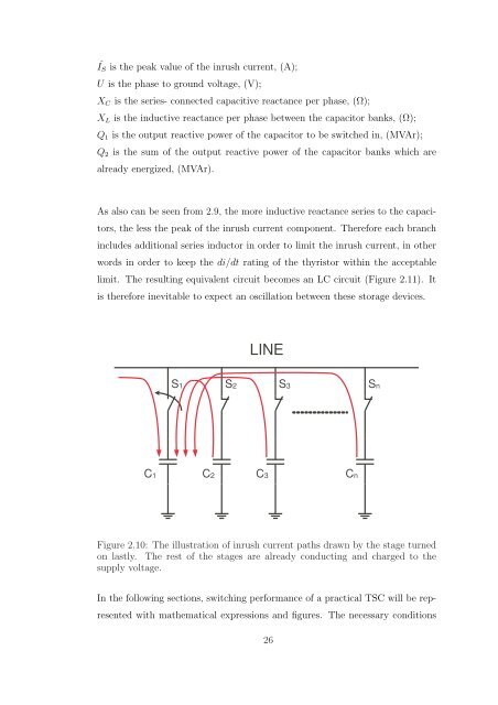
As also can be seen from 2.9, the more inductive reactance series to the <strong>capacitors</strong>,<br />
the less the peak <strong>of</strong> the inrush current component. Therefore each branch<br />
includes additional series inductor in order to limit the inrush current, in other<br />
words in order to keep the di/dt rating <strong>of</strong> the <strong>thyristor</strong> within the acceptable<br />
limit. The resulting equivalent circuit becomes an LC circuit (Figure 2.11). It<br />
is therefore inevitable to expect an oscillation between these storage devices.<br />
LINE<br />
S1 S2 S3 Sn<br />
C1 C2 C3 Cn<br />
Figure 2.10: The illustration <strong>of</strong> inrush current paths drawn by the stage turned<br />
on lastly. The rest <strong>of</strong> the stages are already conducting <strong>and</strong> charged to the<br />
supply voltage.<br />
In the following sections, switching performance <strong>of</strong> a practical TSC will be represented<br />
with mathematical expressions <strong>and</strong> figures. The necessary conditions<br />
26