tec.News - Harting
tec.News - Harting
tec.News - Harting

You also want an ePaper? Increase the reach of your titles
YUMPU automatically turns print PDFs into web optimized ePapers that Google loves.
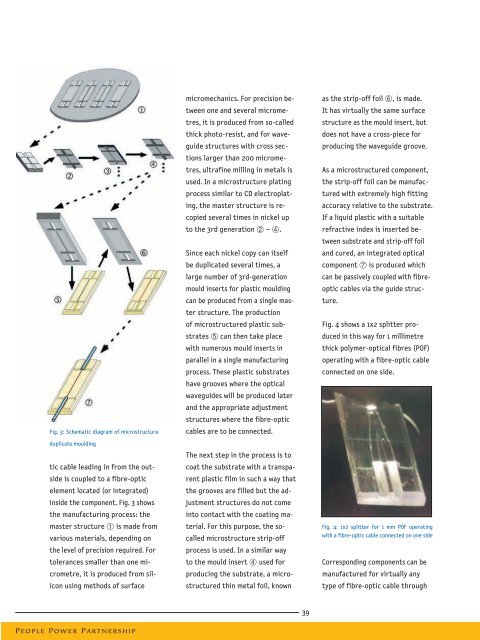
Fig. 3: Schematic diagram of microstructure<br />
duplicate moulding<br />
tic cable leading in from the outside<br />
is coupled to a fibre-optic<br />
element located (or integrated)<br />
inside the component. Fig. 3 shows<br />
the manufacturing process: the<br />
master structure À is made from<br />
various materials, depending on<br />
the level of precision required. For<br />
tolerances smaller than one micrometre,<br />
it is produced from silicon<br />
using methods of surface<br />
micromechanics. For precision between<br />
one and several micrometres,<br />
it is produced from so-called<br />
thick photo-resist, and for waveguide<br />
structures with cross sections<br />
larger than 200 micrometres,<br />
ultrafine milling in metals is<br />
used. In a microstructure plating<br />
process similar to CD electroplating,<br />
the master structure is recopied<br />
several times in nickel up<br />
to the 3rd generation Á – Ã.<br />
Since each nickel copy can itself<br />
be duplicated several times, a<br />
large number of 3rd-generation<br />
mould inserts for plastic moulding<br />
can be produced from a single master<br />
structure. The production<br />
of microstructured plastic substrates<br />
Ä can then take place<br />
with numerous mould inserts in<br />
parallel in a single manufacturing<br />
process. These plastic substrates<br />
have grooves where the optical<br />
waveguides will be produced later<br />
and the appropriate adjustment<br />
structures where the fibre-optic<br />
cables are to be connected.<br />
The next step in the process is to<br />
coat the substrate with a transparent<br />
plastic film in such a way that<br />
the grooves are filled but the adjustment<br />
structures do not come<br />
into contact with the coating material.<br />
For this purpose, the socalled<br />
microstructure strip-off<br />
process is used. In a similar way<br />
to the mould insert à used for<br />
producing the substrate, a microstructured<br />
thin metal foil, known<br />
as the strip-off foil Å, is made.<br />
It has virtually the same surface<br />
structure as the mould insert, but<br />
does not have a cross-piece for<br />
producing the waveguide groove.<br />
As a microstructured component,<br />
the strip-off foil can be manufactured<br />
with extremely high fitting<br />
accuracy relative to the substrate.<br />
If a liquid plastic with a suitable<br />
refractive index is inserted between<br />
substrate and strip-off foil<br />
and cured, an integrated optical<br />
component Æ is produced which<br />
can be passively coupled with fibreoptic<br />
cables via the guide structure.<br />
Fig. 4 shows a 1x2 splitter produced<br />
in this way for 1 millimetre<br />
thick polymer-optical fibres (POF)<br />
operating with a fibre-optic cable<br />
connected on one side.<br />
Fig. 4: 1x2 splitter for 1 mm POF operating<br />
with a fibre-optic cable connected on one side<br />
Corresponding components can be<br />
manufactured for virtually any<br />
type of fibre-optic cable through<br />
39<br />
People Power Partnership