

MJL21193 - Silicon Power Transistors - HEStore.hu
MJL21193 - Silicon Power Transistors - HEStore.hu
MJL21193 - Silicon Power Transistors - HEStore.hu

Create successful ePaper yourself
Turn your PDF publications into a flip-book with our unique Google optimized e-Paper software.
<strong>MJL21193</strong>, MJL21194<br />
TYPICAL CHARACTERISTICS<br />
PNP <strong>MJL21193</strong><br />
NPN MJL21194<br />
3.0<br />
1.4<br />
SATURATION VOLTAGE (VOLTS)<br />
2.5<br />
2.0<br />
1.5<br />
1.0<br />
0.5<br />
0<br />
0.1<br />
T J = 25°C<br />
I C /I B = 10<br />
V CE(sat)<br />
1.2<br />
T J = 25°C<br />
I C /I B = 10<br />
V BE(sat) 0.4<br />
1.0<br />
0.8<br />
0.6<br />
0.2<br />
0<br />
1.0<br />
10<br />
100 0.1<br />
I C , COLLECTOR CURRENT (AMPS)<br />
SATURATION VOLTAGE (VOLTS)<br />
V BE(sat)<br />
V CE(sat)<br />
1.0<br />
10<br />
I C , COLLECTOR CURRENT (AMPS)<br />
100<br />
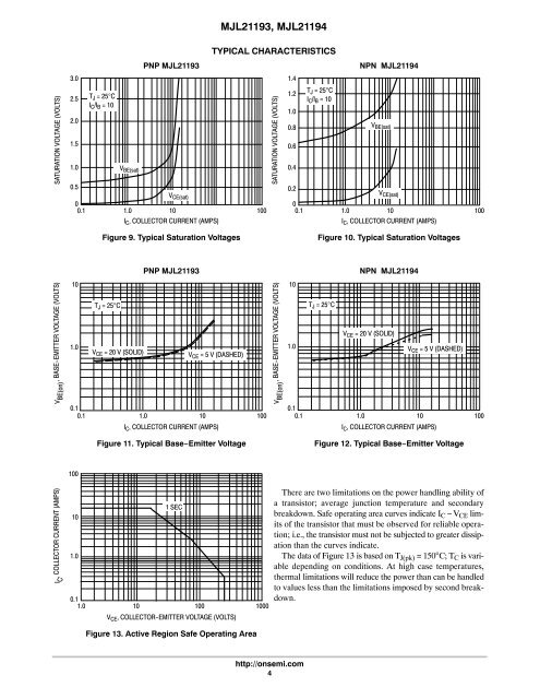
Figure 9. Typical Saturation Voltages<br />
Figure 10. Typical Saturation Voltages<br />
PNP <strong>MJL21193</strong><br />
NPN MJL21194<br />
V BE(on)<br />
, BASE-EMITTER VOLTAGE (VOLTS)<br />
10<br />
1.0<br />
0.1<br />
0.1<br />
T J = 25°C<br />
V CE = 20 V (SOLID)<br />
V CE = 5 V (DASHED)<br />
1.0<br />
10<br />
I C , COLLECTOR CURRENT (AMPS)<br />
100<br />
V BE(on)<br />
, BASE-EMITTER VOLTAGE (VOLTS)<br />
10<br />
1.0<br />
0.1<br />
0.1<br />
T J = 25°C<br />
V CE = 20 V (SOLID)<br />
V CE = 5 V (DASHED)<br />
1.0<br />
10<br />
I C , COLLECTOR CURRENT (AMPS)<br />
100<br />
Figure 11. Typical Base−Emitter Voltage<br />
Figure 12. Typical Base−Emitter Voltage<br />
100<br />
I C<br />
, COLLECTOR CURRENT (AMPS)<br />
10<br />
1.0<br />
1 SEC<br />
0.1<br />
1.0 10 100 1000<br />
V CE , COLLECTOR-EMITTER VOLTAGE (VOLTS)<br />
There are two limitations on the power handling ability of<br />
a transistor; average junction temperature and secondary<br />
breakdown. Safe operating area curves indicate I C − V CE limits<br />
of the transistor that must be observed for reliable operation;<br />
i.e., the transistor must not be subjected to greater dissipation<br />
than the curves indicate.<br />
The data of Figure 13 is based on T J(pk) = 150°C; T C is variable<br />
depending on conditions. At high case temperatures,<br />
thermal limitations will reduce the power than can be handled<br />
to values less than the limitations imposed by second breakdown.<br />
Figure 13. Active Region Safe Operating Area<br />
http://onsemi.com<br />
4


