

MJL21193 - Silicon Power Transistors - HEStore.hu
MJL21193 - Silicon Power Transistors - HEStore.hu
MJL21193 - Silicon Power Transistors - HEStore.hu

You also want an ePaper? Increase the reach of your titles
YUMPU automatically turns print PDFs into web optimized ePapers that Google loves.
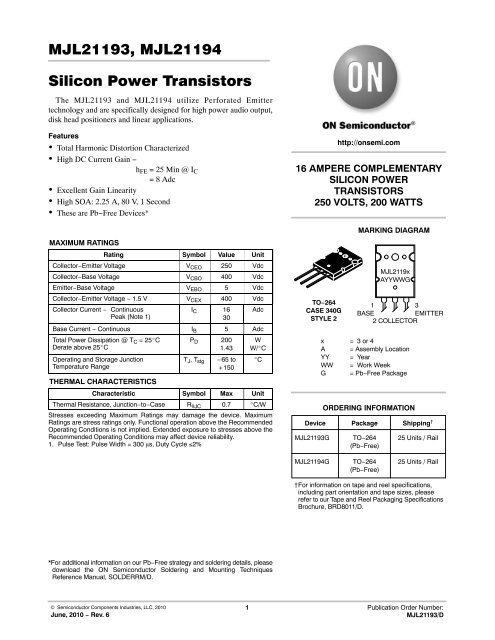
<strong>MJL21193</strong>, MJL21194<br />
<strong>Silicon</strong> <strong>Power</strong> <strong>Transistors</strong><br />
The <strong>MJL21193</strong> and MJL21194 utilize Perforated Emitter<br />
technology and are specifically designed for high power audio output,<br />
disk head positioners and linear applications.<br />
Features<br />
• Total Harmonic Distortion Characterized<br />
• High DC Current Gain −<br />
h FE = 25 Min @ I C<br />
= 8 Adc<br />
• Excellent Gain Linearity<br />
• High SOA: 2.25 A, 80 V, 1 Second<br />
• These are Pb−Free Devices*<br />
MAXIMUM RATINGS<br />
Rating<br />
Value Unit ÎÎÎ<br />
SymbolÎÎÎÎ<br />
ÎÎÎÎÎÎÎÎÎÎÎÎÎÎÎÎÎÎÎ<br />
ÎÎÎÎÎÎÎÎÎÎÎÎÎÎÎÎÎÎÎ<br />
Collector−Emitter Voltage<br />
V CEO 250 Vdc<br />
ÎÎÎ<br />
ÎÎÎÎÎÎÎÎÎÎÎÎ<br />
Collector−Base Voltage<br />
ÎÎÎ<br />
V CBO Vdc<br />
ÎÎÎÎ<br />
ÎÎÎÎÎÎÎÎÎÎÎÎ<br />
Emitter−Base Voltage<br />
ÎÎÎ<br />
V ÎÎÎÎ<br />
EBO 5 Vdc ÎÎÎ<br />
400 ÎÎÎ<br />
Collector−Emitter Voltage − 1.5 V<br />
V ÎÎÎ<br />
CEX 400 Vdc<br />
ÎÎÎÎ<br />
ÎÎÎÎÎÎÎÎÎÎÎÎ ÎÎÎ<br />
ÎÎÎÎÎÎÎÎÎÎÎÎ<br />
Collector Current − Continuous ÎÎÎ I ÎÎÎÎÎÎ<br />
C 16 Adc<br />
Peak (Note 1)<br />
ÎÎÎÎÎÎÎÎÎÎÎÎ ÎÎÎÎÎÎ<br />
ÎÎÎ<br />
Base Current − Continuous<br />
I B 5 Adc<br />
ÎÎÎÎÎÎÎÎÎÎÎÎÎÎ<br />
ÎÎÎÎ<br />
ÎÎÎ<br />
P D 200 W<br />
Total <strong>Power</strong> Dissipation @ T C = 25C<br />
Derate above 25C<br />
ÎÎÎÎÎÎÎÎÎÎÎÎ ÎÎÎÎÎÎ<br />
ÎÎÎ<br />
Operating and Storage Junction ÎÎÎ T ÎÎÎÎ<br />
ÎÎÎ<br />
ÎÎÎÎÎÎÎÎÎÎÎÎ J , T stg −65 to<br />
Temperature Range<br />
THERMAL CHARACTERISTICS<br />
30<br />
1.43<br />
+150<br />
W/C<br />
C<br />
ÎÎÎÎÎÎÎÎÎÎÎÎ ÎÎÎÎ<br />
ÎÎÎ ÎÎÎ<br />
ÎÎÎÎÎÎÎÎÎÎÎÎÎÎÎÎÎÎÎ<br />
Characteristic<br />
Thermal Resistance, Junction−to−Case<br />
Max ÎÎÎ Unit<br />
SymbolÎÎÎÎ<br />
0.7 ÎÎÎ<br />
ÎÎÎÎÎÎÎÎÎÎÎÎÎÎÎÎÎÎÎ<br />
ÎÎÎ<br />
ÎÎÎÎÎÎÎÎÎÎÎÎÎÎ<br />
R JC C/W<br />
ÎÎÎÎ<br />
Stresses exceeding Maximum Ratings may damage the device. Maximum<br />
Ratings are stress ratings only. Functional operation above the Recommended<br />
Operating Conditions is not implied. Extended exposure to stresses above the<br />
Recommended Operating Conditions may affect device reliability.<br />
1. Pulse Test: Pulse Width = 300 s, Duty Cycle ≤2%<br />
ÎÎÎÎÎÎÎÎ<br />
ÎÎÎÎÎÎÎÎÎÎÎÎ<br />
http://onsemi.com<br />
16 AMPERE COMPLEMENTARY<br />
SILICON POWER<br />
TRANSISTORS<br />
250 VOLTS, 200 WATTS<br />
TO−264<br />
CASE 340G<br />
STYLE 2<br />
x = 3 or 4<br />
A = Assembly Location<br />
YY = Year<br />
WW = Work Week<br />
G = Pb−Free Package<br />
ORDERING INFORMATION<br />
Device Package Shipping †<br />
<strong>MJL21193</strong>G<br />
MARKING DIAGRAM<br />
TO−264<br />
(Pb−Free)<br />
MJL2119x<br />
AYYWWG<br />
1<br />
3<br />
BASE<br />
EMITTER<br />
2 COLLECTOR<br />
25 Units / Rail<br />
MJL21194G<br />
TO−264<br />
(Pb−Free)<br />
25 Units / Rail<br />
†For information on tape and reel specifications,<br />
including part orientation and tape sizes, please<br />
refer to our Tape and Reel Packaging Specifications<br />
Broc<strong>hu</strong>re, BRD8011/D.<br />
*For additional information on our Pb−Free strategy and soldering details, please<br />
download the ON Semiconductor Soldering and Mounting Techniques<br />
Reference Manual, SOLDERRM/D.<br />
© Semiconductor Components Industries, LLC, 2010<br />
June, 2010 − Rev. 6<br />
1 Publication Order Number:<br />
<strong>MJL21193</strong>/D
<strong>MJL21193</strong>, MJL21194<br />
ELECTRICAL CHARACTERISTICS (T C = 25°C unless otherwise noted)<br />
Characteristic Symbol Min Typ Max Unit<br />
OFF CHARACTERISTICS<br />
Collector−Emitter Sustaining Voltage<br />
(I C = 100 mAdc, I B = 0)<br />
Collector Cutoff Current<br />
(V CE = 200 Vdc, I B = 0)<br />
Emitter Cutoff Current<br />
(V CE = 5 Vdc, I C = 0)<br />
Collector Cutoff Current<br />
(V CE = 250 Vdc, V BE(off) = 1.5 Vdc)<br />
V CEO(sus) 250 − − Vdc<br />
I CEO − − 100 Adc<br />
I EBO − − 100 Adc<br />
I CEX − − 100 Adc<br />
SECOND BREAKDOWN<br />
Second Breakdown Collector Current with Base Forward Biased<br />
(V CE = 50 Vdc, t = 1 s (non−repetitive)<br />
(V CE = 80 Vdc, t = 1 s (non−repetitive)<br />
I S/b<br />
4.0<br />
2.25<br />
−<br />
−<br />
−<br />
−<br />
Adc<br />
ON CHARACTERISTICS<br />
DC Current Gain<br />
(I C = 8 Adc, V CE = 5 Vdc)<br />
(I C = 16 Adc, I B = 5 Adc)<br />
Base−Emitter On Voltage<br />
(I C = 8 Adc, V CE = 5 Vdc)<br />
h FE<br />
25<br />
8<br />
−<br />
−<br />
75<br />
−<br />
V BE(on) − − 2.2 Vdc<br />
Collector−Emitter Saturation Voltage<br />
(I C = 8 Adc, I B = 0.8 Adc)<br />
(I C = 16 Adc, I B = 3.2 Adc)<br />
V CE(sat)<br />
−<br />
−<br />
−<br />
−<br />
1.4<br />
4<br />
Vdc<br />
DYNAMIC CHARACTERISTICS<br />
Total Harmonic Distortion at the Output<br />
V RMS = 28.3 V, f = 1 kHz, P LOAD = 100 W RMS<br />
(Matched pair h FE = 50 @ 5 A/5 V)<br />
Current Gain Bandwidth Product<br />
(I C = 1 Adc, V CE = 10 Vdc, f test = 1 MHz)<br />
Output Capacitance<br />
(V CB = 10 Vdc, I E = 0, f test = 1 MHz)<br />
h FE<br />
unmatched<br />
h FE<br />
matched<br />
T HD<br />
%<br />
−<br />
−<br />
0.8<br />
0.08<br />
−<br />
−<br />
f T 4 − − MHz<br />
C ob − − 500 pF<br />
PNP <strong>MJL21193</strong><br />
NPN MJL21194<br />
f, T CURRENT GAIN BANDWIDTH PRODUCT (MHz)<br />
6.5<br />
6.0<br />
5.5<br />
5.0<br />
4.5<br />
4.0<br />
3.5<br />
3.0<br />
0.1<br />
V CE = 10 V<br />
5 V<br />
T J = 25°C<br />
f test = 1 MHz<br />
1.0 10<br />
I C COLLECTOR CURRENT (AMPS)<br />
f, T CURRENT GAIN BANDWIDTH PRODUCT (MHz)<br />
8.0<br />
7.0<br />
6.0<br />
5.0<br />
4.0<br />
3.0<br />
2.0<br />
1.0<br />
0<br />
0.1<br />
T J = 25°C<br />
f test = 1 MHz<br />
V CE = 5 V<br />
1.0 10<br />
I C COLLECTOR CURRENT (AMPS)<br />
10 V<br />
Figure 1. Typical Current Gain Bandwidth Product<br />
Figure 2. Typical Current Gain Bandwidth Product<br />
http://onsemi.com<br />
2
<strong>MJL21193</strong>, MJL21194<br />
TYPICAL CHARACTERISTICS<br />
PNP <strong>MJL21193</strong><br />
NPN MJL21194<br />
1000<br />
1000<br />
h FE , DC CURRENT GAIN<br />
100<br />
T J = 100°C<br />
25°C<br />
-25°C<br />
h FE , DC CURRENT GAIN<br />
100<br />
T J = 100°C<br />
25°C<br />
-25°C<br />
V CE = 20 V<br />
V CE = 20 V<br />
10<br />
0.1<br />
1.0<br />
10<br />
I C COLLECTOR CURRENT (AMPS)<br />
100<br />
10<br />
0.1<br />
1.0<br />
10<br />
I C COLLECTOR CURRENT (AMPS)<br />
100<br />
Figure 3. DC Current Gain, V CE = 20 V<br />
Figure 4. DC Current Gain, V CE = 20 V<br />
PNP <strong>MJL21193</strong><br />
NPN MJL21194<br />
1000<br />
1000<br />
h FE , DC CURRENT GAIN<br />
100<br />
T J = 100°C<br />
25°C<br />
-25°C<br />
h FE , DC CURRENT GAIN<br />
100<br />
T J = 100°C<br />
25°C<br />
-25°C<br />
V CE = 5 V<br />
V CE = 20 V<br />
10<br />
0.1<br />
1.0<br />
10<br />
I C COLLECTOR CURRENT (AMPS)<br />
100<br />
10<br />
0.1<br />
1.0<br />
10<br />
I C COLLECTOR CURRENT (AMPS)<br />
100<br />
Figure 5. DC Current Gain, V CE = 5 V<br />
Figure 6. DC Current Gain, V CE = 5 V<br />
PNP <strong>MJL21193</strong><br />
NPN MJL21194<br />
30<br />
35<br />
I C , COLLECTOR CURRENT (A)<br />
25<br />
20<br />
15<br />
10<br />
5.0<br />
0<br />
0<br />
1.5 A<br />
I B = 2 A<br />
1 A<br />
0.5 A<br />
T J = 25°C<br />
5.0 10 15 20 25<br />
V CE , COLLECTOR-EMITTER VOLTAGE (VOLTS)<br />
I C , COLLECTOR CURRENT (A)<br />
30<br />
25<br />
20<br />
15<br />
10<br />
5.0<br />
0<br />
0<br />
I B = 2 A<br />
1.5 A<br />
1 A<br />
0.5 A<br />
T J = 25°C<br />
5.0 10 15 20 25<br />
V CE , COLLECTOR-EMITTER VOLTAGE (VOLTS)<br />
Figure 7. Typical Output Characteristics<br />
Figure 8. Typical Output Characteristics<br />
http://onsemi.com<br />
3
<strong>MJL21193</strong>, MJL21194<br />
TYPICAL CHARACTERISTICS<br />
PNP <strong>MJL21193</strong><br />
NPN MJL21194<br />
3.0<br />
1.4<br />
SATURATION VOLTAGE (VOLTS)<br />
2.5<br />
2.0<br />
1.5<br />
1.0<br />
0.5<br />
0<br />
0.1<br />
T J = 25°C<br />
I C /I B = 10<br />
V CE(sat)<br />
1.2<br />
T J = 25°C<br />
I C /I B = 10<br />
V BE(sat) 0.4<br />
1.0<br />
0.8<br />
0.6<br />
0.2<br />
0<br />
1.0<br />
10<br />
100 0.1<br />
I C , COLLECTOR CURRENT (AMPS)<br />
SATURATION VOLTAGE (VOLTS)<br />
V BE(sat)<br />
V CE(sat)<br />
1.0<br />
10<br />
I C , COLLECTOR CURRENT (AMPS)<br />
100<br />
Figure 9. Typical Saturation Voltages<br />
Figure 10. Typical Saturation Voltages<br />
PNP <strong>MJL21193</strong><br />
NPN MJL21194<br />
V BE(on)<br />
, BASE-EMITTER VOLTAGE (VOLTS)<br />
10<br />
1.0<br />
0.1<br />
0.1<br />
T J = 25°C<br />
V CE = 20 V (SOLID)<br />
V CE = 5 V (DASHED)<br />
1.0<br />
10<br />
I C , COLLECTOR CURRENT (AMPS)<br />
100<br />
V BE(on)<br />
, BASE-EMITTER VOLTAGE (VOLTS)<br />
10<br />
1.0<br />
0.1<br />
0.1<br />
T J = 25°C<br />
V CE = 20 V (SOLID)<br />
V CE = 5 V (DASHED)<br />
1.0<br />
10<br />
I C , COLLECTOR CURRENT (AMPS)<br />
100<br />
Figure 11. Typical Base−Emitter Voltage<br />
Figure 12. Typical Base−Emitter Voltage<br />
100<br />
I C<br />
, COLLECTOR CURRENT (AMPS)<br />
10<br />
1.0<br />
1 SEC<br />
0.1<br />
1.0 10 100 1000<br />
V CE , COLLECTOR-EMITTER VOLTAGE (VOLTS)<br />
There are two limitations on the power handling ability of<br />
a transistor; average junction temperature and secondary<br />
breakdown. Safe operating area curves indicate I C − V CE limits<br />
of the transistor that must be observed for reliable operation;<br />
i.e., the transistor must not be subjected to greater dissipation<br />
than the curves indicate.<br />
The data of Figure 13 is based on T J(pk) = 150°C; T C is variable<br />
depending on conditions. At high case temperatures,<br />
thermal limitations will reduce the power than can be handled<br />
to values less than the limitations imposed by second breakdown.<br />
Figure 13. Active Region Safe Operating Area<br />
http://onsemi.com<br />
4
<strong>MJL21193</strong>, MJL21194<br />
10000<br />
T C = 25°C<br />
10000<br />
C ib T C = 25°C<br />
C ib<br />
C, CAPACITANCE (pF)<br />
1000<br />
C ob<br />
C, CAPACITANCE (pF)<br />
1000<br />
100<br />
0.1<br />
f(test) = 1 MHz)<br />
1.0<br />
10<br />
V R , REVERSE VOLTAGE (VOLTS)<br />
100<br />
100<br />
0.1<br />
C ob<br />
f (test) = 1 MHz)<br />
1.0<br />
10<br />
V R , REVERSE VOLTAGE (VOLTS)<br />
100<br />
Figure 14. <strong>MJL21193</strong> Typical Capacitance<br />
Figure 15. MJL21194 Typical Capacitance<br />
1.2<br />
1.1<br />
T , TOTAL HARMONIC<br />
HD<br />
DISTORTION (%)<br />
1.0<br />
0.9<br />
0.8<br />
0.7<br />
0.6<br />
10<br />
100<br />
1000<br />
FREQUENCY (Hz)<br />
10000<br />
100000<br />
Figure 16. Typical Total Harmonic Distortion<br />
+50 V<br />
AUDIO PRECISION<br />
MODEL ONE PLUS<br />
TOTAL HARMONIC<br />
DISTORTION<br />
ANALYZER<br />
SOURCE<br />
AMPLIFIER<br />
50 <br />
DUT<br />
0.5 <br />
0.5 8.0 <br />
DUT<br />
-50 V<br />
Figure 17. Total Harmonic Distortion Test Circuit<br />
http://onsemi.com<br />
5
<strong>MJL21193</strong>, MJL21194<br />
PACKAGE DIMENSIONS<br />
TO−3BPL (TO−264)<br />
CASE 340G−02<br />
ISSUE J<br />
R<br />
N<br />
F 2 PL<br />
Q<br />
−B−<br />
0.25 (0.010) M T B M<br />
U<br />
A<br />
1 2 3<br />
L<br />
P<br />
K<br />
W<br />
G<br />
D 3 PL<br />
0.25 (0.010) M T B S<br />
J<br />
H<br />
C<br />
−T−<br />
E<br />
NOTES:<br />
1. DIMENSIONING AND TOLERANCING PER<br />
ANSI Y14.5M, 1982.<br />
2. CONTROLLING DIMENSION: MILLIMETER.<br />
MILLIMETERS INCHES<br />
DIM MIN MAX MIN MAX<br />
A 28.0 29.0 1.102 1.142<br />
B 19.3 20.3 0.760 0.800<br />
C 4.7 5.3 0.185 0.209<br />
D 0.93 1.48 0.037 0.058<br />
E 1.9 2.1 0.075 0.083<br />
F 2.2 2.4 0.087 0.102<br />
G 5.45 BSC 0.215 BSC<br />
H 2.6 3.0 0.102 0.118<br />
J 0.43 0.78 0.017 0.031<br />
K 17.6 18.8 0.693 0.740<br />
L 11.2 REF 0.411 REF<br />
N 4.35 REF 0.172 REF<br />
P 2.2 2.6 0.087 0.102<br />
Q 3.1 3.5 0.122 0.137<br />
R 2.25 REF 0.089 REF<br />
U 6.3 REF 0.248 REF<br />
W 2.8 3.2 0.110 0.125<br />
STYLE 2:<br />
PIN 1. BASE<br />
2. COLLECTOR<br />
3. EMITTER<br />
ON Semiconductor and are registered trademarks of Semiconductor Components Industries, LLC (SCILLC). SCILLC reserves the right to make changes without further notice<br />
to any products herein. SCILLC makes no warranty, representation or guarantee regarding the suitability of its products for any particular purpose, nor does SCILLC assume any liability<br />
arising out of the application or use of any product or circuit, and specifically disclaims any and all liability, including without limitation special, consequential or incidental damages.<br />
“Typical” parameters which may be provided in SCILLC data sheets and/or specifications can and do vary in different applications and actual performance may vary over time. All<br />
operating parameters, including “Typicals” must be validated for each customer application by customer’s technical experts. SCILLC does not convey any license under its patent rights<br />
nor the rights of others. SCILLC products are not designed, intended, or authorized for use as components in systems intended for surgical implant into the body, or other applications<br />
intended to support or sustain life, or for any other application in which the failure of the SCILLC product could create a situation where personal injury or death may occur. Should<br />
Buyer purchase or use SCILLC products for any such unintended or unauthorized application, Buyer shall indemnify and hold SCILLC and its officers, employees, subsidiaries, affiliates,<br />
and distributors harmless against all claims, costs, damages, and expenses, and reasonable attorney fees arising out of, directly or indirectly, any claim of personal injury or death<br />
associated with such unintended or unauthorized use, even if such claim alleges that SCILLC was negligent regarding the design or manufacture of the part. SCILLC is an Equal<br />
Opportunity/Affirmative Action Employer. This literature is subject to all applicable copyright laws and is not for resale in any manner.<br />
PUBLICATION ORDERING INFORMATION<br />
LITERATURE FULFILLMENT:<br />
Literature Distribution Center for ON Semiconductor<br />
P.O. Box 5163, Denver, Colorado 80217 USA<br />
Phone: 303−675−2175 or 800−344−3860 Toll Free USA/Canada<br />
Fax: 303−675−2176 or 800−344−3867 Toll Free USA/Canada<br />
Email: orderlit@onsemi.com<br />
N. American Technical Support: 800−282−9855 Toll Free<br />
USA/Canada<br />
Europe, Middle East and Africa Technical Support:<br />
Phone: 421 33 790 2910<br />
Japan Customer Focus Center<br />
Phone: 81−3−5773−3850<br />
http://onsemi.com<br />
6<br />
ON Semiconductor Website: www.onsemi.com<br />
Order Literature: http://www.onsemi.com/orderlit<br />
For additional information, please contact your local<br />
Sales Representative<br />
<strong>MJL21193</strong>/D


