

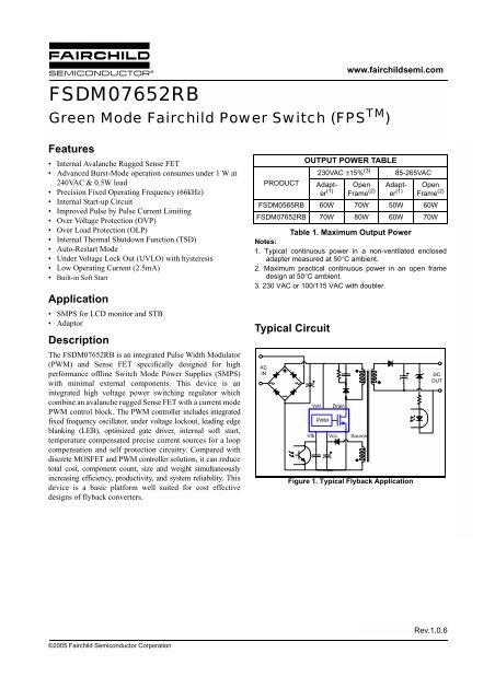
FSDM07652RB Green Mode Fairchild Power Switch ... - HEStore.hu
FSDM07652RB Green Mode Fairchild Power Switch ... - HEStore.hu
FSDM07652RB Green Mode Fairchild Power Switch ... - HEStore.hu

You also want an ePaper? Increase the reach of your titles
YUMPU automatically turns print PDFs into web optimized ePapers that Google loves.
<strong>FSDM07652RB</strong><br />
<strong>Green</strong> <strong>Mode</strong> <strong>Fairchild</strong> <strong>Power</strong> <strong>Switch</strong> (FPS TM )<br />
www.fairchildsemi.com<br />
Features<br />
• Internal Avalanche Rugged Sense FET<br />
• Advanced Burst-<strong>Mode</strong> operation consumes under 1 W at<br />
240VAC & 0.5W load<br />
• Precision Fixed Operating Frequency (66kHz)<br />
• Internal Start-up Circuit<br />
• Improved Pulse by Pulse Current Limiting<br />
• Over Voltage Protection (OVP)<br />
• Over Load Protection (OLP)<br />
• Internal Thermal S<strong>hu</strong>tdown Function (TSD)<br />
• Auto-Restart <strong>Mode</strong><br />
• Under Voltage Lock Out (UVLO) with hysteresis<br />
• Low Operating Current (2.5mA)<br />
• Built-in Soft Start<br />
Application<br />
• SMPS for LCD monitor and STB<br />
• Adaptor<br />
Description<br />
The <strong>FSDM07652RB</strong> is an integrated Pulse Width Modulator<br />
(PWM) and Sense FET specifically designed for high<br />
performance offline <strong>Switch</strong> <strong>Mode</strong> <strong>Power</strong> Supplies (SMPS)<br />
with minimal external components. This device is an<br />
integrated high voltage power switching regulator which<br />
combine an avalanche rugged Sense FET with a current mode<br />
PWM control block. The PWM controller includes integrated<br />
fixed frequency oscillator, under voltage lockout, leading edge<br />
blanking (LEB), optimized gate driver, internal soft start,<br />
temperature compensated precise current sources for a loop<br />
compensation and self protection circuitry. Compared with<br />
discrete MOSFET and PWM controller solution, it can reduce<br />
total cost, component count, size and weight simultaneously<br />
increasing efficiency, productivity, and system reliability. This<br />
device is a basic platform well suited for cost effective<br />
designs of flyback converters.<br />
OUTPUT POWER TABLE<br />
230VAC ±15% (3) 85-265VAC<br />
PRODUCT Adapter<br />
Open<br />
Frame (2)<br />
Adapter<br />
Open<br />
Frame (2)<br />
FSDM0565RB 60W 70W 50W 60W<br />
<strong>FSDM07652RB</strong> 70W 80W 60W 70W<br />
Table 1. Maximum Output <strong>Power</strong><br />
Notes:<br />
1. Typical continuous power in a non-ventilated enclosed<br />
adapter measured at 50°C ambient.<br />
2. Maximum practical continuous power in an open frame<br />
design at 50°C ambient.<br />
3. 230 VAC or 100/115 VAC with doubler.<br />
Typical Circuit<br />
AC<br />
IN<br />
Vfb<br />
Vstr<br />
PWM<br />
Drain<br />
Vcc<br />
Source<br />
Figure 1. Typical Flyback Application<br />
DC<br />
OUT<br />
Rev.1.0.6<br />
©2005 <strong>Fairchild</strong> Semiconductor Corporation
<strong>FSDM07652RB</strong><br />
Internal Block Diagram<br />
Vcc<br />
Vstr<br />
Drain<br />
3 6<br />
1<br />
N.C<br />
5<br />
I start<br />
0.5/0.7V<br />
+<br />
-<br />
8V/12V<br />
Vcc good<br />
Vref<br />
Internal<br />
Bias<br />
Vcc<br />
Vref<br />
FB 4<br />
I delay<br />
I FB<br />
Soft start<br />
2.5R<br />
PWM<br />
R<br />
OSC<br />
S<br />
R<br />
Q<br />
Q<br />
Gate<br />
driver<br />
LEB<br />
V SD<br />
Vcc<br />
Vovp<br />
TSD<br />
Vcc good<br />
S<br />
R<br />
Q<br />
Q<br />
V CL<br />
2<br />
GND<br />
Figure 2. Functional Block Diagram of <strong>FSDM07652RB</strong><br />
2
<strong>FSDM07652RB</strong><br />
Pin Definitions<br />
Pin Number Pin Name Pin Function Description<br />
1 Drain<br />
This pin is the high voltage power Sense FET drain. It is designed to drive the<br />
transformer directly.<br />
2 GND This pin is the control ground and the Sense FET source.<br />
3 Vcc<br />
This pin is the positive supply voltage input. During start up, the power is supplied<br />
by an internal high voltage current source that is connected to the Vstr pin.<br />
When Vcc reaches 12V, the internal high voltage current source is disabled and<br />
the power is supplied from the auxiliary transformer winding.<br />
4 Vfb<br />
This pin is internally connected to the inverting input of the PWM comparator.<br />
The collector of an opto-coupler is typically tied to this pin. For stable operation,<br />
a capacitor should be placed between this pin and GND. If the voltage of this pin<br />
reaches 6.0V, the over load protection is activated resulting in s<strong>hu</strong>tdown of the<br />
FPS TM .<br />
5 N.C -<br />
6 Vstr<br />
This pin is connected directly to the high voltage DC link. At startup, the internal<br />
high voltage current source supplies internal bias and charges the external capacitor<br />
that is connected to the Vcc pin. Once Vcc reaches 12V, the internal current<br />
source is disabled.<br />
Pin Configuration<br />
TO-220F-6L<br />
6.Vstr<br />
5.N.C.<br />
4.Vfb<br />
3.Vcc<br />
2.GND<br />
1.Drain<br />
Figure 3. Pin Configuration (Top View)<br />
3
<strong>FSDM07652RB</strong><br />
Absolute Maximum Ratings<br />
(Ta=25°C, unless otherwise specified)<br />
Parameter Symbol Value Unit<br />
Drain-source voltage VBSS 650 V<br />
Vstr Max Voltage VSTR 650 V<br />
Pulsed Drain current (Tc=25°C) (1) IDM 15 ADC<br />
Continuous Drain Current(Tc=25°C)<br />
3.8 A<br />
ID<br />
Continuous Drain Current(Tc=100°C) 2.4 A<br />
Single pulsed avalanche energy (2) EAS 370 mJ<br />
Single pulsed avalanche current (3) IAS - A<br />
Supply voltage VCC 20 V<br />
Input voltage range VFB -0.3 to VCC V<br />
Total power dissipation(Tc=25°C) PD(Watt H/S) 45 W<br />
Operating junction temperature Tj Internally limited °C<br />
Operating ambient temperature TA -25 to +85 °C<br />
Storage temperature range TSTG -55 to +150 °C<br />
ESD Capability, HBM <strong>Mode</strong>l (All pins<br />
excepts for Vstr and Vfb)<br />
ESD Capability, Machine <strong>Mode</strong>l (All pins<br />
excepts for Vstr and Vfb)<br />
Notes:<br />
1. Repetitive rating: Pulse width limited by maximum junction temperature<br />
2. L=14mH, starting Tj=25°C<br />
3. L=13uH, starting Tj=25°C<br />
- 2.0<br />
(GND-Vstr/Vfb=1.5kV)<br />
- 300<br />
(GND-Vstr/Vfb=225V)<br />
kV<br />
V<br />
Thermal Impedance<br />
Parameter Symbol Value Unit<br />
Junction-to-Ambient Thermal θJA (1) 49.90 °C/W<br />
Junction-to-Case Thermal θJC (2) 2.78 °C/W<br />
Notes:<br />
1. Free standing with no heat-sink under natural convection.<br />
2. Infinite cooling condition - Refer to the SEMI G30-88.<br />
4
<strong>FSDM07652RB</strong><br />
Electrical Characteristics<br />
(Ta = 25°C unless otherwise specified)<br />
Parameter Symbol Condition Min. Typ. Max. Unit<br />
Sense FET SECTION<br />
Drain source breakdown voltage BVDSS VGS = 0V, ID = 250µA 650 - - V<br />
Zero gate voltage drain current<br />
IDSS<br />
VDS = 650V, VGS = 0V - - 500 µA<br />
VDS= 520V<br />
VGS = 0V, TC = 125°C<br />
- - 500 µA<br />
Static drain source on resistance (1) RDS(ON) VGS = 10V, ID = 2.5A - 1.4 1.6 Ω<br />
Output capacitance<br />
COSS<br />
VGS = 0V, VDS = 25V,<br />
f = 1MHz<br />
- 100 - pF<br />
Turn on delay time<br />
Rise time<br />
Turn off delay time<br />
TD(ON)<br />
TR<br />
TD(OFF)<br />
VDD= 325V, ID= 5A<br />
(MOSFET switching<br />
time is essentially<br />
independent of<br />
operating temperature)<br />
-<br />
-<br />
-<br />
22<br />
60<br />
115<br />
-<br />
-<br />
-<br />
Fall time TF - 65 -<br />
ns<br />
CONTROL SECTION<br />
Initial frequency FOSC VFB = 3V 60 66 72 kHz<br />
Voltage stability FSTABLE 13V ≤ Vcc ≤ 18V 0 1 3 %<br />
Temperature stability (2) ∆FOSC -25°C ≤ Ta ≤ 85°C 0 ±5 ±10 %<br />
Maximum duty cycle DMAX - 75 80 85 %<br />
Minimum duty cycle DMIN - - - 0 %<br />
Start threshold voltage VSTART VFB=GND 11 12 13 V<br />
Stop threshold voltage VSTOP VFB=GND 7 8 9 V<br />
Feedback source current IFB VFB=GND 0.7 0.9 1.1 mA<br />
Soft-start time TS Vfb=3 - 10 15 ms<br />
Leading Edge Blanking time TLEB - - 250 - ns<br />
BURST MODE SECTION<br />
Burst <strong>Mode</strong> Voltages (2) VBURH Vcc=14V - 0.7 - V<br />
VBURL Vcc=14V - 0.5 - V<br />
PROTECTION SECTION<br />
Peak current limit (4) IOVER VFB=5V, VCC=14V 2.2 2.5 2.8 A<br />
Over voltage protection VOVP - 18 19 20 V<br />
Thermal s<strong>hu</strong>tdown temperature (2) TSD 130 145 160 °C<br />
S<strong>hu</strong>tdown feedback voltage VSD VFB ≥ 5.5V 5.5 6.0 6.5 V<br />
S<strong>hu</strong>tdown delay current IDELAY VFB=5V 2.8 3.5 4.2 µA<br />
5
<strong>FSDM07652RB</strong><br />
TOTAL DEVICE SECTION<br />
Operating supply current (5) IOP(MIN) VFB=GND, VCC=10V<br />
IOP VFB=GND, VCC=14V<br />
- 2.5 5 mA<br />
IOP(MAX)<br />
VFB=GND, VCC=18V<br />
Notes:<br />
1. Pulse test : Pulse width ≤ 300µS, duty ≤ 2%<br />
2. These parameters, although guaranteed at the design, are not tested in mass production.<br />
3. These parameters, although guaranteed, are tested only in EDS(wafer test) process.<br />
4. These parameters indicate the inductor current.<br />
5. This parameter is the current flowing into the control IC.<br />
6
<strong>FSDM07652RB</strong><br />
Comparison Between FS6M07652RTC and <strong>FSDM07652RB</strong><br />
Function FS6M07652RTC <strong>FSDM07652RB</strong> <strong>FSDM07652RB</strong> Advantages<br />
Soft-Start<br />
Adjustable soft-start Internal soft-start with • Gradually increasing current limit<br />
time using an<br />
external capacitor<br />
typically 10ms (fixed) during soft-start further reduces peak<br />
current and voltage component<br />
stresses<br />
• Eliminates external components used<br />
for soft-start in most applications<br />
• Reduces or eliminates output<br />
overshoot<br />
Burst <strong>Mode</strong> Operation<br />
• Built into controller<br />
• Output voltage<br />
drops to around<br />
half<br />
• Built into controller • Improve light load efficiency<br />
• Output voltage fixed • Reduces no-load consumption<br />
7
<strong>FSDM07652RB</strong><br />
Typical Performance Characteristics<br />
(These Characteristic Graphs are Normalized at Ta= 25°C)<br />
Operating Current<br />
(Normalized to 25℃)<br />
1.2<br />
1.0<br />
0.8<br />
0.6<br />
0.4<br />
0.2<br />
0.0<br />
-50 -25 0 25 50 75 100 125<br />
Junction Temperature(℃)<br />
Operating Current vs. Temp<br />
Start Thershold Voltage<br />
(Normalized to 25℃)<br />
1.2<br />
1.0<br />
0.8<br />
0.6<br />
0.4<br />
0.2<br />
0.0<br />
-50 -25 0 25 50 75 100 125<br />
Junction Temperature(℃)<br />
Start Threshold Voltage vs. Temp<br />
Stop Threshold Voltage<br />
(Normalized to 25℃)<br />
1.2<br />
1.0<br />
0.8<br />
0.6<br />
0.4<br />
0.2<br />
0.0<br />
-50 -25 0 25 50 75 100 125<br />
Junction Temperature(℃)<br />
Stop Threshold Voltage vs. Temp<br />
Initial Frequency<br />
(Normalized to 25℃)<br />
1.2<br />
1.0<br />
0.8<br />
0.6<br />
0.4<br />
0.2<br />
0.0<br />
-50 -25 0 25 50 75 100 125<br />
Junction Temperature(℃)<br />
Operating Freqency vs. Temp<br />
1.2<br />
1.0<br />
1.2<br />
1.0<br />
Maximum Duty Cycle<br />
(Normalized to 25℃)<br />
0.8<br />
0.6<br />
0.4<br />
0.2<br />
FB Source Current<br />
(Normalized to 25℃)<br />
0.8<br />
0.6<br />
0.4<br />
0.2<br />
0.0<br />
-50 -25 0 25 50 75 100 125<br />
Junction Temperature(℃)<br />
0.0<br />
-50 -25 0 25 50 75 100 125<br />
Junction Temperature(℃)<br />
Maximum Duty vs. Temp<br />
Feedback Source Current vs. Temp<br />
8
<strong>FSDM07652RB</strong><br />
Typical Performance Characteristics (Continued)<br />
(These Characteristic Graphs are Normalized at Ta= 25°C)<br />
1.2<br />
1.2<br />
1.0<br />
1.0<br />
S<strong>hu</strong>tdown FB Voltage<br />
(Normalized to 25℃)<br />
0.8<br />
0.6<br />
0.4<br />
0.2<br />
S<strong>hu</strong>tdown Delay Current<br />
(Normalized to 25℃)<br />
0.8<br />
0.6<br />
0.4<br />
0.2<br />
0.0<br />
-50 -25 0 25 50 75 100 125<br />
Junction Temperature(℃)<br />
0.0<br />
-50 -25 0 25 50 75 100 125<br />
Junction Temperature(℃)<br />
S<strong>hu</strong>tDown Feedback Voltage vs. Temp<br />
S<strong>hu</strong>tDown Delay Current vs. Temp<br />
Over Voltage Protection<br />
(Normalized to 25℃)<br />
1.2<br />
1.0<br />
0.8<br />
0.6<br />
0.4<br />
0.2<br />
0.0<br />
-50 -25 0 25 50 75 100 125<br />
Junction Temperature(℃)<br />
Over Voltage Protection vs. Temp<br />
Burst <strong>Mode</strong> Enable Voltage<br />
(Normalized to 25℃)<br />
1.2<br />
1.0<br />
0.8<br />
0.6<br />
0.4<br />
0.2<br />
0.0<br />
-50 -25 0 25 50 75 100 125<br />
Junction Temperature(℃)<br />
Burst <strong>Mode</strong> Enable Voltage vs. Temp<br />
Burst <strong>Mode</strong> Disable Voltage<br />
(Normalized to 25℃)<br />
1.2<br />
1.0<br />
0.8<br />
0.6<br />
0.4<br />
0.2<br />
0.0<br />
-50 -25 0 25 50 75 100 125<br />
Junction Temperature(℃)<br />
Over Current Limit<br />
(Normalized to 25℃)<br />
1.2<br />
1.0<br />
0.8<br />
0.6<br />
0.4<br />
0.2<br />
0.0<br />
-50 -25 0 25 50 75 100 125<br />
Junction Temperature(℃)<br />
Burst <strong>Mode</strong> Disable Voltage vs. Temp<br />
Current Limit vs. Temp<br />
9
<strong>FSDM07652RB</strong><br />
Typical Performance Characteristics (Continued)<br />
(These Characteristic Graphs are Normalized at Ta= 25°C)<br />
1.2<br />
1.0<br />
Soft Start Time<br />
(Normalized to 25℃)<br />
0.8<br />
0.6<br />
0.4<br />
0.2<br />
0.0<br />
-50 -25 0 25 50 75 100 125<br />
Junction Temperature(℃)<br />
Soft Start Time vs. Temp<br />
10
<strong>FSDM07652RB</strong><br />
Functional Description<br />
1. Startup : In previous generations of <strong>Fairchild</strong> <strong>Power</strong><br />
<strong>Switch</strong>es (FPS TM ) the Vcc pin had an external start-up<br />
resistor to the DC input voltage line. In this generation the<br />
startup resistor is replaced by an internal high voltage current<br />
source. At startup, an internal high voltage current source<br />
supplies the internal bias and charges the external capacitor<br />
(Cvcc) that is connected to the Vcc pin as illustrated in<br />
Figure 4. When Vcc reaches 12V, the <strong>FSDM07652RB</strong><br />
begins switching and the internal high voltage current source<br />
is disabled. Then, the <strong>FSDM07652RB</strong> continues its normal<br />
switching operation and the power is supplied from the<br />
auxiliary transformer winding unless Vcc goes below the<br />
stop voltage of 8V.<br />
V DC<br />
2.1 Pulse-by-pulse current limit: Because current mode<br />
control is employed, the peak current through the Sense FET<br />
is limited by the inverting input of PWM comparator (Vfb*)<br />
as shown in Figure 5. Assuming that the 0.9mA current<br />
source flows only through the internal resistor (2.5R +R= 2.8<br />
kΩ), the cathode voltage of diode D2 is about 2.5V. Since D1<br />
is blocked when the feedback voltage (Vfb) exceeds 2.5V,<br />
the maximum voltage of the cathode of D2 is clamped at this<br />
voltage, t<strong>hu</strong>s clamping Vfb*. Therefore, the peak value of<br />
the current through the Sense FET is limited.<br />
2.2 Leading edge blanking (LEB) : At the instant the<br />
internal Sense FET is turned on, there usually exists a high<br />
current spike through the Sense FET, caused by primary-side<br />
capacitance and secondary-side rectifier reverse recovery.<br />
Excessive voltage across the Rsense resistor would lead to<br />
incorrect feedback operation in the current mode PWM<br />
control. To counter this effect, the <strong>FSDM07652RB</strong> employs<br />
a leading edge blanking (LEB) circuit. This circuit inhibits<br />
the PWM comparator for a short time (TLEB) after the Sense<br />
FET is turned on.<br />
3<br />
Vcc<br />
6 Vstr<br />
I start<br />
I delay<br />
I FB<br />
Vcc<br />
Vref<br />
8V/12V<br />
Vcc good<br />
Vref<br />
Vo<br />
C Vcc<br />
4 OSC<br />
Vfb<br />
H11A817A<br />
C B<br />
D1<br />
D2<br />
2.5R<br />
SenseFET<br />
Internal<br />
Bias<br />
KA431<br />
+<br />
V fb *<br />
-<br />
R<br />
Gate<br />
driver<br />
Figure 4. Internal startup circuit<br />
V SD<br />
OLP<br />
R sense<br />
Figure 5. Pulse width modulation (PWM) circuit<br />
2. Feedback Control : <strong>FSDM07652RB</strong> employs current<br />
mode control, as shown in Figure 5. An opto-coupler (such<br />
as the H11A817A) and s<strong>hu</strong>nt regulator (such as the KA431)<br />
are typically used to implement the feedback network.<br />
Comparing the feedback voltage with the voltage across the<br />
Rsense resistor plus an offset voltage makes it possible to<br />
control the switching duty cycle. When the reference pin<br />
voltage of the KA431 exceeds the internal reference voltage<br />
of 2.5V, the H11A817A LED current increases, t<strong>hu</strong>s pulling<br />
down the feedback voltage and reducing the duty cycle. This<br />
event typically happens when the input voltage is increased<br />
or the output load is decreased.<br />
3. Protection Circuit : The <strong>FSDM07652RB</strong> has several self<br />
protective functions such as over load protection (OLP), over<br />
voltage protection (OVP) and thermal s<strong>hu</strong>tdown (TSD).<br />
Because these protection circuits are fully integrated into the<br />
IC without external components, the reliability can be<br />
improved without increasing cost. Once the fault condition<br />
occurs, switching is terminated and the Sense FET remains<br />
off. This causes Vcc to fall. When Vcc reaches the UVLO<br />
stop voltage, 8V, the protection is reset and the internal high<br />
voltage current source charges the Vcc capacitor via the Vstr<br />
pin. When Vcc reaches the UVLO start voltage,12V, the<br />
<strong>FSDM07652RB</strong> resumes its normal operation. In this<br />
manner, the auto-restart can alternately enable and disable<br />
the switching of the power Sense FET until the fault<br />
condition is eliminated (see Figure 6).<br />
11
<strong>FSDM07652RB</strong><br />
Vds<br />
<strong>Power</strong><br />
on<br />
Fault<br />
occurs<br />
Fault<br />
removed<br />
V FB<br />
6.0V<br />
Over load protection<br />
2.5V<br />
Vcc<br />
T 12<br />
12<br />
= Cfb*(6.0-2.5)/I delay<br />
delay<br />
12V<br />
8V<br />
T 1<br />
T 2<br />
Figure 7. Over load protection<br />
t<br />
Normal<br />
operation<br />
Fault<br />
situation<br />
Figure 6. Auto restart operation<br />
Normal<br />
operation<br />
3.1 Over Load Protection (OLP) : Overload is defined as<br />
the load current exceeding a pre-set level due to an<br />
unexpected event. In this situation, the protection circuit<br />
should be activated in order to protect the SMPS. However,<br />
even when the SMPS is in the normal operation, the over<br />
load protection circuit can be activated during the load<br />
transition. In order to avoid this undesired operation, the over<br />
load protection circuit is designed to be activated after a<br />
specified time to determine whether it is a transient situation<br />
or an overload situation. Because of the pulse-by-pulse<br />
current limit capability, the maximum peak current through<br />
the Sense FET is limited, and therefore the maximum input<br />
power is restricted with a given input voltage. If the output<br />
consumes beyond this maximum power, the output voltage<br />
(Vo) decreases below the set voltage. This reduces the<br />
current through the opto-coupler LED, which also reduces<br />
the opto-coupler transistor current, t<strong>hu</strong>s increasing the<br />
feedback voltage (Vfb). If Vfb exceeds 2.5V, D1 is blocked<br />
and the 3.5uA current source starts to charge CB slowly up to<br />
Vcc. In this condition, Vfb continues increasing until it<br />
reaches 6V, when the switching operation is terminated as<br />
shown in Figure 7. The delay time for s<strong>hu</strong>tdown is the time<br />
required to charge CB from 2.5V to 6.0V with 3.5uA. In<br />
general, a 10 ~ 50 ms delay time is typical for most<br />
applications.<br />
t<br />
3.2 Over voltage Protection (OVP) : If the secondary side<br />
feedback circuit were to malfunction or a solder defect<br />
caused an open in the feedback path, the current through the<br />
opto-coupler transistor becomes almost zero. Then, Vfb<br />
climbs up in a similar manner to the over load situation,<br />
forcing the preset maximum current to be supplied to the<br />
SMPS until the over load protection is activated. Because<br />
more energy than required is provided to the output, the<br />
output voltage may exceed the rated voltage before the over<br />
load protection is activated, resulting in the breakdown of the<br />
devices in the secondary side. In order to prevent this<br />
situation, an over voltage protection (OVP) circuit is<br />
employed. In general, Vcc is proportional to the output<br />
voltage and the <strong>FSDM07652RB</strong> uses Vcc instead of directly<br />
monitoring the output voltage. If VCC exceeds 19V, an OVP<br />
circuit is activated resulting in the termination of the<br />
switching operation. In order to avoid undesired activation of<br />
OVP during normal operation, Vcc should be designed to be<br />
below 19V.<br />
3.3 Thermal S<strong>hu</strong>tdown (TSD) : The Sense FET and the<br />
control IC are built in one package. This makes it easy for<br />
the control IC to detect the heat generation from the Sense<br />
FET. When the temperature exceeds approximately 150°C,<br />
the thermal s<strong>hu</strong>tdown is activated.<br />
4. Soft Start : The <strong>FSDM07652RB</strong> has an internal soft start<br />
circuit that increases PWM comparator inverting input<br />
voltage together with the Sense FET current slowly after it<br />
starts up. The typical soft start time is 10msec, The pulse<br />
width to the power switching device is progressively<br />
increased to establish the correct working conditions for<br />
transformers, inductors, and capacitors. The voltage on the<br />
output capacitors is progressively increased with the<br />
intention of smoothly establishing the required output<br />
voltage. It also helps to prevent transformer saturation and<br />
reduce the stress on the secondary diode during startup.<br />
12
<strong>FSDM07652RB</strong><br />
5. Burst operation : In order to minimize power dissipation<br />
in standby mode, the <strong>FSDM07652RB</strong> enters burst mode<br />
operation. As the load decreases, the feedback voltage<br />
decreases. As shown in Figure 8, the device automatically<br />
enters burst mode when the feedback voltage drops below<br />
VBURL(500mV). At this point switching stops and the<br />
output voltages start to drop at a rate dependent on standby<br />
current load. This causes the feedback voltage to rise. Once<br />
it passes VBURH(700mV) switching resumes. The feedback<br />
voltage then falls and the process repeats. Burst mode<br />
operation alternately enables and disables switching of the<br />
power Sense FET thereby reducing switching loss in<br />
Standby mode.<br />
Vo<br />
Vo set<br />
V FB<br />
0.7V<br />
0.5V<br />
Ids<br />
Vds<br />
<strong>Switch</strong>ing<br />
disabled<br />
<strong>Switch</strong>ing<br />
disabled<br />
T1<br />
T2 T3<br />
T4<br />
Figure 8. Waveforms of burst operation<br />
time<br />
13
<strong>FSDM07652RB</strong><br />
Typical application circuit<br />
Application Output power Input voltage Output voltage (Max current)<br />
LCD Monitor<br />
40W<br />
Universal input<br />
(85-265Vac)<br />
Features<br />
• High efficiency (>81% at 85Vac input)<br />
• Low zero load power consumption (
<strong>FSDM07652RB</strong><br />
2. Transformer Schematic Diagram<br />
EER3016<br />
1<br />
10<br />
N p<br />
/2<br />
2<br />
9<br />
N p<br />
/2<br />
3<br />
8<br />
4<br />
7<br />
N 5 6<br />
a<br />
N 12V<br />
N 5V<br />
3.Winding Specification<br />
No Pin (s→f) Wire Turns Winding Method<br />
Na 4 → 5 0.2 φ × 1 8 Center Winding<br />
Insulation: Polyester Tape t = 0.050mm, 2Layers<br />
Np/2 2 → 1 0.4 φ × 1 18 Solenoid Winding<br />
Insulation: Polyester Tape t = 0.050mm, 2Layers<br />
N12V 10 → 8 0.3 φ × 3 7 Center Winding<br />
Insulation: Polyester Tape t = 0.050mm, 2Layers<br />
N5V 7 → 6 0.3 φ × 3 3 Center Winding<br />
Insulation: Polyester Tape t = 0.050mm, 2Layers<br />
Np/2 3 → 2 0.4 φ × 1 18 Solenoid Winding<br />
Outer Insulation: Polyester Tape t = 0.050mm, 2Layers<br />
4.Electrical Characteristics<br />
Pin Specification Remarks<br />
Inductance 1 - 3 520uH ± 10% 100kHz, 1V<br />
Leakage Inductance 1 - 3 10uH Max 2 nd all short<br />
5. Core & Bobbin<br />
Core : EER 3016<br />
Bobbin : EER3016<br />
Ae(mm2) : 96<br />
15
<strong>FSDM07652RB</strong><br />
6.Demo Circuit Part List<br />
Part Value Note Part Value Note<br />
Fuse C301 4.7nF Polyester Film Cap.<br />
F101 2A/250V<br />
NTC<br />
Inductor<br />
RT101 5D-9 L201 5uH Wire 1.2mm<br />
Resistor L202 5uH Wire 1.2mm<br />
R101 560K 1W<br />
R102 30K 1/4W<br />
R103 56K 2W<br />
R104 5 1/4W Diode<br />
R105 40K 1/4W D101 UF4007<br />
R201 1K 1/4W D102 TVR10G<br />
R202 1.2K 1/4W D201 MBRF1045<br />
R203 12K 1/4W D202 MBRF10100<br />
R204 5.6K 1/4W ZD101 Zener Diode 22V<br />
R205 5.6K 1/4W ZD102 Zener Diode 10V<br />
Bridge Diode<br />
BD101 2KBP06M 3N257 Bridge Diode<br />
Capacitor<br />
C101 220nF/275VAC Box Capacitor Line Filter<br />
C102 220nF/275VAC Box Capacitor LF101 23mH Wire 0.4mm<br />
C103 100uF/400V Electrolytic Capacitor IC<br />
C104 2.2nF/1kV Ceramic Capacitor IC101 <strong>FSDM07652RB</strong> FPS TM (5A,650V)<br />
C105 22uF/50V Electrolytic Capacitor IC201 KA431(TL431) Voltage reference<br />
C106 47nF/50V Ceramic Capacitor IC301 H11A817A Opto-coupler<br />
C201 1000uF/25V Electrolytic Capacitor<br />
C202 1000uF/25V Electrolytic Capacitor<br />
C203 1000uF/10V Electrolytic Capacitor<br />
C204 1000uF/10V Electrolytic Capacitor<br />
C205 47nF/50V Ceramic Capacitor<br />
16
<strong>FSDM07652RB</strong><br />
7. Layout<br />
Figure 9. Layout Considerations for <strong>FSDM07652RB</strong><br />
Figure 10. Layout Considerations for <strong>FSDM07652RB</strong><br />
17
<strong>FSDM07652RB</strong><br />
Package Dimensions<br />
TO-220F-6L(Forming)<br />
18
<strong>FSDM07652RB</strong><br />
Ordering Information<br />
Product Number Package Marking Code BVdss Rds(on)Max.<br />
<strong>FSDM07652RB</strong>WDTU TO-220F-6L(Forming) DM07652R 650V 1.6 Ω<br />
WDTU : Forming Type<br />
19
<strong>FSDM07652RB</strong><br />
DISCLAIMER<br />
FAIRCHILD SEMICONDUCTOR RESERVES THE RIGHT TO MAKE CHANGES WITHOUT FURTHER NOTICE TO ANY<br />
PRODUCTS HEREIN TO IMPROVE RELIABILITY, FUNCTION OR DESIGN. FAIRCHILD DOES NOT ASSUME ANY<br />
LIABILITY ARISING OUT OF THE APPLICATION OR USE OF ANY PRODUCT OR CIRCUIT DESCRIBED HEREIN; NEITHER<br />
DOES IT CONVEY ANY LICENSE UNDER ITS PATENT RIGHTS, NOR THE RIGHTS OF OTHERS.<br />
LIFE SUPPORT POLICY<br />
FAIRCHILD’S PRODUCTS ARE NOT AUTHORIZED FOR USE AS CRITICAL COMPONENTS IN LIFE SUPPORT DEVICES<br />
OR SYSTEMS WITHOUT THE EXPRESS WRITTEN APPROVAL OF THE PRESIDENT OF FAIRCHILD SEMICONDUCTOR<br />
CORPORATION. As used herein:<br />
1. Life support devices or systems are devices or systems<br />
which, (a) are intended for surgical implant into the body,<br />
or (b) support or sustain life, and (c) whose failure to<br />
perform when properly used in accordance with<br />
instructions for use provided in the labeling, can be<br />
reasonably expected to result in a significant injury of the<br />
user.<br />
2. A critical component in any component of a life support<br />
device or system whose failure to perform can be<br />
reasonably expected to cause the failure of the life support<br />
device or system, or to affect its safety or effectiveness.<br />
www.fairchildsemi.com<br />
1/12/05 0.0m 001<br />
© 2005 <strong>Fairchild</strong> Semiconductor Corporation


