

BF961 NâChannel Dual Gate MOS-Fieldeffect Tetrode, Depletion ...
BF961 NâChannel Dual Gate MOS-Fieldeffect Tetrode, Depletion ...
BF961 NâChannel Dual Gate MOS-Fieldeffect Tetrode, Depletion ...

Create successful ePaper yourself
Turn your PDF publications into a flip-book with our unique Google optimized e-Paper software.
N–Channel <strong>Dual</strong> <strong>Gate</strong> <strong>MOS</strong>-<strong>Fieldeffect</strong> <strong>Tetrode</strong>,<br />
<strong>Depletion</strong> Mode<br />
Electrostatic sensitive device.<br />
Observe precautions for handling.<br />
<strong>BF961</strong><br />
Vishay Semiconductors<br />
Applications<br />
Input- and mixer stages especially for FM- and VHF TV-tuners up to 300 MHz.<br />
Features<br />
<br />
<br />
<br />
Integrated gate protection diodes<br />
High cross modulation performance<br />
Low noise figure<br />
<br />
<br />
<br />
High AGC-range<br />
Low feedback capacitance<br />
Low input capacitance<br />
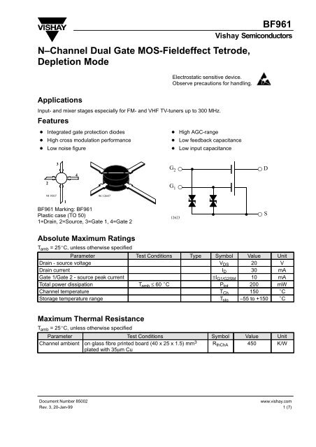
3<br />
4<br />
G 2<br />
D<br />
2<br />
G 1<br />
94 9307 96 12647<br />
1<br />
<strong>BF961</strong> Marking: <strong>BF961</strong><br />
Plastic case (TO 50)<br />
1=Drain, 2=Source, 3=<strong>Gate</strong> 1, 4=<strong>Gate</strong> 2<br />
12623<br />
S<br />
Absolute Maximum Ratings<br />
T amb = 25 C, unless otherwise specified<br />
Parameter Test Conditions Type Symbol Value Unit<br />
Drain - source voltage V DS 20 V<br />
Drain current I D 30 mA<br />
<strong>Gate</strong> 1/<strong>Gate</strong> 2 - source peak current ±I G1/G2SM 10 mA<br />
Total power dissipation T amb ≤ 60 C P tot 200 mW<br />
Channel temperature T Ch 150 C<br />
Storage temperature range T stg –55 to +150 C<br />
Maximum Thermal Resistance<br />
T amb = 25 C, unless otherwise specified<br />
Parameter Test Conditions Symbol Value Unit<br />
Channel ambient on glass fibre printed board (40 x 25 x 1.5) mm 3<br />
plated with 35m Cu<br />
R thChA 450 K/W<br />
Document Number 85002<br />
www.vishay.com<br />
Rev. 3, 20-Jan-99 1 (7)
<strong>BF961</strong><br />
Vishay Semiconductors<br />
Electrical DC Characteristics<br />
T amb = 25 C, unless otherwise specified<br />
Parameter Test Conditions Type Symbol Min Typ Max Unit<br />
Drain - source I D = 10 A, –V G1S = –V G2S = 4 V V (BR)DS 20 V<br />
breakdown voltage<br />
<strong>Gate</strong> 1 - source ±I G1S = 10 mA, V G2S = V DS = 0 ±V (BR)G1SS 8 14 V<br />
breakdown voltage<br />
<strong>Gate</strong> 2 - source ±I G2S = 10 mA, V G1S = V DS = 0 ±V (BR)G2SS 8 14 V<br />
breakdown voltage<br />
<strong>Gate</strong> 1 - source ±V G1S = 5 V, V G2S = V DS = 0 ±I G1SS 100 nA<br />
leakage current<br />
<strong>Gate</strong> 2 - source ±V G2S = 5 V, V G1S = V DS = 0 ±I G2SS 100 nA<br />
leakage current<br />
Drain current V DS = 15 V, V G1S = 0, V G2S = 4 V <strong>BF961</strong> I DSS 4 20 mA<br />
<strong>BF961</strong>A I DSS 4 10.5 mA<br />
<strong>BF961</strong>B I DSS 9.5 20 mA<br />
<strong>Gate</strong> 1 - source V DS = 15 V, V G2S = 4 V, I D = 20 A –V G1S(OFF) 3.5 V<br />
cut-off voltage<br />
<strong>Gate</strong> 2 - source<br />
cut-off voltage<br />
V DS = 15 V, V G1S = 0, I D = 20 A –V G2S(OFF) 3.5 V<br />
Electrical AC Characteristics<br />
V DS = 15 V, I D = 10 mA, V G2S = 4 V, f = 1 MHz , T amb = 25 C, unless otherwise specified<br />
Parameter Test Conditions Symbol Min Typ Max Unit<br />
Forward transadmittance ⏐y 21s ⏐ 12 15 mS<br />
<strong>Gate</strong> 1 input capacitance C issg1 3.7 pF<br />
<strong>Gate</strong> 2 input capacitance V G1S = 0, V G2S = 4 V C issg2 1.6 pF<br />
Feedback capacitance C rss 25 fF<br />
Output capacitance C oss 1.6 pF<br />
Power gain G S = 2 mS, G L = 0.5 mS, f = 200 MHz G ps 20 dB<br />
AGC range V G2S = 4 to –2 V, f = 200 MHz G ps 50 dB<br />
Noise figure G S = 2 mS, G L = 0.5 mS, f = 200 MHz F 1.8 2.5 dB<br />
www.vishay.com<br />
2 (7)<br />
Document Number 85002<br />
Rev. 3, 20-Jan-99
Typical Characteristics (T amb = 25 C unless otherwise specified)<br />
<strong>BF961</strong><br />
Vishay Semiconductors<br />
P tot – Total Power Dissipation ( mW )<br />
96 12159<br />
I D – Drain Current ( mA )<br />
96 12160<br />
Y 21S – Forward Transadmittance ( mS )<br />
300<br />
250<br />
200<br />
150<br />
100<br />
50<br />
0<br />
0 20 40 60 80 100 120 140 160<br />
22<br />
20<br />
18<br />
16<br />
14<br />
12<br />
10<br />
T amb – Ambient Temperature ( °C )<br />
Figure 1. Total Power Dissipation vs.<br />
Ambient Temperature<br />
V G1S = 0.6V<br />
0.4V<br />
0.2V<br />
8<br />
–0.2V<br />
6<br />
–0.4V<br />
4<br />
–0.6V<br />
2<br />
–0.8V<br />
0<br />
0 2 4 6 8 10 12 14 16 18 20 22 24<br />
V DS – Drain Source Voltage ( V )<br />
Figure 2. Drain Current vs. Drain Source Voltage<br />
96 12161<br />
24<br />
22<br />
20<br />
18<br />
16<br />
14<br />
12<br />
10<br />
8<br />
6<br />
4<br />
2<br />
0<br />
V DS =15V<br />
I DS =10mA<br />
–2 –1 0 1 2 3 4 5 6<br />
V G2S – <strong>Gate</strong> 2 Source Voltage ( V )<br />
0<br />
V G1S =0.5V<br />
0V<br />
–0.5V<br />
Figure 3. Forward Transadmittance vs.<br />
<strong>Gate</strong> 2 Source Voltage<br />
Y 21S – Forward Transadmittance ( mS )<br />
96 12162<br />
C issg1 – <strong>Gate</strong> 1 Input Capacitance ( pF )<br />
96 12163<br />
C issg2 – <strong>Gate</strong> 2 Input Capacitance ( pF )<br />
96 12164<br />
22<br />
20<br />
18<br />
16<br />
14<br />
12<br />
10<br />
4.0<br />
3.5<br />
3.0<br />
2.5<br />
2.0<br />
1.5<br />
1.0<br />
0.5<br />
V DS =15V<br />
f=1MHz V G2S =5V<br />
8<br />
4V<br />
6<br />
4<br />
0V<br />
3V<br />
2<br />
2V<br />
1V<br />
0<br />
–2.0–1.5–1.0–0.5 0.0 0.5 1.0 1.5 2.0 2.5 3.0 3.5<br />
V G1S – <strong>Gate</strong> 1 Source Voltage ( V )<br />
Figure 4. Forward Transadmittance vs.<br />
<strong>Gate</strong> 1 Source Voltage<br />
V DS =15V<br />
V G2S =4V<br />
f=1MHz<br />
0<br />
–2.0 –1.5 –1.0 –0.5 0.0 0.5 1.0 1.5 2.0 2.5 3.0<br />
4.0<br />
3.6<br />
3.2<br />
2.8<br />
2.4<br />
2.0<br />
1.6<br />
1.2<br />
0.8<br />
0.4<br />
V G1S – <strong>Gate</strong> 1 Source Voltage ( V )<br />
Figure 5. <strong>Gate</strong> 1 Input Capacitance vs.<br />
<strong>Gate</strong> 1 Source Voltage<br />
V DS =15V<br />
V G1S =0<br />
f=1MHz<br />
0<br />
–2 –1 0 1 2 3 4 5 6 7<br />
V G2S – <strong>Gate</strong> 2 Source Voltage ( V )<br />
Figure 6. <strong>Gate</strong> 2 Input Capacitance vs.<br />
<strong>Gate</strong> 2 Source Voltage<br />
Document Number 85002<br />
www.vishay.com<br />
Rev. 3, 20-Jan-99 3 (7)
<strong>BF961</strong><br />
Vishay Semiconductors<br />
C oss – Output Capacitance ( pF )<br />
96 12165<br />
3.0<br />
2.5<br />
2.0<br />
1.5<br />
1.0<br />
0.5<br />
V G2S =4V<br />
f=1MHz<br />
0<br />
0 2 4 6 8 10 12 14 16 18 20 22<br />
V DS – Drain Source Voltage ( V )<br />
Figure 7. Output Capacitance vs. Drain Source Voltage<br />
Im ( y 11 ) ( mS )<br />
96 12166<br />
18<br />
16<br />
14<br />
12<br />
10<br />
8<br />
6<br />
4<br />
2<br />
600MHz<br />
300MHz<br />
200MHz<br />
100MHz<br />
400MHz<br />
f=700MHz<br />
500MHz<br />
0<br />
0 1 2 3 4 5 6 7 8 9 10<br />
Re (y 11 ) ( mS )<br />
V DS =15V<br />
V G2S =4V<br />
I D =5...20mA<br />
f=50...700MHz<br />
Figure 8. Short Circuit Input Admittance<br />
Im ( y 21 ) ( mS )<br />
96 12167<br />
10<br />
5<br />
0<br />
V DS =15V<br />
V G2S =4V<br />
f=50...700MHz<br />
–5<br />
I D =5mA<br />
100MHz<br />
10mA<br />
–10 20mA<br />
200MHz<br />
300MHz<br />
–15<br />
400MHz<br />
–20<br />
500MHz<br />
–25<br />
600MHz<br />
700MHz<br />
–30<br />
0 2 4 6 8 10 12 14 16 18 20 22 24 26 28<br />
Re (y 21 ) ( mS )<br />
f=50MHz<br />
Figure 9. Short Circuit Forward Transfer Admittance<br />
Im ( y 22 ) ( mS )<br />
96 12168<br />
7.0<br />
6.5<br />
6.0<br />
5.5<br />
5.0<br />
4.5<br />
4.0<br />
3.5<br />
3.0<br />
2.5<br />
2.0<br />
1.5<br />
1.0<br />
0.5<br />
0<br />
I D =5mA<br />
300MHz<br />
200MHz<br />
100MHz<br />
400MHz<br />
500MHz<br />
0 0.2 0.4 0.6 0.8 1.0 1.2 1.4<br />
Re (y 22 ) ( mS )<br />
f=700MHz<br />
600MHz<br />
I D =20mA<br />
V DS =15V<br />
V G2S =4V<br />
I D =5...20mA<br />
f=50...700MHz<br />
Figure 10. Short Circuit Output Admittance<br />
www.vishay.com<br />
4 (7)<br />
Document Number 85002<br />
Rev. 3, 20-Jan-99
V DS = 15 V, I D = 5 to 20 mA, V G2S = 4 V , Z 0 = 50 <br />
<strong>BF961</strong><br />
Vishay Semiconductors<br />
j0.5<br />
j<br />
j2<br />
j0.2<br />
j5<br />
S 11<br />
–j0.2<br />
S 12<br />
120°<br />
90°<br />
60°<br />
150°<br />
300<br />
30°<br />
0<br />
0.2 0.5 1 ÁÁÁÁ<br />
ÁÁ<br />
ÁÁÁ<br />
ÁÁÁ<br />
2 ÁÁ<br />
ÁÁ<br />
5<br />
100<br />
ÁÁ<br />
<br />
50<br />
180°<br />
700MHz<br />
600<br />
0.04 0.08<br />
0°<br />
ÁÁÁ<br />
700 MHz<br />
500<br />
ÁÁ<br />
300<br />
–j5<br />
–150°<br />
–30°<br />
–j0.5<br />
–j2<br />
12 920<br />
–j<br />
Figure 11. Input reflection coefficient<br />
–120° –60°<br />
12 921<br />
–90°<br />
Figure 13. Reverse transmission coefficient<br />
90°<br />
120° 60°<br />
j0.5<br />
j<br />
j2<br />
200<br />
400<br />
30°<br />
j0.2<br />
j5<br />
180°<br />
–150°<br />
50<br />
S 21<br />
0°<br />
700MHz<br />
0.8 1.6<br />
I D = 20mA<br />
10mA<br />
5mA –30°<br />
–30°<br />
S 22<br />
12 923<br />
0<br />
–j0.2<br />
0.2 0.5 1 2 5 ÁÁ ÁÁ ÁÁ ÁÁÁ ÁÁÁ<br />
700 MHz<br />
100<br />
300<br />
500<br />
–j5<br />
<br />
–120° –60°<br />
12 922<br />
–90°<br />
Figure 12. Forward transmission coefficient<br />
–j0.5<br />
–j2<br />
–j<br />
Figure 14. Output reflection coefficient<br />
Document Number 85002<br />
www.vishay.com<br />
Rev. 3, 20-Jan-99 5 (7)
<strong>BF961</strong><br />
Vishay Semiconductors<br />
Dimensions in mm<br />
96 12242<br />
www.vishay.com<br />
6 (7)<br />
Document Number 85002<br />
Rev. 3, 20-Jan-99
<strong>BF961</strong><br />
Vishay Semiconductors<br />
Ozone Depleting Substances Policy Statement<br />
It is the policy of Vishay Semiconductor GmbH to<br />
1. Meet all present and future national and international statutory requirements.<br />
2. Regularly and continuously improve the performance of our products, processes, distribution and operating<br />
systems with respect to their impact on the health and safety of our employees and the public, as well as their<br />
impact on the environment.<br />
It is particular concern to control or eliminate releases of those substances into the atmosphere which are known as<br />
ozone depleting substances (ODSs).<br />
The Montreal Protocol (1987) and its London Amendments (1990) intend to severely restrict the use of ODSs and<br />
forbid their use within the next ten years. Various national and international initiatives are pressing for an earlier ban<br />
on these substances.<br />
Vishay Semiconductor GmbH has been able to use its policy of continuous improvements to eliminate the use of<br />
ODSs listed in the following documents.<br />
1. Annex A, B and list of transitional substances of the Montreal Protocol and the London Amendments respectively<br />
2. Class I and II ozone depleting substances in the Clean Air Act Amendments of 1990 by the Environmental<br />
Protection Agency (EPA) in the USA<br />
3. Council Decision 88/540/EEC and 91/690/EEC Annex A, B and C (transitional substances) respectively.<br />
Vishay Semiconductor GmbH can certify that our semiconductors are not manufactured with ozone depleting<br />
substances and do not contain such substances.<br />
We reserve the right to make changes to improve technical design and may do so without further notice.<br />
Parameters can vary in different applications. All operating parameters must be validated for each customer application<br />
by the customer. Should the buyer use Vishay-Semiconductors products for any unintended or unauthorized application, the<br />
buyer shall indemnify Vishay-Semiconductors against all claims, costs, damages, and expenses, arising out of, directly or<br />
indirectly, any claim of personal damage, injury or death associated with such unintended or unauthorized use.<br />
Vishay Semiconductor GmbH, P.O.B. 3535, D-74025 Heilbronn, Germany<br />
Telephone: 49 (0)7131 67 2831, Fax number: 49 (0)7131 67 2423<br />
Document Number 85002<br />
www.vishay.com<br />
Rev. 3, 20-Jan-99 7 (7)
This datasheet has been download from:<br />
www.datasheetcatalog.com<br />
Datasheets for electronics components.


