

IRLZ24N data sheet - International Rectifier
IRLZ24N data sheet - International Rectifier
IRLZ24N data sheet - International Rectifier

You also want an ePaper? Increase the reach of your titles
YUMPU automatically turns print PDFs into web optimized ePapers that Google loves.
<strong>IRLZ24N</strong><br />
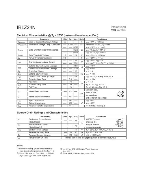
Electrical Characteristics @ T J = 25°C (unless otherwise specified)<br />
Parameter Min Typ Max Units Conditions<br />
V (BR)DSS Drain-to-Source Breakdown Voltage 55 ––– ––– V V GS = 0V, I D = 250µA<br />
∆V (BR)DSS/∆T J Breakdown Voltage Temp Coefficient ––– 0061 ––– V/°C Reference to 25°C, I D = 1mA<br />
––– ––– 0060 V GS = 10V, I D = 11A „<br />
R DS(on) Static Drain-to-Source On-Resistance ––– ––– 0075 Ω V GS = 50V, I D = 11A „<br />
––– ––– 0105 V GS = 40V, I D = 90A „<br />
V GS(th) Gate Threshold Voltage 10 ––– 20 V V DS = V GS , I D = 250µA<br />
g fs Forward Transconductance 83 ––– ––– S V DS = 25V, I D = 11A<br />
I DSS Drain-to-Source Leakage Current<br />
––– ––– 25 V DS = 55V, V GS = 0V<br />
µA<br />
––– ––– 250 V DS = 44V, V GS = 0V, T J = 150°C<br />
I GSS<br />
Gate-to-Source Forward Leakage ––– ––– 100 V GS = 16V<br />
nA<br />
Gate-to-Source Reverse Leakage ––– ––– -100 V GS = -16V<br />
Q g Total Gate Charge ––– ––– 15 I D = 11A<br />
Q gs Gate-to-Source Charge ––– ––– 37 nC V DS = 44V<br />
Q gd Gate-to-Drain ("Miller") Charge ––– ––– 85 V GS = 50V, See Fig 6 and 13 „<br />
t d(on) Turn-On Delay Time ––– 71 ––– V DD = 28V<br />
t r Rise Time ––– 74 ––– I D = 11A<br />
ns<br />
t d(off) Turn-Off Delay Time ––– 20 ––– R G = 12Ω, V GS = 50V<br />
t f Fall Time ––– 29 ––– R D = 24Ω, See Fig 10 „<br />
Between lead,<br />
L D Internal Drain Inductance ––– 45 –––<br />
6mm (025in)<br />
nH<br />
from package<br />
L S Internal Source Inductance ––– 75 –––<br />
and center of die contact<br />
C iss Input Capacitance ––– 480 ––– V GS = 0V<br />
C oss Output Capacitance ––– 130 ––– pF V DS = 25V<br />
C rss Reverse Transfer Capacitance ––– 61 ––– ƒ = 10MHz, See Fig 5<br />
G<br />
D<br />
S<br />
Source-Drain Ratings and Characteristics<br />
Parameter Min Typ Max Units Conditions<br />
I S Continuous Source Current MOSFET symbol<br />
––– ––– 18<br />
(Body Diode)<br />
showing the<br />
A<br />
G<br />
I SM Pulsed Source Current integral reverse<br />
––– ––– 72<br />
(Body Diode)<br />
p-n junction diode<br />
V SD Diode Forward Voltage ––– ––– 13 V T J = 25°C, I S = 11A, V GS = 0V „<br />
t rr Reverse Recovery Time ––– 60 90 ns T J = 25°C, I F = 11A<br />
Q rr Reverse RecoveryCharge ––– 130 200 nC di/dt = 100A/µs „<br />
t on Forward Turn-On Time Intrinsic turn-on time is negligible (turn-on is dominated by L S +L D )<br />
D<br />
S<br />
Notes:<br />
Repetitive rating; pulse width limited by<br />
max junction temperature ( See fig 11 )<br />
‚ V DD = 25V, starting T J = 25°C, L = 790µH<br />
R G = 25Ω, I AS = 11A (See Figure 12)<br />
ƒ I SD ≤ 11A, di/dt ≤ 290A/µs, V DD ≤ V (BR)DSS ,<br />
T J ≤ 175°C<br />
„ Pulse width ≤ 300µs; duty cycle ≤ 2%


