Linear Power Amplifiers - High Frequency Electronics
Linear Power Amplifiers - High Frequency Electronics
Linear Power Amplifiers - High Frequency Electronics

You also want an ePaper? Increase the reach of your titles
YUMPU automatically turns print PDFs into web optimized ePapers that Google loves.
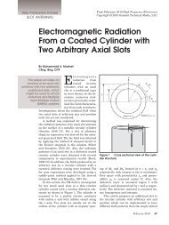
<strong>High</strong> <strong>Frequency</strong> Design<br />
LNA Design<br />
power at the input due to thermal noise from the input<br />
termination. The Noise Figure can be expressed as<br />
Where SNRi and SNRo are the signal to noise ratio at<br />
the input and output of the component and P No<br />
is the total<br />
available power at the output of the amplifier, P Ni<br />
is the<br />
available noise power due to the input termination and<br />
G A<br />
is the Available <strong>Power</strong> Gain.<br />
An alternate method for calculating the Noise Figure<br />
is expressed as<br />
the model. The S parameters and noise parameters were<br />
obtained from the Modelithics nonlinear model at the<br />
desired bias point and frequency. The results are shown<br />
in Table 2 and Table 3 under drain source voltage 3 V and<br />
gate voltage of 0.562 V. For this condition the simulated<br />
drain current from the model is 60 mA.<br />
Table 2 • Model Generated S Parameter Results at 1.9<br />
GHz (Vds = 3V, Vgs = 0.562V, Ids = 60 mA).<br />
F min<br />
, r n<br />
, and Γ opt<br />
are known as noise parameters and<br />
are given by the manufacturer of the transistor or can be<br />
derived experimentally.<br />
To achieve the minimum noise figure, Γ s<br />
= Γ opt<br />
is chosen.<br />
However, simultaneous minimum noise figure and<br />
maximum gain cannot be obtained, in general. Therefore,<br />
the reflection coefficient, Γ s<br />
can be selected that is a compromise<br />
between the Noise Figure and Gain performance<br />
[4]. The Available Gain can be calculated by<br />
Table 3 • Noise Parameters at 1.9 GHz (Vds = 3V, Vgs<br />
= 0.562V, Ids = 60 mA).<br />
The stability factor of the amplifier was simulated<br />
and also calculated by the obtained S-parameters [4]:<br />
For a two port network, unconditional stability is<br />
achieved when these criteria are satisfied: stability factor<br />
K > 1, and |D| > 1. An alternate set of stability criteria<br />
is K > 1 and b >0, with the b corresponding to the<br />
stability measurement given by:<br />
Design Goals<br />
Table 1 shows the design goals for this example LNA.<br />
The design approach and topology followed that determined<br />
by Avago Application Note 1222 as mentioned<br />
above. Series capacitors and parallel inductors were used<br />
for matching networks and a resistive loading method<br />
was chosen to maintain stability. Additionally source<br />
inductance was added to improve the input return loss.<br />
As a result, NF = 0.8 dB and Gain = 16 dB were obtained<br />
by an ADS simulation.<br />
Table 1 • Design Goals.<br />
Device Simulation<br />
Before proceeding to incorporate the application circuit<br />
topology and layout details, device simulation and<br />
stability analysis were performed on the transistor using<br />
Figure 2 graphically shows that the transistor is<br />
potentially unstable at the design frequency band.<br />
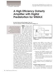
Manufacturer Application Circuit<br />
An application circuit was designed based on the schematic<br />
and component parts list in Table 4 provided by the<br />
manufacturer [3]. Series capacitors and parallel inductors<br />
are used for matching networks. To ensure stability,<br />
resistive loads, 51 ohm and 10 ohm are used to improve<br />
input and output bias networks respectively as shown in<br />
Figure 3 below. The design of these bias networks are<br />
such that the effects of the 51 ohm input bias resistor are<br />
isolated from the RF part of the circuit by a 3.3 nH choke<br />
inductor and a 10 pF bypass capacitor, thus increasing<br />
the noise figure. A combination of 10pF and 10 nF were<br />
used for bypass capacitors.<br />
In addition, source inductance was added for an<br />
improvement of input return loss. The measurement data<br />
of the manufacturer information indicates the potential<br />
for, 16 dB Gain at 1900 MHz, 0.7~0.8 dB Noise Figure<br />
from 1900 MHz through 2000 MHz, -6.4 dB Input Return<br />
Loss and -12.5 dB Output Return Loss under Vds = 3V at<br />
Id = 65mA.<br />
24 <strong>High</strong> <strong>Frequency</strong> <strong>Electronics</strong>