A High-Efficiency Transmission-Line GaN HEMT Class E Power ...
A High-Efficiency Transmission-Line GaN HEMT Class E Power ...
A High-Efficiency Transmission-Line GaN HEMT Class E Power ...

You also want an ePaper? Increase the reach of your titles
YUMPU automatically turns print PDFs into web optimized ePapers that Google loves.
<strong>High</strong> Frequency Design<br />
CLASS E AMPLIFIER<br />
From December 2009 <strong>High</strong> Frequency Electronics<br />
Copyright © 2009 Summit Technical Media, LLC<br />
A <strong>High</strong>-<strong>Efficiency</strong><br />
<strong>Transmission</strong>-<strong>Line</strong> <strong>GaN</strong> <strong>HEMT</strong><br />
<strong>Class</strong> E <strong>Power</strong> Amplifier<br />
By Andrei Grebennikov<br />
Bell Labs Ireland<br />
In modern wireless<br />
This article describes the communication systems<br />
it is required<br />
design of a <strong>Class</strong> E wireless<br />
power amplifier using that the power amplifier<br />
transmission lines for output could operate with high<br />
matching, with the circuit efficiency, high linearity,<br />
implemented using a and low harmonic output<br />
<strong>GaN</strong> <strong>HEMT</strong> transistor level simultaneously. To<br />
increase efficiency of the<br />
power amplifier, a switching-mode <strong>Class</strong> E<br />
mode technique can be applied. This kind of a<br />
power amplifier requires an operation in saturation<br />
mode resulting in a poor linearity, and<br />
therefore is not suitable to directly replace linear<br />
power amplifiers in conventional WCDMA<br />
or CDMA2000 transmitters with non-constant<br />
envelope signal. However, to obtain both high<br />
efficiency and good linearity, a nonlinear highefficiency<br />
power amplifier operating in a <strong>Class</strong><br />
E mode can be used in advanced transmitter<br />
architectures such as Doherty, LINC (linear<br />
amplification using nonlinear components), or<br />
ET (envelope tracking) with digital predistortion<br />
[1-3]. In this paper, a novel transmissionline<br />
load network for a <strong>Class</strong>-E power amplifier<br />
with simple design equations to define its<br />
load-network parameters is presented.<br />
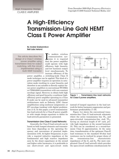
<strong>Transmission</strong>-<strong>Line</strong> <strong>Class</strong>-E Load Networks<br />
Generally, the <strong>Class</strong> E load network can be<br />
based on both lumped elements and transmission<br />
lines depending on the operating frequency<br />
and convenience of practical implementation<br />
[4-6]. At higher frequencies, to provide<br />
a required inductive impedance at the<br />
fundamental and high reactive impedance<br />
seen by the shunt capacitance at the second<br />
and higher order harmonics, it is preferable to<br />
use short-circuit and open-circuit stubs<br />
Figure 1 · <strong>Transmission</strong>-line load networks<br />
for <strong>Class</strong>-E power amplifiers.<br />
instead of lumped capacitors in the load network<br />
for better harmonic suppression and performance<br />
predictability [7-10].<br />
Figure 1(a) shows the conventional transmission-line<br />
<strong>Class</strong> E load-network schematic<br />
where the series transmission line TL 1<br />
and<br />
open-circuited transmission-line stub TL 2<br />
,<br />
having an electrical length of 45° each, provide<br />
high impedance at the second harmonic<br />
[5]. This can be considered as a second-harmonic<br />
<strong>Class</strong> E approximation. At the same<br />
time, transformation of the optimum <strong>Class</strong>-E<br />
load resistance to the standard 50-ohm load<br />
resistance can be realized by proper choice of<br />
the transmission-line characteristic<br />
impedances of the Z 1<br />
and Z 2<br />
. The more complicated<br />
<strong>Class</strong>-E load network which provides<br />
the open-circuit conditions simultaneously for<br />
16 <strong>High</strong> Frequency Electronics
<strong>High</strong> Frequency Design<br />
CLASS E AMPLIFIER<br />
Figure 2 · Modified transmission-line <strong>Class</strong> E power<br />
amplifier.<br />
the second and third harmonics by using a 30-degree<br />
open-circuited stub and a short-circuited quarter wave<br />
transmission line is shown in Figure 1(b) [11].<br />
In the latter case intended for a conventional <strong>Class</strong>-E<br />
mode, the following harmonic conditions seen by the<br />
device output at the fundamental-frequency, second and<br />
third harmonic components must be satisfied:<br />
ImZ<br />
where<br />
net<br />
V<br />
R = 0.<br />
5768<br />
P<br />
( 2ω<br />
)= ImZ<br />
( 3ω<br />
)=∞<br />
0 net 0<br />
2<br />
dd<br />
is the nominal <strong>Class</strong> E load-network resistance, V dd<br />
is the<br />
supply voltage, and P out<br />
is the fundamental-frequency<br />
output power delivered to the load [12]. The device output<br />
capacitance C out<br />
should be equal to the nominal <strong>Class</strong> E<br />
shunt capacitance C defined by<br />
C = 0 . 1836<br />
ω R<br />
<br />
( )<br />
Znet ( ω 0 )= R 1 + jtan 49.<br />
054<br />
0<br />
out<br />
(1)<br />
(2)<br />
(3)<br />
(4)<br />
Figure 3 · Load networks seen by the device output at<br />
harmonic frequencies.<br />
and the transformation to the standard load resistance<br />
R L<br />
= 50 ohms is provided by the proper choice of the loadnetwork<br />
transmission-line characteristic impedances [5,<br />
6]. It should be noted that Eqs. (3) and (4) were obtained<br />
for the idealized optimum (or nominal) zero voltage and<br />
zero voltage-derivative <strong>Class</strong> E conditions when device is<br />
operated as a lossless switch and a series fundamentallytuned<br />
resonant circuit provides an infinite impedance for<br />
the second and higher order harmonics. However, for<br />
example, for the practical transmission-line <strong>Class</strong>-E load<br />
networks shown in Figure 1(a), high impedance can be<br />
provided at the second harmonic only. In this case, the<br />
maximum efficiency can be achieved with nonzero voltage<br />
and voltage-derivative conditions, thus providing a second-harmonic<br />
<strong>Class</strong> E approximation when Eqs. (3) and<br />
(4) can be considered as an initial guess, with the optimum<br />
parameters optimized around these values [4].<br />
Modified Approach: Analysis and Design<br />
The <strong>Class</strong>-E load network shown in Figure 1(b) can be<br />
modified in order to obtain simple analytical equations to<br />
explicitly define the transmission line parameters. Such a<br />
modified transmission-line <strong>Class</strong> E load network is shown<br />
in Figure 2, where the combined series quarterwave<br />
transmission line provides an impedance transformation<br />
at the fundamental frequency, and the open-circuited<br />
stubs with electrical lengths of 90° and 30° create the<br />
18 <strong>High</strong> Frequency Electronics
<strong>High</strong> Frequency Design<br />
CLASS E AMPLIFIER<br />
open-circuit conditions, seen by the device output at the<br />
second and third harmonics, respectively.<br />
Figure 3(a) shows the load network seen by the device<br />
output at the fundamental frequency. Here, the combined<br />
quarter-wavelength series transmission line TL 1<br />
+ TL 2<br />
,<br />
together with an open-circuited capacitive stub TL 4<br />
having<br />
an electrical length of 30°, provides simultaneously a<br />
required inductive reactance and impedance transformation<br />
of the optimum <strong>Class</strong> E load resistance R to the load<br />
resistance R L<br />
by proper choice of the transmission-line<br />
characteristic impedances Z 1<br />
and Z 2<br />
.<br />
The capacitive load impedance Z L<br />
at the end of a quarterwave<br />
line at the fundamental frequency, representing<br />
by the load resistance R L<br />
and capacitive stub TL 4<br />
, can be<br />
written as<br />
Z<br />
L<br />
ZR<br />
2 L<br />
=<br />
Z2 + jR tan 30<br />
where Z 2<br />
is the characteristic impedance of a 30-degree<br />
open-circuit stub. Generally, the input impedance of the<br />
loaded transmission line can be written as<br />
Z = Z Z jZ L<br />
+<br />
1<br />
tan θ<br />
net 1<br />
Z + jZ tan θ<br />
where θ is the electrical length of the transmission line.<br />
Then, substituting Eq. (5) into Eq. (6) for θ = 90° results<br />
in an inductive input impedance<br />
2 2<br />
Z Z<br />
Z = 1<br />
Z<br />
= 1<br />
ZR Z + jR<br />
net 2 L<br />
tan 30<br />
L<br />
1<br />
L<br />
2<br />
L<br />
L<br />
<br />
<br />
( )<br />
when the required optimum <strong>Class</strong>-E resistance can be<br />
provided by proper choice of the characteristic impedance<br />
Z 1<br />
, while the required optimum <strong>Class</strong>-E inductive reactance<br />
can be achieved with the corresponding value of the<br />
characteristic impedance Z 2<br />
.<br />
Separating Eq. (7) into real and imaginary parts<br />
results in the following system of two equations with two<br />
unknown parameters:<br />
(5)<br />
(6)<br />
(7)<br />
Figure 4 · Load network with series inductance at fundamental.<br />
Z<br />
1<br />
=<br />
Z 2<br />
= 05 .<br />
(10)<br />
(11)<br />
where R L<br />
= 50 ohms and R is calculated from Eq. (3).<br />
The transmission-line <strong>Class</strong> E load network seen by<br />
the device output at the second harmonic is shown in<br />
Figure 3(b), taking into account the shorting effect of the<br />
quarterwave short-circuited stub TL 3<br />
, where the transmission<br />
line TL 1<br />
provides an open-circuit condition for<br />
the second harmonic. At the third harmonic, the transmission-line<br />
<strong>Class</strong> E load network can similarly be represented,<br />
as shown in Figure 3(c), due to the open-circuit<br />
effect of the short-circuited quarterwave line TL 3<br />
and<br />
short-circuit effect of the open-circuited harmonic stub<br />
TL 4<br />
at the third harmonic. In this case, the combined<br />
transmission line TL 1<br />
+ TL 2<br />
provides an open-circuit condition<br />
for the third harmonic at the device output being<br />
shorted at its right-hand side.<br />
However, in a common case, it is necessary to take into<br />
account the transistor output parasitic series bondwire<br />
and lead inductance L out<br />
shown in Figure 4, which provides<br />
an additional inductive reactance at the fundamental<br />
and does not affect the open-circuit conditions at the<br />
second and third harmonics. The inductive effect at the<br />
input of the series quarterwave transmission line should<br />
be reduced by proper changing of the characteristic<br />
impedance Z 2<br />
. In this case, Eq. (9) can be rewritten as<br />
Im Z<br />
net<br />
R R L<br />
R L<br />
2<br />
Z1<br />
= + ω0L<br />
3Z<br />
2<br />
out<br />
(12)<br />
Re Z<br />
Z<br />
2<br />
= 1<br />
net<br />
R L<br />
(8)<br />
Hence, by using Eqs. (1) and (10), the characteristic<br />
impedance Z 2<br />
can now be calculated from<br />
Im Z<br />
Z<br />
2<br />
= 1<br />
net<br />
3Z<br />
2<br />
(9)<br />
Z<br />
2<br />
=<br />
R<br />
2<br />
L<br />
1<br />
0L<br />
1 − ω out<br />
1.1586R<br />
(13)<br />
which allows direct calculation of the characteristic<br />
impedances Z 1<br />
and Z 2<br />
. As a result, by using Eq. (1),<br />
resulting in higher characteristic impedance of the opencircuited<br />
stub for greater values of series inductance L out<br />
.<br />
20 <strong>High</strong> Frequency Electronics
Figure 5 · Circuit schematic of <strong>Class</strong> E <strong>GaN</strong> <strong>HEMT</strong> power amplifier.<br />
Simulation<br />
Figure 5 shows the simulated circuit schematic of a<br />
transmission-line <strong>Class</strong> E power amplifier based on a<br />
28 V 5 W Nitronex NPTB00004 <strong>GaN</strong> <strong>HEMT</strong> power transistor.<br />
The input matching circuit with an open-circuited<br />
stub and a series transmission line provides a complexconjugate<br />
matching with the standard 50-ohm source.<br />
The load network represents the modified transmission-
<strong>High</strong> Frequency Design<br />
CLASS E AMPLIFIER<br />
Figure 7 · Test board of <strong>Class</strong> E <strong>GaN</strong> <strong>HEMT</strong> power<br />
amplifier.<br />
Figure 6 · Simulated results for <strong>Class</strong> E <strong>GaN</strong> <strong>HEMT</strong><br />
power amplifier.<br />
line <strong>Class</strong>-E load network shown in Figure 2.<br />
Figure 6 shows the simulated results of a transmission-line<br />
<strong>Class</strong> E power amplifier using a RO4350 30-mil<br />
substrate. The maximum output power of 37 dBm, drain<br />
efficiency of 73% and power-added efficiency (PAE) of 71%<br />
at the center bandwidth frequency of 2.14 GHz are<br />
achieved with a power gain of 14 dB (linear gain of 19 dB)<br />
and a supply voltage of 25 V.<br />
Implementation and Test<br />
The transmission-line <strong>Class</strong> E power amplifier was<br />
fabricated on a RO4350 30-mil substrate. Figure 7 shows<br />
the test board of this power amplifier using a 5 W <strong>GaN</strong><br />
<strong>HEMT</strong> NPTB00004 device. The input matching circuit,<br />
output load network, and gate and drain bias circuits<br />
(with bypass capacitors on their ends) are fully based on<br />
microstrip lines of different electrical lengths and characteristic<br />
impedances, according to the simulation setup<br />
shown in Figure 5.<br />
Figure 8 shows the measured results with a maximum<br />
output power of 37 dBm, a drain efficiency of 70%, and a<br />
PAE of 61.5% with a power gain of 9.5 dB at the operating<br />
frequency of 2.14 GHz (gate bias voltage V g<br />
= –1.4 V,<br />
Figure 8 · Measured results for <strong>Class</strong> E power amplifier<br />
at 2.14 GHz.<br />
Figure 9 · Measured output power and drain efficiency<br />
versus supply voltage.<br />
22 <strong>High</strong> Frequency Electronics
<strong>High</strong> Frequency Design<br />
CLASS E AMPLIFIER<br />
quiescent current I q<br />
= 20 mA, and drain supply voltage<br />
V dd<br />
= 25 V), achieved without any tuning of the input<br />
matching circuit and load network. In this case, the deeper<br />
the saturation mode, the lower DC supply current is<br />
measured, resulting in an increasing drain efficiency<br />
(70% and higher) with almost constant fundamental output<br />
power. The slightly lower power gain is explained by<br />
some mismatch at the input due to effect of the lead<br />
inductance of the packaged transistor.<br />
Figure 9 shows the measured output power and drain<br />
efficiency versus dc supply voltage at the operating frequency<br />
of 2.14 GHz when an input power P in<br />
was set to<br />
27.5 dBm. The fundamental output power is varied<br />
almost linearly from 35 dBm at V dd<br />
= 20 V up to almost<br />
39 dBm at V dd<br />
= 35 V. In this case, the maximum drain<br />
efficiency of 70% is achieved at an optimum DC supply<br />
voltage of 25 V.<br />
Author Information<br />
Andrei Grebennikov received the MSc degree in electronics<br />
from Moscow Institute of Physics and Technology,<br />
and the Ph.D. degree in radio engineering from Moscow<br />
Technical University of Communications and Informatics.<br />
He can be reached by e-mail at: grandrei@ ieee.org<br />
References<br />
1. Y.-S. Lee, M.-W. Lee, and Y.-H. Jeong, “<strong>High</strong>ly efficient<br />
Doherty amplifier based on <strong>Class</strong>-E topology for<br />
WCDMA applications,” IEEE Microwave and Wireless<br />
Components Lett., vol. 18, pp. 608-610, Sept. 2008.<br />
2. C.-T. Chen, C.-J. Li, T.-S. Horng, J.-K. Jau, and J.-Y.<br />
Li, “Design and linearization of <strong>Class</strong>-E power amplifier<br />
for nonconstant envelope modulation,” IEEE Trans.<br />
Microwave Theory Tech., vol. MTT-57, pp. 957-964, Apr.<br />
2009.<br />
3. N. Ui and S. Sano, “A 45% drain efficiency, -50dBc<br />
ACLR <strong>GaN</strong> <strong>HEMT</strong> <strong>Class</strong>-E amplifier with DPD for W-<br />
CDMA base station,” 2006 IEEE MTT-S Int. Microwave<br />
Symp. Dig., vol. 2, pp. 718-721.<br />
4. A. Grebennikov and N. O. Sokal, Switchmode RF<br />
<strong>Power</strong> Amplifiers, New York: Newnes, 2007.<br />
5. T. B. Mader, E. W. Bryerton, M. Markovic, M.<br />
Forman, and Z. Popovic, “Switched-mode high-efficiency<br />
microwave power amplifiers in a free-space power-combiner<br />
array,” IEEE Trans. Microwave Theory Tech., vol.<br />
MTT-46, pp. 1391-1398, Oct. 1998.<br />
6. R. Negra, F. M. Ghannouchi, and W. Bachtold,<br />
“Study and design optimization of multiharmonic transmission-line<br />
load networks for <strong>Class</strong>-E and <strong>Class</strong>-F K-<br />
band MMIC power amplifiers,” IEEE Trans. Microwave<br />
Theory Tech., vol. MTT-55, pp. 1390-1397, June 2007.<br />
7. A. J. Wilkinson and J. K. A. Everard, “<strong>Transmission</strong>line<br />
load-network topology for <strong>Class</strong>-E power amplifiers,”<br />
IEEE Trans. Microwave Theory Tech., vol. MTT-49, pp.<br />
1202-1210, June 2001.<br />
8. J. Lee, S. Kim, J. Nam, J. Kim, I. Kim, and B. Kim,<br />
“<strong>High</strong>ly efficient LDMOS power amplifier based on <strong>Class</strong>-<br />
E topology,” Microwave and Optical Technology Lett., vol.<br />
48, pp. 789-791, Apr. 2006.<br />
9. H. G. Bae, R. Negra, S. Boumaiza, and F. M.<br />
Ghannouchi “<strong>High</strong>-efficiency <strong>GaN</strong> <strong>Class</strong>-E power amplifier<br />
with compact harmonic-suppression network,” Proc.<br />
37th Europ. Microwave Conf., pp. 1093-1096, 2007.<br />
10. Y.-S. Lee and Y.-H. Jeong, “A high-efficiency <strong>Class</strong>-<br />
E <strong>GaN</strong> <strong>HEMT</strong> power amplifier for WCDMA applications,”<br />
IEEE Microwave and Wireless Components Lett., vol. 17,<br />
pp. 622-624, Aug. 2007.<br />
11. P. Aflaki, H. G. Bae, R. Negra, and F. M.<br />
Ghannouchi, “Novel compact transmission-line output<br />
network topology for <strong>Class</strong>-E power amplifiers,” Proc.<br />
38th Europ. Microwave Conf., pp. 238-241, 2008.<br />
12. F. H. Raab, “Idealized operation of the <strong>Class</strong> E<br />
tuned power amplifier,” IEEE Trans. Circuits and<br />
Systems, vol. CAS-24, pp. 725-735, Dec. 1977.<br />
Subscription Information<br />
Subscriptions to <strong>High</strong> Frequency Electronics are free to professionals working in the frequency ranges that typically<br />
involve RF, microwave, high speed analog, high speed digital, and optical electronics. To request a free<br />
subscription, complete the subscription form attached to the cover of this issue, or go online to our web site and<br />
click on the “Subscriptions” tab. You may also e-mail a request to: circulation@highfrequencyelectronics.com<br />
The subscription form must be complete. All subscriptions are subject to publisher’s approval.<br />
www.highfrequencyelectronics.com<br />
24 <strong>High</strong> Frequency Electronics