Linear Power Amplifiers for Point-to-Point Radio ... - RF Micro Devices
Linear Power Amplifiers for Point-to-Point Radio ... - RF Micro Devices
Linear Power Amplifiers for Point-to-Point Radio ... - RF Micro Devices

You also want an ePaper? Increase the reach of your titles
YUMPU automatically turns print PDFs into web optimized ePapers that Google loves.
High Frequency Design<br />
<strong>Power</strong> Amps<br />
<strong>Linear</strong> <strong>Power</strong> <strong>Amplifiers</strong> <strong>for</strong><br />
<strong>Point</strong>-<strong>to</strong>-<strong>Point</strong> <strong>Radio</strong><br />
Applications<br />
By Sushil Kumar, Kent S<strong>to</strong>ry, Ron Kielmeyer, Tariq Lodhi, and Ian Hardcastle—mmW<br />
Solutions Team, <strong>RF</strong>MD<br />
<strong>Micro</strong>wave links in<br />
There is a need <strong>to</strong> the range of 10 – 27 GHz<br />
develop a new are commonly used <strong>for</strong><br />
generation of highly point-<strong>to</strong>-point (P2P) connectivity.<br />
With the phe-<br />
linear, high frequency<br />
chipsets <strong>to</strong> address nomenal increase of cell<br />
traffic congestion. phone users and demand<br />
<strong>for</strong> high data rates, link<br />
traffic is getting congested. Since available<br />
channel bandwidth is limited and fixed, link<br />
manufacturers are addressing this traffic<br />
congestion by increasing spectral efficiency<br />
and are using a complex modulation scheme<br />
such as 4 – 1024 QAM.<br />
In order <strong>to</strong> support this high order modulation<br />
scheme, there is a need <strong>to</strong> develop a<br />
new generation of highly linear, high frequency<br />
chipsets starting from baseband <strong>to</strong><br />
antenna <strong>for</strong> Tx path and from antenna <strong>to</strong><br />
baseband <strong>for</strong> Rx path.<br />
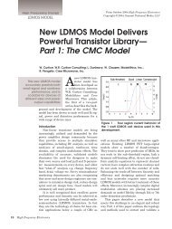
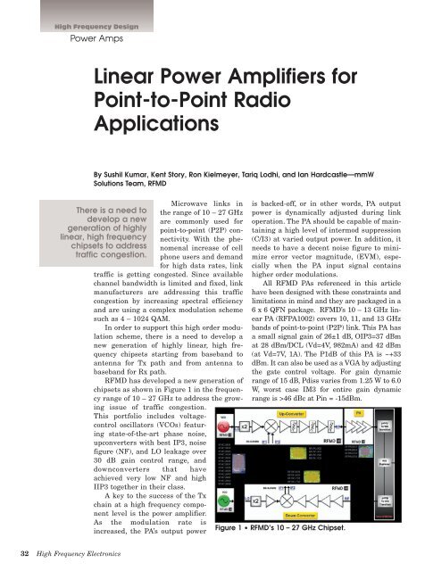
<strong>RF</strong>MD has developed a new generation of<br />
chipsets as shown in Figure 1 in the frequency<br />
range of 10 – 27 GHz <strong>to</strong> address the growing<br />
issue of traffic congestion.<br />
This portfolio includes voltagecontrol<br />
oscilla<strong>to</strong>rs (VCOs) featuring<br />
state-of-the-art phase noise,<br />
upconverters with best IP3, noise<br />
figure (NF), and LO leakage over<br />
30 dB gain control range, and<br />
downconverters that have<br />
achieved very low NF and high<br />
IIP3 <strong>to</strong>gether in their class.<br />
A key <strong>to</strong> the success of the Tx<br />
chain at a high frequency component<br />
level is the power amplifier.<br />
As the modulation rate is<br />
increased, the PA’s output power<br />
is backed-off, or in other words, PA output<br />
power is dynamically adjusted during link<br />
operation. The PA should be capable of maintaining<br />
a high level of intermod suppression<br />
(C/I3) at varied output power. In addition, it<br />
needs <strong>to</strong> have a decent noise figure <strong>to</strong> minimize<br />
error vec<strong>to</strong>r magnitude, (EVM), especially<br />
when the PA input signal contains<br />
higher order modulations.<br />
All <strong>RF</strong>MD PAs referenced in this article<br />
have been designed with these constraints and<br />
limitations in mind and they are packaged in a<br />
6 x 6 QFN package. <strong>RF</strong>MD’s 10 – 13 GHz linear<br />
PA (<strong>RF</strong>PA1002) covers 10, 11, and 13 GHz<br />
bands of point-<strong>to</strong>-point (P2P) link. This PA has<br />
a small signal gain of 26±1 dB, OIP3=37 dBm<br />
at 28 dBm/DCL (Vd=4V, 982mA) and 42 dBm<br />
(at Vd=7V, 1A). The P1dB of this PA is ~+33<br />
dBm. It can also be used as a VGA by adjusting<br />
the gate control voltage. For gain dynamic<br />
range of 15 dB, Pdiss varies from 1.25 W <strong>to</strong> 6.0<br />
W, worst case IM3 <strong>for</strong> entire gain dynamic<br />
range is >46 dBc at Pin = -15dBm.<br />
Figure 1 • <strong>RF</strong>MD’s 10 – 27 GHz Chipset.<br />
32 High Frequency Electronics
High Frequency Design<br />
<strong>Power</strong> Amps<br />
The <strong>RF</strong>PA1003 is a 14.4 - 15.4 GHz high linearity PA<br />
and it has been designed <strong>for</strong> 15 GHz band P2P link. It<br />
has 25 dB gain, IM3=50dBc at P OUT<br />
=20dBm/DCL and<br />
35dBc at P OUT<br />
=28dBm/DCL. P1dB of this PA is +32.5<br />
dBm and OIP3=42.5 dBm at P OUT<br />
=28dBm/DCL.<br />
The <strong>RF</strong>PA1702 is a 17.7 - 19.7 GHz linear PA. It is<br />
designed <strong>for</strong> 18 GHz P2P link. It has 25 dB gain,<br />
IM3=52dBc at P OUT<br />
=20dBm/DCL and 32.5dBc at<br />
P OUT<br />
=27dBm/DCL. P1dB of this PA is +31.0 dBm and<br />
OIP3=41dBm at P OUT<br />
=28dBm/DCL. Its power dissipation<br />
is ~7.0 W and NF~7.0 dB. With over 15 dB gain<br />
control, it consumes 2 <strong>to</strong> 6W dc power and OIP3 varies<br />
from 20 <strong>to</strong> 40 dBm. The minimum IM3 is >55dBc <strong>for</strong><br />
Pin=-15dBm/DCL. All of these PAs have been internally<br />
fabricated using 0.25µm PHEMT technology and packaged<br />
in a 6 x 6 QFN package.<br />
Circuit Design<br />
The key <strong>to</strong> circuit design is the device model. This<br />
model should be able <strong>to</strong> accurately predict small and<br />
large signal behavior including<br />
P1dB and IM3. The model, which is<br />
developed using DC-IV and<br />
[S]-parameter over various bias<br />
voltages, accurately predicts DC,<br />
[S]-parameters, P1dB and Psat per<strong>for</strong>mance.<br />
Such models usually<br />
over predict IM3, and its con<strong>to</strong>urs<br />
are sometimes severely dislocated<br />
on the Smith Chart compared <strong>to</strong><br />
measured con<strong>to</strong>urs. <strong>RF</strong>MD’s PAs<br />
are designed based on a combination<br />
of measured load-pull data and<br />
modified device models <strong>to</strong> properly<br />
incorporate IM3 behavior and<br />
device scaling based on IM3.<br />
A good technique <strong>to</strong> PA design is<br />
<strong>to</strong> partition the spec in<strong>to</strong> number of<br />
stages and then decide the device<br />
size <strong>for</strong> each stage that should provide<br />
required gain, power, and IM3<br />
per stage and inter-stage drive<br />
ratio. To design a linear power<br />
amplifier one should look <strong>for</strong> high<br />
gain and best possible IM3 <strong>for</strong> specified<br />
output power and each device<br />
should be biased <strong>for</strong> a little higher<br />
Idss compared a saturated power<br />
amplifier design. Normally a saturated<br />
power amplifier is biased<br />
close <strong>to</strong> deep class AB condition.<br />
Agilent’s ADS and Momentum have<br />
been used <strong>to</strong> design power amplifiers<br />
discussed here. Voltage and current<br />
probes have been used at all<br />
parallel nodes feeding and combining<br />
signal and power <strong>to</strong> active<br />
device. This helped <strong>to</strong> determine <strong>to</strong><br />
maintain close <strong>to</strong> identical impedances<br />
at all similar nodes and thus<br />
minimize odd-mode problem. Due<br />
<strong>to</strong> inter-coupling among feed network,<br />
impedance mismatch occurs<br />
that cause odd-mode stability<br />
issues. To suppress odd-mode insta-<br />
34 High Frequency Electronics
High Frequency Design<br />
<strong>Power</strong> Amps<br />
band PAs. Figure 3b shows PA<br />
outline package drawing. The<br />
main objective of PA design was<br />
<strong>to</strong> get the best possible IM3 per<strong>for</strong>mance<br />
at P OUT<br />
(<strong>to</strong>tal) =28<br />
dBm. Better BW or Psat can be<br />
achieved if IM3 is not the main<br />
design criterion.<br />
bility, proper value resis<strong>to</strong>rs have been added at gates<br />
and drains. ADS S-probe method has been used <strong>to</strong> check<br />
inter-stage stability. Figure 2 is an example of the<br />
design steps used <strong>for</strong> design of these PAs. Figure 3a<br />
shows die pho<strong>to</strong>graphs of 10, 11, 13, 15, and 18 GHz<br />
Per<strong>for</strong>mance of 9.8 - 13.3 GHz<br />
<strong>Linear</strong> <strong>Power</strong> Amplifier<br />
(<strong>RF</strong>PA1002)<br />
Figures 4a - 4f show measured<br />
per<strong>for</strong>mance of <strong>RF</strong>PA1002.<br />
This PA covers 10, 11, and 13<br />
GHz bands of P2P application.<br />
All the measurements are taken<br />
at Vd=6.5, Id (<strong>to</strong>tal) =1.07A<br />
unless otherwise noted. Figures<br />
4d - 4f show some of the important<br />
per<strong>for</strong>mance plots of this<br />
PA. Figure 4a shows gain versus<br />
frequency behavior over<br />
temperature and Figure 4b<br />
shows OIP3 versus frequency at<br />
drain voltage from 4 <strong>to</strong> 7V, 0.5<br />
step <strong>for</strong> single carrier level<br />
(SCL) P OUT<br />
= 17dBm (or 20 dBm<br />
<strong>to</strong>tal power).<br />
Table 1 shows DC power dissipation<br />
corresponding <strong>to</strong><br />
Figure 4b. Figure 4c shows<br />
OIP3 improvement with the<br />
increase in DC power dissipation<br />
from 6.8 W <strong>to</strong> 8.5 W, it<br />
shows > 1.5 dBm improvement<br />
in OIP3 especially at lower frequency<br />
and <strong>for</strong> P OUT<br />
= 25dBm/<br />
SCL. The main reason <strong>for</strong> this<br />
improvement could be due <strong>to</strong><br />
slightly mismatched IM3 loadline<br />
between simulation and<br />
measured device output load.<br />
Figures 4d - 4f show measured<br />
per<strong>for</strong>mance of the PA as a<br />
VGA. PA gain has been varied<br />
using gate bias. Figure 4d shows<br />
variation of OIP3 versus gain,<br />
<strong>to</strong>tal gain was varied about 15<br />
dB and OIP3 was measured at<br />
constant input power=-15dBm/DCL. Figure 4e shows<br />
how gain varies with Vg. A >15dB gain dynamic range<br />
has been achieved by adjusting gate bias. Figure 4f<br />
shows change in DC power dissipation with variation of<br />
36 High Frequency Electronics
High Frequency Design<br />
<strong>Power</strong> Amps<br />
gain or drain current. Since Vg is varied <strong>to</strong> get VGA<br />
function, drain current varies with Vg.<br />
Per<strong>for</strong>mance of 14.4 - 15.4 GHz <strong>Linear</strong> <strong>Power</strong> Amplifier<br />
(<strong>RF</strong>PA1003)<br />
Figures 5a - 5f show measured per<strong>for</strong>mance of<br />
<strong>RF</strong>PA1003. This is designed <strong>for</strong> 15 GHz band applications.<br />
All the measurements are taken at Vd=7.5, Id<br />
(<strong>to</strong>tal) =1.05A unless otherwise noted. Figure 5a shows<br />
gain versus frequency per<strong>for</strong>mance and <strong>for</strong> entire band<br />
~25dB gain has been achieved. Figure 5b shows IM3<br />
plots with frequency <strong>for</strong> P OUT<br />
= 17/22 and 25dBm SCL.<br />
This PA demonstrates very high IM3 ~50dBc at P OUT<br />
=<br />
17dBm/SCL and >32dBc at P OUT<br />
= 25dBm/SCL, which is<br />
a key parameter <strong>for</strong> a linear PA. Figure 5c shows OIP3<br />
versus frequency at P OUT<br />
=17/22/25dBm/SCL. Figure 5d<br />
is a plot of P1dB and P3dB versus frequency <strong>for</strong> PA<br />
when PA bias was tuned <strong>for</strong> best IM3 or OIP3. If the PA<br />
38 High Frequency Electronics
High Frequency Design<br />
<strong>Power</strong> Amps<br />
needs <strong>to</strong> be used as a saturated amplifier, P1dB and<br />
P3dB per<strong>for</strong>mance can be improved by tuning bias condition<br />
as a saturated amplifier. Figures 5e and 5f show<br />
per<strong>for</strong>mance of the PA as a VGA. PA gain has been varied<br />
using gate bias.<br />
Per<strong>for</strong>mance of 17.7 - 19.7 GHz <strong>Linear</strong> <strong>Power</strong> Amplifier<br />
(<strong>RF</strong>PA1702)<br />
Figures 6a - 6f show measured per<strong>for</strong>mance<br />
<strong>RF</strong>PA1702. This PA covers 18 GHz band of P2P radio<br />
application. All the measurements are taken at Vd=5.5,<br />
Id (<strong>to</strong>tal) =1.3A unless otherwise noted. Figures 6a - 6c<br />
show the PAs gain and OIP3 (at P OUT<br />
=+15 and +24dBm/<br />
SCL) versus frequency behavior over temperature.<br />
Figure 6c shows P1dB and P3dB behavior of the PA<br />
when biased <strong>to</strong> achieve best IM3 per<strong>for</strong>mance. Figures<br />
6e - 6f show per<strong>for</strong>mance of the PA as a VGA. PA gain<br />
has been varied using gate bias.<br />
P OUT<br />
= 22/21 and 20<br />
dBm <strong>for</strong> the various<br />
bands. P1dB and<br />
Psat was measured<br />
under best IM3 tuned<br />
case, if the amp needs<br />
<strong>to</strong> be used as a saturated<br />
amplifier a different<br />
biasing scheme<br />
can be used <strong>for</strong> better<br />
P OUT<br />
per<strong>for</strong>mance at<br />
the cost of IM3/OIP3.<br />
All PA designs incorporate<br />
on-chip package<br />
compensation<br />
networks <strong>for</strong> good I/O<br />
match and are packaged<br />
in a low-cost 6 x<br />
6 ceramic package <strong>for</strong><br />
better thermal per<strong>for</strong>mance.<br />
Due <strong>to</strong><br />
superior IM3/OIP3<br />
per<strong>for</strong>mance of these PAs, they are well suited <strong>for</strong> high<br />
data rate and complex modulation systems.<br />
About the Authors:<br />
The authors work at <strong>RF</strong>MD, where Sushil Kumar is<br />
Direc<strong>to</strong>r, Engineering; Kent S<strong>to</strong>ry is a Staff Design<br />
Engineer; Ron Kielmeyer is a Staff Design Engineer;<br />
Tariq Lodhi is a Senior Design Engineer; and Ian<br />
Hardcastle is a Staff Design Engineer.<br />
References:<br />
1. http://www.rfmd.com/CS/Documents/<br />
<strong>RF</strong>PA1002DS.pdf<br />
2. http://www.rfmd.com/CS/Documents/<br />
<strong>RF</strong>PA1003DS.pdf<br />
3. http://www.rfmd.com/CS/Documents/<br />
<strong>RF</strong>PA1702DS.pdf<br />
Conclusion<br />
The per<strong>for</strong>mance of <strong>RF</strong>MD’s linear power<br />
amplifiers is summarized in Table 2. These PAs<br />
demonstrate high gain and high IM3/OIP3 values<br />
at high P OUT<br />
(<strong>to</strong>tal) = 28 dBm <strong>for</strong> 10, 11, 13,<br />
and 15 GHz band applications. For 18, 23, and<br />
26 GHz bands, the IM3/OIP3 was measured at<br />
P OUT<br />
(<strong>to</strong>tal) = 27 and 26 dBm. These PAs show<br />
very good per<strong>for</strong>mance as VGAs and, by adjusting<br />
gate bias, a gain dynamic range of >15 dB<br />
can be achieved. These PAs maintain decent<br />
IM3/OIP3 per<strong>for</strong>mance, a much desired feature<br />
<strong>to</strong> dynamically adjust power consumption of a<br />
PA. IM5 per<strong>for</strong>mance of the PAs is >60 dBc at<br />
Table 2 • Summary of <strong>RF</strong>MD’s <strong>Linear</strong> <strong>Power</strong> <strong>Amplifiers</strong>.<br />
40 High Frequency Electronics