Linear Power Amplifier Uses Mirror Predistortion - High Frequency ...
Linear Power Amplifier Uses Mirror Predistortion - High Frequency ...
Linear Power Amplifier Uses Mirror Predistortion - High Frequency ...

Create successful ePaper yourself
Turn your PDF publications into a flip-book with our unique Google optimized e-Paper software.
<strong>High</strong> <strong>Frequency</strong> Design<br />
PA PREDISTORTION<br />
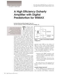
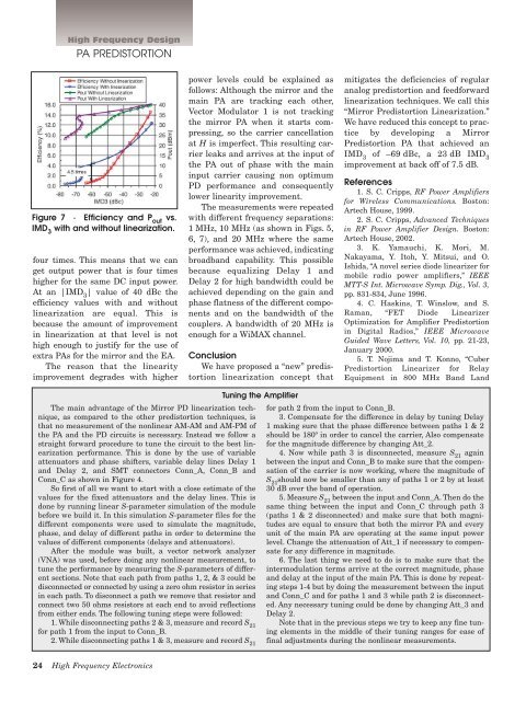
Figure 7 · Efficiency and P out<br />
vs.<br />
IMD 3<br />
with and without linearization.<br />
four times. This means that we can<br />
get output power that is four times<br />
higher for the same DC input power.<br />
At an |IMD 3<br />
| value of 40 dBc the<br />
efficiency values with and without<br />
linearization are equal. This is<br />
because the amount of improvement<br />
in linearization at that level is not<br />
high enough to justify for the use of<br />
extra PAs for the mirror and the EA.<br />
The reason that the linearity<br />
improvement degrades with higher<br />
power levels could be explained as<br />
follows: Although the mirror and the<br />
main PA are tracking each other,<br />
Vector Modulator 1 is not tracking<br />
the mirror PA when it starts compressing,<br />
so the carrier cancellation<br />
at H is imperfect. This resulting carrier<br />
leaks and arrives at the input of<br />
the PA out of phase with the main<br />
input carrier causing non optimum<br />
PD performance and consequently<br />
lower linearity improvement.<br />
The measurements were repeated<br />
with different frequency separations:<br />
1 MHz, 10 MHz (as shown in Figs. 5,<br />
6, 7), and 20 MHz where the same<br />
performance was achieved, indicating<br />
broadband capability. This possible<br />
because equalizing Delay 1 and<br />
Delay 2 for high bandwidth could be<br />
achieved depending on the gain and<br />
phase flatness of the different components<br />
and on the bandwidth of the<br />
couplers. A bandwidth of 20 MHz is<br />
enough for a WiMAX channel.<br />
Conclusion<br />
We have proposed a “new” predistortion<br />
linearization concept that<br />
mitigates the deficiencies of regular<br />
analog predistortion and feedforward<br />
linearization techniques. We call this<br />
“<strong>Mirror</strong> <strong>Predistortion</strong> <strong>Linear</strong>ization.”<br />
We have reduced this concept to practice<br />
by developing a <strong>Mirror</strong><br />
<strong>Predistortion</strong> PA that achieved an<br />
IMD 3<br />
of –69 dBc, a 23 dB IMD 3<br />
improvement at back off of 7.5 dB.<br />
References<br />
1. S. C. Cripps, RF <strong>Power</strong> <strong>Amplifier</strong>s<br />
for Wireless Communications. Boston:<br />
Artech House, 1999.<br />
2. S. C. Cripps, Advanced Techniques<br />
in RF <strong>Power</strong> <strong>Amplifier</strong> Design. Boston:<br />
Artech House, 2002.<br />
3. K. Yamauchi, K. Mori, M.<br />
Nakayama, Y. Itoh, Y. Mitsui, and O.<br />
Ishida, “A novel series diode linearizer for<br />
mobile radio power amplifiers,” IEEE<br />
MTT-S Int. Microwave Symp. Dig., Vol. 3,<br />
pp. 831-834, June 1996.<br />
4. C. Haskins, T. Winslow, and S.<br />
Raman, “FET Diode <strong>Linear</strong>izer<br />
Optimization for <strong>Amplifier</strong> <strong>Predistortion</strong><br />
in Digital Radios,” IEEE Microwave<br />
Guided Wave Letters, Vol. 10, pp. 21-23,<br />
January 2000.<br />
5. T. Nojima and T. Konno, “Cuber<br />
<strong>Predistortion</strong> <strong>Linear</strong>izer for Relay<br />
Equipment in 800 MHz Band Land<br />
Tuning the <strong>Amplifier</strong><br />
The main advantage of the <strong>Mirror</strong> PD linearization technique,<br />
as compared to the other predistortion techniques, is<br />
for path 2 from the input to Conn_B.<br />
that no measurement of the nonlinear AM-AM and AM-PM of<br />
the PA and the PD circuits is necessary. Instead we follow a<br />
straight forward procedure to tune the circuit to the best linearization<br />
performance. This is done by the use of variable<br />
attenuators and phase shifters, variable delay lines Delay 1<br />
and Delay 2, and SMT connectors Conn_A, Conn_B and<br />
Conn_C as shown in Figure 4.<br />
So first of all we want to start with a close estimate of the<br />
values for the fixed attenuators and the delay lines. This is<br />
done by running linear S-parameter simulation of the module<br />
before we build it. In this simulation S-parameter files for the<br />
different components were used to simulate the magnitude,<br />
phase, and delay of different paths in order to determine the<br />
values of different components (delays and attenuators).<br />
After the module was built, a vector network analyzer<br />
(VNA) was used, before doing any nonlinear measurement, to<br />
tune the performance by measuring the S-parameters of different<br />
sections. Note that each path from paths 1, 2, & 3 could be<br />
disconnected or connected by using a zero ohm resistor in series<br />
in each path. To disconnect a path we remove that resistor and<br />
connect two 50 ohms resistors at each end to avoid reflections<br />
from either ends. The following tuning steps were followed:<br />
1. While disconnecting paths 2 & 3, measure and record S 21<br />
for path 1 from the input to Conn_B.<br />
2. While disconnecting paths 1 & 3, measure and record S 21<br />
3. Compensate for the difference in delay by tuning Delay<br />
1 making sure that the phase difference between paths 1 & 2<br />
should be 180º in order to cancel the carrier, Also compensate<br />
for the magnitude difference by changing Att_2.<br />
4. Now while path 3 is disconnected, measure S 21<br />
again<br />
between the input and Conn_B to make sure that the compensation<br />
of the carrier is now working, where the magnitude of<br />
S 21<br />
should now be smaller than any of paths 1 or 2 by at least<br />
30 dB over the band of operation.<br />
5. Measure S 21<br />
between the input and Conn_A. Then do the<br />
same thing between the input and Conn_C through path 3<br />
(paths 1 & 2 disconnected) and make sure that both magnitudes<br />
are equal to ensure that both the mirror PA and every<br />
unit of the main PA are operating at the same input power<br />
level. Change the attenuation of Att_1 if necessary to compensate<br />
for any difference in magnitude.<br />
6. The last thing we need to do is to make sure that the<br />
intermodulation terms arrive at the correct magnitude, phase<br />
and delay at the input of the main PA. This is done by repeating<br />
steps 1-4 but by doing the measurement between the input<br />
and Conn_C and for paths 1 and 3 while path 2 is disconnected.<br />
Any necessary tuning could be done by changing Att_3 and<br />
Delay 2.<br />
Note that in the previous steps we try to keep any fine tuning<br />
elements in the middle of their tuning ranges for ease of<br />
final adjustments during the nonlinear measurements.<br />
24 <strong>High</strong> <strong>Frequency</strong> Electronics