Linear Power Amplifier Uses Mirror Predistortion - High Frequency ...
Linear Power Amplifier Uses Mirror Predistortion - High Frequency ...
Linear Power Amplifier Uses Mirror Predistortion - High Frequency ...

Create successful ePaper yourself
Turn your PDF publications into a flip-book with our unique Google optimized e-Paper software.
<strong>High</strong> <strong>Frequency</strong> Design<br />
PA PREDISTORTION<br />
From June 2011 <strong>High</strong> <strong>Frequency</strong> Electronics<br />
Copyright © 2011 Summit Technical Media, LLC<br />
<strong>Linear</strong> <strong>Power</strong> <strong>Amplifier</strong><br />
<strong>Uses</strong> <strong>Mirror</strong> <strong>Predistortion</strong><br />
By Khaled Fayed, Amin Ezzeddine, and Ho Huang, AMCOM Communications Inc.,<br />
and Amir Zaghloul, U.S. Army Research Laboratory and Virginia Tech<br />
Current wireless<br />
This article describes a communication<br />
hybrid power amplifier standards have<br />
linearization method that been established to carry<br />
combines analog predistortion<br />
and feedforward high data rates. These<br />
voice, data and video with<br />
design concepts high data rates require<br />
efficient modulation techniques<br />
such as OFDM 64 QAM, to allow transmission<br />
in a given finite bandwidth. With<br />
these types of modulation, there are probabilities<br />
that at certain times, the voltages of the<br />
multiple carriers are in phase and their amplitudes<br />
add up to create a very high peak to<br />
average ratio (PAR) that may reach 15 dB.<br />
This high PAR will drive a conventional PA<br />
into saturation; causing signal distortion and<br />
generating out-band interference. One way to<br />
solve this problem is to use a high power PA in<br />
Class A mode, with average power set at a<br />
back off (BO) of 10-12 dB. Unfortunately, this<br />
technique results in a very inefficient PA.<br />
There are various linearization techniques<br />
that are used to increase the linearity of the<br />
PA allowing the use at lower BO values and<br />
consequently having higher efficiency. These<br />
techniques include feedback, feedforward, digital<br />
predistortion or analog predistortion [1, 2].<br />
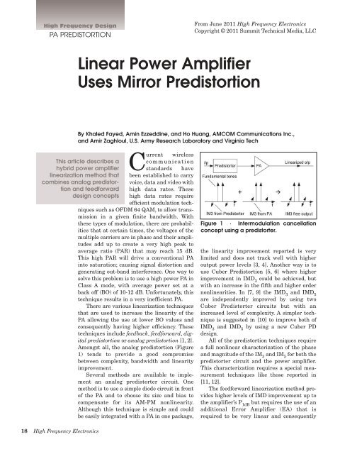
Amongst all, the analog predistortion (Figure<br />
1) tends to provide a good compromise<br />
between complexity, bandwidth and linearity<br />
improvement.<br />
Several methods are available to implement<br />
an analog predistorter circuit. One<br />
method is to use a simple diode circuit in front<br />
of the PA and to choose its size and bias to<br />
compensate for its AM-PM nonlinearity.<br />
Although this technique is simple and could<br />
be easily integrated with a PA in one package,<br />
Figure 1 · Intermodulation cancellation<br />
concept using a predistorter.<br />
the linearity improvement reported is very<br />
limited and does not track well with higher<br />
output power levels [3, 4]. Another way is to<br />
use Cuber <strong>Predistortion</strong> [5, 6] where higher<br />
improvement in IMD 3<br />
could be achieved, but<br />
with an increase in the fifth and higher order<br />
nonlinearities. In [7, 9] the IMD 3<br />
and IMD 5<br />
are independently improved by using two<br />
Cuber Predistorter circuits but with an<br />
increased level of complexity. A simpler technique<br />
is suggested in [10] to improve both of<br />
IMD 3<br />
and IMD 5<br />
by using a new Cuber PD<br />
design.<br />
All of the predistortion techniques require<br />
a full nonlinear characterization of the phase<br />
and magnitude of the IM 3<br />
and IM 5<br />
for both the<br />
predistorter circuit and the power amplifier.<br />
This characterization requires a special measurement<br />
techniques like those reported in<br />
[11, 12].<br />
The feedforward linearization method provides<br />
higher levels of IMD improvement up to<br />
the amplifier’s P 1dB<br />
but requires the use of an<br />
additional Error <strong>Amplifier</strong> (EA) that is<br />
required to be very linear and consequently<br />
18 <strong>High</strong> <strong>Frequency</strong> Electronics
<strong>High</strong> <strong>Frequency</strong> Design<br />
PA PREDISTORTION<br />
Figure 2 · <strong>Mirror</strong> predistortion linearization block diagram.<br />
consumes a lot of power, resulting in<br />
reduction in the overall efficiency of<br />
the PA. This article describes a pseudo-predistortion<br />
linearization technique<br />
that mitigates the deficiencies<br />
of both analog predistortion and feedforward<br />
techniques.<br />
We suggest using a low power PA<br />
in front of the main high power PA.<br />
This low power PA has identical construction<br />
as the main PA and, therefore,<br />
has the same distortion characteristics,<br />
but at a lower power level.<br />
Because this low power PA’s third<br />
and higher order nonlinearities mirror<br />
those of the main PA in magnitude<br />
and phase, we call this low<br />
power PA a “<strong>Mirror</strong> Predistorter.” The<br />
nonlinearities generated by the mirror<br />
PD are properly fed to the input of<br />
the PA, so that they appear at its<br />
output in the same magnitude but<br />
out of phase with the internally generated<br />
PA nonlinearities, resulting in<br />
IM cancellation as shown in Figure 1.<br />
Circuit Implementation<br />
In order to prove the concept of<br />
the proposed mirror PD, we have<br />
designed a mirror predistortion PA.<br />
Figure 2 shows the block diagram of<br />
the proposed mirror PD linearization<br />
technique. The intermodulation<br />
terms coming from the mirror PD<br />
must be fed to the input signal of the<br />
PA so that they cancel the intermodulation<br />
products generated at the<br />
output. So the magnitudes of paths<br />
ABDFHIK and ACJK must be equal,<br />
but with the phases shifted by 180°.<br />
Both the magnitude and the phase<br />
are controlled by Vector Modulator 2,<br />
whereas Delay 2 is used to equalize<br />
the time delay of the two paths.<br />
Also, it is necessary to cancel the<br />
carrier coming out from the mirror<br />
PA. This is done by adding path EG to<br />
path DF with the same delay and<br />
magnitude, but with a 180° phase<br />
shift. Again, this is controlled by<br />
using Vector Modulator 1 and Delay 1<br />
to get broadband cancellation. Any<br />
carrier leakage at point H will result<br />
in reduced gain since paths<br />
ABDFHIK and ACJK are 180° out of<br />
phase, and also will result in nonoptimum<br />
predistorter tracking to the<br />
AM-AM and AM-PM of the PA.<br />
The main advantage of the <strong>Mirror</strong><br />
PD over feedforward linearization is<br />
that the size of the Error <strong>Amplifier</strong><br />
(EA) could be much smaller in terms<br />
of size and power consumption<br />
because the EA is in the input (low<br />
power) side. This is accomplished by<br />
feeding the intermodulation terms at<br />
Figure 3 · Realizing a <strong>Mirror</strong> PA that<br />
has the same nonlinear characteristics<br />
as the main PA.<br />
the input of the PA rather than its<br />
output. So the power requirement of<br />
the EA is lower by an amount that is<br />
equal to the gain of the main PA.<br />
Moreover by changing the coupling<br />
ratio of coupler IKJ we can further<br />
decrease the requirement on the output<br />
power of the EA. However by<br />
doing so, the total loss of the PD will<br />
increase. For instance if we are using<br />
a 10 dB coupler instead of a 3 dB coupler,<br />
the total loss of the predistorter<br />
will be 7 dB greater.<br />
If necessary, the total gain of the<br />
PA with the predistorter could be<br />
boosted by using a low power driver<br />
amplifier before the predistorter.<br />
The mirror PA is an AMCOM<br />
MMIC PA, AM204437WM-BM. It has<br />
30 dB gain with 36 dBm output<br />
power from 2.0 to 4.4 GHz. The main<br />
PA combines of four of the same<br />
MMICs as shown in Figure 3.<br />
Therefore, the DC power consump-<br />
AMCOM AM204437WM-BM (used for Main and <strong>Mirror</strong> PA)<br />
Features: Wide bandwidth from 2.0 to 4.4 GHz<br />
<strong>High</strong> output power, P sat<br />
= 37 dBm<br />
<strong>High</strong> gain, 30 dB<br />
Fully matched; 50-ohm input/output impedance<br />
Ceramic package, RoHS compliant<br />
AMCOM AM304031WM-BM (used for EA)<br />
Features: Wide bandwidth from 2.6 to 4.6 GHz<br />
<strong>High</strong> output power, P 1dB<br />
= 32 dBm<br />
<strong>High</strong> gain, 31 dB<br />
Fully matched; 50-ohm input/output impedance<br />
Ceramic package, RoHS compliant<br />
Table 1 · Specifications of the Main, <strong>Mirror</strong> and Error amplifier MMICs.<br />
20 <strong>High</strong> <strong>Frequency</strong> Electronics
<strong>High</strong> <strong>Frequency</strong> Design<br />
PA PREDISTORTION<br />
AMCOM MMIC AM304031WM-BM<br />
was used as the EA and consumes<br />
only 22% of the mirror PA DC power,<br />
which is just 5.5% of the main PA<br />
power. Surface mount 3 dB hybrid<br />
couplers with a frequency band of 3.3<br />
to 3.7 GHz were used everywhere in<br />
the design except for coupler IKJ<br />
where a 10 dB coupler was used to<br />
lower the output power from the EA<br />
at the expense of higher PD loss. The<br />
vector modulators consist of analog<br />
voltage attenuators and analog phase<br />
shifters. Both of them were designed<br />
using 3 dB hybrid coupler and two<br />
PIN diodes for the variable attenuator,<br />
plus two varactors for the variable<br />
phase shifter by using the reflective<br />
topology as described in [7].<br />
Figure 4 · Layout diagram and photo of the implemented hybrid module.<br />
tion of the mirror PA is only 1/4 of the<br />
main PA. The overall efficiency can<br />
be improved if the main PA is implemented<br />
by combining eight MMICs.<br />
The input power of the MMIC used in<br />
the mirror PA must be equal to the<br />
input power of each of the same<br />
MMICs used in the main PA (P A0<br />
=<br />
P A1-4<br />
), otherwise the nonlinear performance<br />
will be different. This could<br />
Figure 5 · IMD 3<br />
vs. output power<br />
with and without linearization.<br />
be adjusted by an additional fixed<br />
attenuator in front of the mirror PA<br />
according to the coupling factors of<br />
the different couplers used in the<br />
design. Table 1 shows the key specifications<br />
of the MMIC amplifier modules<br />
used in the PA.<br />
The mirror predistortion PA was<br />
integrated in a hybrid module that is<br />
6.1” × 2.9” (Figure 4). A low power<br />
Figure 6 · IMD 5<br />
vs. output power<br />
with and without linearization.<br />
Experimental Results<br />
Figures 5 and 6 show the IMD 3<br />
and IMD 5<br />
versus two-tone total output<br />
power for this mirror predistortion<br />
PA, with and without linearization.<br />
The linearization is being activated<br />
and deactivated by turning on<br />
and off the EA. The frequency separation<br />
of the two tones is 10 MHz. We<br />
are able to optimize the performance<br />
at different back off levels by controlling<br />
the vector modulators. For the<br />
results shown, the performance is<br />
optimized at 34 dBm, which is 7.5 dB<br />
back off from the output 1 dB compression<br />
power of 41.5 dBm. At a twotone<br />
total output power of 34 dBm,<br />
the IMD 3<br />
is –46 dBc where the IMD 5<br />
is –72 dBc when the linearization is<br />
deactivated. The IMD 3<br />
is –69 dBc and<br />
the IMD 5<br />
is –75 dBc when the linearization<br />
is activated. This represents<br />
IMD 3<br />
and IMD 5<br />
improvements<br />
of 23 dB and 3 dB, respectively.<br />
Since the main purpose of linearization<br />
is to operate the PA at<br />
lower BO values with the same linearity,<br />
we plot the efficiency and output<br />
power of the PA versus the IMD 3<br />
level with and without linearization<br />
as shown in Figure 7. We notice that<br />
for higher levels of linearity requirements,<br />
i.e. |IMD 3<br />
| > 60 dBc, the<br />
increase in efficiency is more than<br />
22 <strong>High</strong> <strong>Frequency</strong> Electronics
<strong>High</strong> <strong>Frequency</strong> Design<br />
PA PREDISTORTION<br />
Figure 7 · Efficiency and P out<br />
vs.<br />
IMD 3<br />
with and without linearization.<br />
four times. This means that we can<br />
get output power that is four times<br />
higher for the same DC input power.<br />
At an |IMD 3<br />
| value of 40 dBc the<br />
efficiency values with and without<br />
linearization are equal. This is<br />
because the amount of improvement<br />
in linearization at that level is not<br />
high enough to justify for the use of<br />
extra PAs for the mirror and the EA.<br />
The reason that the linearity<br />
improvement degrades with higher<br />
power levels could be explained as<br />
follows: Although the mirror and the<br />
main PA are tracking each other,<br />
Vector Modulator 1 is not tracking<br />
the mirror PA when it starts compressing,<br />
so the carrier cancellation<br />
at H is imperfect. This resulting carrier<br />
leaks and arrives at the input of<br />
the PA out of phase with the main<br />
input carrier causing non optimum<br />
PD performance and consequently<br />
lower linearity improvement.<br />
The measurements were repeated<br />
with different frequency separations:<br />
1 MHz, 10 MHz (as shown in Figs. 5,<br />
6, 7), and 20 MHz where the same<br />
performance was achieved, indicating<br />
broadband capability. This possible<br />
because equalizing Delay 1 and<br />
Delay 2 for high bandwidth could be<br />
achieved depending on the gain and<br />
phase flatness of the different components<br />
and on the bandwidth of the<br />
couplers. A bandwidth of 20 MHz is<br />
enough for a WiMAX channel.<br />
Conclusion<br />
We have proposed a “new” predistortion<br />
linearization concept that<br />
mitigates the deficiencies of regular<br />
analog predistortion and feedforward<br />
linearization techniques. We call this<br />
“<strong>Mirror</strong> <strong>Predistortion</strong> <strong>Linear</strong>ization.”<br />
We have reduced this concept to practice<br />
by developing a <strong>Mirror</strong><br />
<strong>Predistortion</strong> PA that achieved an<br />
IMD 3<br />
of –69 dBc, a 23 dB IMD 3<br />
improvement at back off of 7.5 dB.<br />
References<br />
1. S. C. Cripps, RF <strong>Power</strong> <strong>Amplifier</strong>s<br />
for Wireless Communications. Boston:<br />
Artech House, 1999.<br />
2. S. C. Cripps, Advanced Techniques<br />
in RF <strong>Power</strong> <strong>Amplifier</strong> Design. Boston:<br />
Artech House, 2002.<br />
3. K. Yamauchi, K. Mori, M.<br />
Nakayama, Y. Itoh, Y. Mitsui, and O.<br />
Ishida, “A novel series diode linearizer for<br />
mobile radio power amplifiers,” IEEE<br />
MTT-S Int. Microwave Symp. Dig., Vol. 3,<br />
pp. 831-834, June 1996.<br />
4. C. Haskins, T. Winslow, and S.<br />
Raman, “FET Diode <strong>Linear</strong>izer<br />
Optimization for <strong>Amplifier</strong> <strong>Predistortion</strong><br />
in Digital Radios,” IEEE Microwave<br />
Guided Wave Letters, Vol. 10, pp. 21-23,<br />
January 2000.<br />
5. T. Nojima and T. Konno, “Cuber<br />
<strong>Predistortion</strong> <strong>Linear</strong>izer for Relay<br />
Equipment in 800 MHz Band Land<br />
Tuning the <strong>Amplifier</strong><br />
The main advantage of the <strong>Mirror</strong> PD linearization technique,<br />
as compared to the other predistortion techniques, is<br />
for path 2 from the input to Conn_B.<br />
that no measurement of the nonlinear AM-AM and AM-PM of<br />
the PA and the PD circuits is necessary. Instead we follow a<br />
straight forward procedure to tune the circuit to the best linearization<br />
performance. This is done by the use of variable<br />
attenuators and phase shifters, variable delay lines Delay 1<br />
and Delay 2, and SMT connectors Conn_A, Conn_B and<br />
Conn_C as shown in Figure 4.<br />
So first of all we want to start with a close estimate of the<br />
values for the fixed attenuators and the delay lines. This is<br />
done by running linear S-parameter simulation of the module<br />
before we build it. In this simulation S-parameter files for the<br />
different components were used to simulate the magnitude,<br />
phase, and delay of different paths in order to determine the<br />
values of different components (delays and attenuators).<br />
After the module was built, a vector network analyzer<br />
(VNA) was used, before doing any nonlinear measurement, to<br />
tune the performance by measuring the S-parameters of different<br />
sections. Note that each path from paths 1, 2, & 3 could be<br />
disconnected or connected by using a zero ohm resistor in series<br />
in each path. To disconnect a path we remove that resistor and<br />
connect two 50 ohms resistors at each end to avoid reflections<br />
from either ends. The following tuning steps were followed:<br />
1. While disconnecting paths 2 & 3, measure and record S 21<br />
for path 1 from the input to Conn_B.<br />
2. While disconnecting paths 1 & 3, measure and record S 21<br />
3. Compensate for the difference in delay by tuning Delay<br />
1 making sure that the phase difference between paths 1 & 2<br />
should be 180º in order to cancel the carrier, Also compensate<br />
for the magnitude difference by changing Att_2.<br />
4. Now while path 3 is disconnected, measure S 21<br />
again<br />
between the input and Conn_B to make sure that the compensation<br />
of the carrier is now working, where the magnitude of<br />
S 21<br />
should now be smaller than any of paths 1 or 2 by at least<br />
30 dB over the band of operation.<br />
5. Measure S 21<br />
between the input and Conn_A. Then do the<br />
same thing between the input and Conn_C through path 3<br />
(paths 1 & 2 disconnected) and make sure that both magnitudes<br />
are equal to ensure that both the mirror PA and every<br />
unit of the main PA are operating at the same input power<br />
level. Change the attenuation of Att_1 if necessary to compensate<br />
for any difference in magnitude.<br />
6. The last thing we need to do is to make sure that the<br />
intermodulation terms arrive at the correct magnitude, phase<br />
and delay at the input of the main PA. This is done by repeating<br />
steps 1-4 but by doing the measurement between the input<br />
and Conn_C and for paths 1 and 3 while path 2 is disconnected.<br />
Any necessary tuning could be done by changing Att_3 and<br />
Delay 2.<br />
Note that in the previous steps we try to keep any fine tuning<br />
elements in the middle of their tuning ranges for ease of<br />
final adjustments during the nonlinear measurements.<br />
24 <strong>High</strong> <strong>Frequency</strong> Electronics
Mobile Telephone System,” IEEE<br />
Transactions on Vehicular Technology, VT-<br />
34, no. 4, pp. 169-177, November 1985.<br />
6. K. Morris and P. Kenington, “<strong>Power</strong><br />
amplifier linearisation using predistortion<br />
techniques,” IEEE Colloquium on RF<br />
and Microwave Components for Communication<br />
Systems, Bradford UK, 1997.<br />
7. J. Yi, Y. Yang, M. Park, W. Kang, and<br />
B. Kim, “Analog predistortion linearizer<br />
for high-power RF amplifiers,” IEEE<br />
Trans. Microwave Theory & Tech., Vol. 48,<br />
no. 12, pp. 2709-2713, 2000.<br />
8. S. Y. Lee, Y. S. Lee, S. H. Hong, H. S.<br />
Choi, and Y. H. Jeong “Independently controllable<br />
3rd- and 5th-order analog predistortion<br />
linearizer for RF power amplifier<br />
in GSM,” Proceedings of 2004 IEEE Asia-<br />
Pacific Conference on Advanced System<br />
Integrated Circuits, pp. 146-149, 2004 .<br />
9. Y. S. Lee, K. I. Jeon, and Y. H. Jeong.<br />
“<strong>Linear</strong>ity Improvement of RF <strong>Power</strong><br />
<strong>Amplifier</strong>s Using a Simple <strong>High</strong>-Order<br />
Predistorter for WCDMA Applications,”<br />
Proceeding of 2006 Asia-Pacific Microwave<br />
Conference, vol. 2, pp. 887-890, 2006<br />
10. Y. S. Lee, S. Y. Lee, K. I. Jeon, and<br />
Y. H. Jeong. “<strong>High</strong>ly linear predistortion<br />
power amplifiers with phase-controlled<br />
error generator,” IEEE Microwave &<br />
Wireless Components Letters, vol. 16, no.<br />
12, pp. 690-692, December 2006.<br />
11. S. Y. Lee, Y. S. Lee, and Y. H. Jeong,<br />
“A novel phase measurement Technique<br />
for IM3 Components in RF <strong>Power</strong><br />
<strong>Amplifier</strong>s,” IEEE Trans. Microwave<br />
Theory & Tech, vol. 54, no. 1, pp. 451–457,<br />
January 2006.<br />
12. J. Dunsmore, and D. Goldberg,<br />
“Novel Two-Tone Intermodulation Phase<br />
Measurement for Evaluating <strong>Amplifier</strong><br />
Memory Effects,” 33rd European<br />
Microwave Conference, pp. 235-238,<br />
October 2003.<br />
13. K. Fayed, A. Zaghloul, A. Ezzedine<br />
and H. Huang, “A <strong>Mirror</strong> <strong>Predistortion</strong><br />
<strong>Linear</strong> <strong>Power</strong> <strong>Amplifier</strong>,” WAMICON<br />
2011 Conference Proceedings, April 2011.<br />
Amin Ezzeddine is the Executive<br />
Vice President, Chief Engineer and cofounder<br />
of AMCOM Communications,<br />
Inc. He received his Bachelor of<br />
Science from Ain-Shams University,<br />
Cairo, his Masters Degree in EE and<br />
Doctor of Science degree from MIT. He<br />
has over 28 years experience designing<br />
MMIC and MIC components.<br />
Ho-Chung Huang is President of<br />
AMCOM Communications Inc. He<br />
received his MS and Ph.D. EE from<br />
Cornell University. Dr. Huang has 12<br />
patents and over 100 technical publications<br />
in the microwave area.<br />
Amir I. Zaghloul received his<br />
M.A.Sc. and Ph.D. from University of<br />
Waterloo, Canada, and the B.Sc. from<br />
Cairo University, Egypt. He is currently<br />
with the US Army Research<br />
Laboratory on an IPA agreement<br />
with Virginia Tech.<br />
Author Information<br />
Khaled Fayed received his<br />
Masters Degree in EE from Virginia<br />
Tech in 2009 and currently is a senior<br />
design engineer at AMCOM<br />
Communications Inc. in Maryland,<br />
where he develops MMIC and hybrid<br />
module power amplifiers for broadband,<br />
high power, and high linearity<br />
applications. He can be reached at<br />
khaled@amcomusa.com