The Basics of Probe Measurements on Wafers and Other Substrates
The Basics of Probe Measurements on Wafers and Other Substrates
The Basics of Probe Measurements on Wafers and Other Substrates

Create successful ePaper yourself
Turn your PDF publications into a flip-book with our unique Google optimized e-Paper software.
High Frequency Design<br />
PROBE MEASUREMENTS<br />
From May 2011 High Frequency Electr<strong>on</strong>ics<br />
Copyright © 2011 Summit Technical Media, LLC<br />
<str<strong>on</strong>g>The</str<strong>on</strong>g> <str<strong>on</strong>g>Basics</str<strong>on</strong>g> <str<strong>on</strong>g>of</str<strong>on</strong>g> <str<strong>on</strong>g>Probe</str<strong>on</strong>g><br />
<str<strong>on</strong>g>Measurements</str<strong>on</strong>g> <strong>on</strong> <strong>Wafers</strong><br />
<strong>and</strong> <strong>Other</strong> <strong>Substrates</strong><br />
By Gary Breed<br />
Editorial Director<br />
Microwave measurements<br />
<str<strong>on</strong>g>of</str<strong>on</strong>g>ten<br />
Here is an introducti<strong>on</strong> to<br />
the applicati<strong>on</strong>s <strong>and</strong> technical<br />
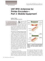
issues for microwave probe (Fig. 1) be used to<br />
require that a<br />
probe measurements <str<strong>on</strong>g>of</str<strong>on</strong>g> c<strong>on</strong>tact the circuit c<strong>on</strong>ductors<br />
<strong>on</strong> the substrate<br />
various circuit types<br />
up<strong>on</strong> which the circuit is<br />
c<strong>on</strong>structed: typically a semic<strong>on</strong>ductor wafer,<br />
ceramic substrate or microwave laminate<br />
material. This tutorial reviews some <str<strong>on</strong>g>of</str<strong>on</strong>g> the<br />
applicati<strong>on</strong>s for these measurements, <strong>and</strong> presents<br />
the key issues affecting measurement<br />
accuracy <strong>and</strong> repeatability.<br />
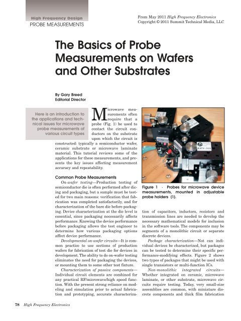
Figure 1 · <str<strong>on</strong>g>Probe</str<strong>on</strong>g>s for microwave device<br />
measurements, mounted in adjustable<br />
probe holders [1].<br />
Comm<strong>on</strong> <str<strong>on</strong>g>Probe</str<strong>on</strong>g> <str<strong>on</strong>g>Measurements</str<strong>on</strong>g><br />
On-wafer testing—Producti<strong>on</strong> testing <str<strong>on</strong>g>of</str<strong>on</strong>g><br />
semic<strong>on</strong>ductor die is <str<strong>on</strong>g>of</str<strong>on</strong>g>ten performed after dicing<br />
<strong>and</strong> packaging, but a sample must be tested<br />
for two main reas<strong>on</strong>s: verificati<strong>on</strong> that fabricati<strong>on</strong><br />
was completed satisfactorily, <strong>and</strong> for<br />
characterizati<strong>on</strong> <str<strong>on</strong>g>of</str<strong>on</strong>g> the bare die before packaging.<br />
Device characterizati<strong>on</strong> at the die level is<br />
essential, since packaging necessarily affects<br />
performance. Knowing the device performance<br />
before packaging allows the test engineer to<br />
determine how various packaging opti<strong>on</strong>s<br />
affect device performance.<br />
Developmental <strong>on</strong>-wafer circuits—It is comm<strong>on</strong><br />
practice to use secti<strong>on</strong>s <str<strong>on</strong>g>of</str<strong>on</strong>g> producti<strong>on</strong><br />
wafers for fabricati<strong>on</strong> <str<strong>on</strong>g>of</str<strong>on</strong>g> test die for devices in<br />
development. <str<strong>on</strong>g>The</str<strong>on</strong>g> ability to do <strong>on</strong>-wafer testing<br />
eliminates the need for packaging the devices,<br />
or mounting them to some other test fixture.<br />
Characterizati<strong>on</strong> <str<strong>on</strong>g>of</str<strong>on</strong>g> passive comp<strong>on</strong>ents—<br />
Individual circuit elements are combined for<br />
any practical RF/microwave/high speed functi<strong>on</strong>.<br />
With the present str<strong>on</strong>g reliance <strong>on</strong> modeling<br />
<strong>and</strong> simulati<strong>on</strong> prior to actual fabricati<strong>on</strong><br />
<strong>and</strong> prototyping, accurate characterizati<strong>on</strong><br />
<str<strong>on</strong>g>of</str<strong>on</strong>g> capacitors, inductors, resistors <strong>and</strong><br />
transmissi<strong>on</strong> lines are needed to develop the<br />
necessary mathematical models for inclusi<strong>on</strong><br />
in the s<str<strong>on</strong>g>of</str<strong>on</strong>g>tware tools. <str<strong>on</strong>g>The</str<strong>on</strong>g> comp<strong>on</strong>ents may be<br />
segments <str<strong>on</strong>g>of</str<strong>on</strong>g> a m<strong>on</strong>olithic circuit or separate<br />
discrete devices.<br />
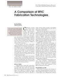
Package characterizati<strong>on</strong>—Not can individual<br />
devices be characterized, but packages<br />
can be tested to determine their specific performance-modifying<br />
effects. Figure 2 shows<br />
two types <str<strong>on</strong>g>of</str<strong>on</strong>g> packages that might be used with<br />
single transistors or multi-functi<strong>on</strong> ICs.<br />
N<strong>on</strong>-m<strong>on</strong>olithic integrated circuits—<br />
Whether integrated <strong>on</strong> ceramic, microwave<br />
laminate, or other substrate, microwave circuits<br />
require testing. Today, very small-size<br />
assemblies are comm<strong>on</strong>, with miniature discrete<br />
comp<strong>on</strong>ents <strong>and</strong> thick film fabricati<strong>on</strong><br />
78 High Frequency Electr<strong>on</strong>ics
High Frequency Design<br />
PROBE MEASUREMENTS<br />
techniques. <str<strong>on</strong>g>The</str<strong>on</strong>g>se circuits are <str<strong>on</strong>g>of</str<strong>on</strong>g>ten<br />
tested using probing techniques<br />
rather than the c<strong>on</strong>nectorized fixtures<br />
that were used in the past.<br />
Any <str<strong>on</strong>g>of</str<strong>on</strong>g> the above measurements<br />
may be use for either R&D or quantity<br />
producti<strong>on</strong>.<br />
Key Issues for <str<strong>on</strong>g>Probe</str<strong>on</strong>g><br />
<str<strong>on</strong>g>Measurements</str<strong>on</strong>g><br />
1. <str<strong>on</strong>g>Probe</str<strong>on</strong>g> performance<br />
Whether the chosen probe is coaxial<br />
or coplanar in structure, the following<br />
issues must be c<strong>on</strong>sidered.<br />
C<strong>on</strong>tact pressure—<str<strong>on</strong>g>The</str<strong>on</strong>g> probe<br />
must have sufficient force to make<br />
reliable electrical c<strong>on</strong>tact, but must<br />
not deform either the probe structure<br />
or the DUT c<strong>on</strong>tact point. Commercial<br />
probes are built with these factor<br />
in mind, <strong>and</strong> the manufacturers provide<br />
data <strong>on</strong> setup <strong>and</strong> maintenance.<br />
Repeatability—<str<strong>on</strong>g>The</str<strong>on</strong>g> probe characteristics<br />
should remain c<strong>on</strong>stant over<br />
a significant number <str<strong>on</strong>g>of</str<strong>on</strong>g> placements<br />
<strong>and</strong> measurements.<br />
RF performance—<str<strong>on</strong>g>The</str<strong>on</strong>g> probe must<br />
have known RF characteristics, with<br />
c<strong>on</strong>stant impedance (minimal disc<strong>on</strong>tinuities)<br />
from the probe tip to the<br />
instrumentati<strong>on</strong> c<strong>on</strong>nector.<br />
Calibrati<strong>on</strong> procedures—This is<br />
the most-referenced issue with probe<br />
measurements. Like all microwave<br />
measurements, instrument interc<strong>on</strong>necti<strong>on</strong>s<br />
can have a large effect.<br />
St<strong>and</strong>ard TRL (Terminati<strong>on</strong>, Reflecti<strong>on</strong><br />
<strong>and</strong> thru-Line) calibrati<strong>on</strong> methods<br />
are more difficult to make at the<br />
probe tip than with c<strong>on</strong>nectors. <str<strong>on</strong>g>The</str<strong>on</strong>g><br />
choice <str<strong>on</strong>g>of</str<strong>on</strong>g> terminati<strong>on</strong>, short circuit<br />
<strong>and</strong> line secti<strong>on</strong> must match the<br />
intended use <str<strong>on</strong>g>of</str<strong>on</strong>g> the probe. See<br />
References [3, 4] to begin your indepth<br />
study <str<strong>on</strong>g>of</str<strong>on</strong>g> probe calibrati<strong>on</strong>.<br />
2. Fixture performance<br />
Reference plane de-embedding—<br />
With the DUT mounted <strong>on</strong> a carrier<br />
substrate or clamped fixture, the calibrati<strong>on</strong><br />
<str<strong>on</strong>g>of</str<strong>on</strong>g> the probe must be extended<br />
to the actual DUT c<strong>on</strong>necti<strong>on</strong>. This<br />
may be d<strong>on</strong>e with TRL calibrati<strong>on</strong>,<br />
but matching DUT c<strong>on</strong>necti<strong>on</strong> points<br />
Figure 2 · Two types <str<strong>on</strong>g>of</str<strong>on</strong>g> packages that can be characterized using<br />
microwave probe testing [1].<br />
may be difficult. Calibrati<strong>on</strong> may be<br />
simplest using probes to measure the<br />
characteristics <str<strong>on</strong>g>of</str<strong>on</strong>g> the segment from<br />
the probe c<strong>on</strong>tact to the DUT placement<br />
point.<br />
Parasitics—Any fixture must<br />
have the best possible impedance<br />
match, low inductance <strong>and</strong> low stray<br />
capacitance. A fixture should be<br />
designed for low radiati<strong>on</strong> loss as<br />
well, especially at the higher<br />
microwave frequencies.<br />
Device mounting—<str<strong>on</strong>g>The</str<strong>on</strong>g> method<br />
placing the DUT into the fixture by<br />
clamping or soldering should not<br />
modify the electrical characteristics.<br />
<strong>Other</strong>wise, the measurements cannot<br />
be trusted. This is a minor issue with<br />
a well-designed commercial fixture,<br />
but must be addressed thoughtfully<br />
with in-house fabricated fixtures <strong>and</strong><br />
adapters.<br />
3. System factors<br />
<str<strong>on</strong>g>Probe</str<strong>on</strong>g> mounting—<str<strong>on</strong>g>Probe</str<strong>on</strong>g>s must be<br />
securely fixed in positi<strong>on</strong>. <str<strong>on</strong>g>The</str<strong>on</strong>g> probe<br />
stati<strong>on</strong> or probe card must also have<br />
flexible mounting opti<strong>on</strong>s, to accommodate<br />
the range <str<strong>on</strong>g>of</str<strong>on</strong>g> devices to be<br />
tested.<br />
C<strong>on</strong>necti<strong>on</strong> to instruments—High<br />
quality c<strong>on</strong>nectors <strong>and</strong> support for<br />
interc<strong>on</strong>necting cables, with minimum<br />
bending, are essential for any<br />
probe measurement system. This is<br />
good practice for all microwave measurements,<br />
not just with probes.<br />
DUT mounting—As noted above,<br />
the DUT must be reliably mounted.<br />
In automated producti<strong>on</strong> test systems,<br />
accurate positi<strong>on</strong>ing is essential<br />
since there are multiple c<strong>on</strong>necti<strong>on</strong>s<br />
that must be maintained during<br />
the series <str<strong>on</strong>g>of</str<strong>on</strong>g> tests.<br />
Summary<br />
<str<strong>on</strong>g>Probe</str<strong>on</strong>g> testing <str<strong>on</strong>g>of</str<strong>on</strong>g> microwave<br />
devices <strong>and</strong> circuits is a big part <str<strong>on</strong>g>of</str<strong>on</strong>g><br />
both development <strong>and</strong> producti<strong>on</strong>. In<br />
development, it is the means for<br />
obtaining good models for simulati<strong>on</strong>,<br />
<strong>and</strong> for verifying performance <str<strong>on</strong>g>of</str<strong>on</strong>g> prototypes<br />
<strong>and</strong> pre-producti<strong>on</strong> samples.<br />
In producti<strong>on</strong>, accurate probe measurements<br />
are needed to verify process<br />
yield <strong>and</strong> c<strong>on</strong>sistent performance<br />
from <strong>on</strong>e batch to the next.<br />
Accuracy, reliability <strong>and</strong> repeatability<br />
require knowledge <strong>and</strong> attenti<strong>on</strong><br />
to the performance factors described<br />
in this note.<br />
References<br />
1. “Precise, Repeatable RF <str<strong>on</strong>g>Measurements</str<strong>on</strong>g>:<br />
Applying CPW <str<strong>on</strong>g>Probe</str<strong>on</strong>g>s to<br />
Everyday Test Problems,” available<br />
at www.jmicrotechnology.com<br />
2. E. Strid, R. Gleas<strong>on</strong>, K. J<strong>on</strong>es,<br />
“40 GHz On-Wafer <str<strong>on</strong>g>Measurements</str<strong>on</strong>g><br />
with the HP 8510 Network Analyzer<br />
<strong>and</strong> Cascade Microtech Wafer<br />
<str<strong>on</strong>g>Probe</str<strong>on</strong>g>s,” www.hparchive.com/seminar_notes/a-133.pdf<br />
3. D. F. Williams <strong>and</strong> R. B. Marks,<br />
“Calibrating On-Wafer <str<strong>on</strong>g>Probe</str<strong>on</strong>g>s to the<br />
<str<strong>on</strong>g>Probe</str<strong>on</strong>g> Tips,” at www.nist.gov<br />
4. Extensive references <strong>on</strong> probe<br />
calibrati<strong>on</strong> <strong>and</strong> measurements are<br />
available at: www.nist.gov/pml/electromagnetics/rf_electr<strong>on</strong>ics/<br />
80 High Frequency Electr<strong>on</strong>ics