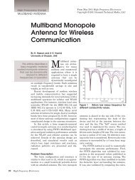
Line Diode Phase Shifters Part 2 - High Frequency Electronics
Line Diode Phase Shifters Part 2 - High Frequency Electronics
Line Diode Phase Shifters Part 2 - High Frequency Electronics

Create successful ePaper yourself
Turn your PDF publications into a flip-book with our unique Google optimized e-Paper software.
<strong>High</strong> <strong>Frequency</strong> Design<br />
PHASE SHIFTERS<br />
From May 2010 <strong>High</strong> <strong>Frequency</strong> <strong>Electronics</strong><br />
Copyright © 2010 Summit Technical Media, LLC<br />
Electrically Tunable Switched-<br />
<strong>Line</strong> <strong>Diode</strong> <strong>Phase</strong> <strong>Shifters</strong><br />
<strong>Part</strong> 2: Multi-Section Circuits<br />
By Leo G. Maloratsky<br />
Aerospace <strong>Electronics</strong> Co.<br />
Multibit switched<br />
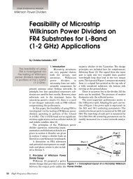
This article concludes the<br />
line phase<br />
author’s discussion of issues<br />
shifters [3, 10]<br />
that determine the circuit can be used to vary the<br />
configuration and construction<br />
method of switched-<br />
Digital phase shifters<br />
phase shift up to 360°.<br />
line phase shifters. provide a discrete set of<br />
phase states that are controlled<br />
by two-state “phase bits.” The number<br />
of binary weighted phase shifting “bits” can be<br />
cascaded to realize a variable phase shifter<br />
covering the desired range. Typically, the<br />
phase shifters are placed in tandem, with progressively<br />
greater phase shift angles to provide<br />
phase angle selectivity. Each switched<br />
delay line comprises a plurality of fixed time<br />
delays, which are combined to produce successive<br />
increments of delay in response to binary<br />
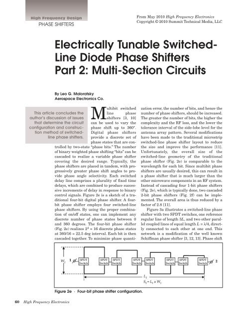
control signals. Figure 2e is a sketch of a traditional<br />
four-bit digital phase shifter. A fourbit<br />
phase shifter employs four switched-line<br />
phase shifters. By using the proper combination<br />
of on/off states, one can implement any<br />
discrete number of phase states between 0<br />
and 360 degrees. The four-bit phase shifter<br />
(Fig. 2e) realizes 2 4 = 16 discrete phase states<br />
at 360/16 = 22.5 deg interval. Each bit is then<br />
cascaded together. To minimize phase quantization<br />
error, the number of bits, and hence the<br />
number of phase shifters, should be increased.<br />
The greater the number of bits, the higher the<br />
complexity and the RF loss, and the lower the<br />
tolerance interval of the side-lobe level for the<br />
antenna array pattern. Several modifications<br />
have been made to the traditional microstrip<br />
switched-line phase shifter layout to reduce<br />
the size and improve the performance [11].<br />
Unfortunately, the overall size of the<br />
switched-line geometry of the traditional<br />
phase shifter (Fig. 2e) is comparable to the<br />
wavelength for each bit. Since multibit phase<br />
shifters are usually desired, this can result in<br />
a phase shifter that is much larger than the<br />
other microwave components in an RF system.<br />
Instead of cascading four 1-bit phase shifters<br />
(Fig. 2e), which is typically done, two cascaded<br />
2-bit phase shifters (Fig. 2f) can be implemented.<br />
The overall area is thus reduced by a<br />
factor of 2.8 [11].<br />
Figure 3a illustrates a switched-line phase<br />
shifter with two SPDT switches, one reference<br />
regular line of length 3L, and two other parallel<br />
coupled lines of equal length L = λ/4, directly<br />
connected to each other at one end. This<br />
network is a modification of the well known<br />
Schiffman phase shifter [3, 12, 13]. <strong>Phase</strong> shift<br />
Figure 2e · Four-bit phase shifter configuration.<br />
60 <strong>High</strong> <strong>Frequency</strong> <strong>Electronics</strong>
<strong>High</strong> <strong>Frequency</strong> Design<br />
PHASE SHIFTERS<br />
Figure 2f · Four-bit phase shifter configuration using<br />
two two-bit phase shifters.<br />
function is determined by the phase difference of signals<br />
transmitted through the coupled section of length L and<br />
the reference line of length 3L. The phase shift of the coupled-line<br />
section is determined by [3]<br />
cos<br />
⎛ z<br />
0e<br />
⎝<br />
⎜ z0<br />
o<br />
ϕ 1<br />
=<br />
⎛ z<br />
⎝<br />
⎜ z<br />
0e<br />
0o<br />
⎞<br />
2<br />
tan<br />
⎠<br />
⎟ − Θ<br />
⎞<br />
2<br />
tan<br />
⎠<br />
⎟ + Θ<br />
where Θ =2πl/λ is electrical length of the coupled-line<br />
section; z 0e<br />
and z 0o<br />
are even-mode and odd-mode<br />
impedances, respectively.<br />
The scattering matrix coefficients of the coupled line<br />
section are:<br />
S<br />
where<br />
( )<br />
2 2<br />
r − p + 1 sin 2Θ<br />
S11 = S22<br />
= −i<br />
2 ρcos<br />
2Θ+<br />
r isin<br />
2Θ<br />
1 r<br />
( )<br />
( ) + − +<br />
2 r cos 2Θ<br />
+ ρ<br />
= S =<br />
2 ρcos<br />
2Θ+<br />
r isin<br />
2Θ<br />
1 r<br />
2 2<br />
( ρ )<br />
( ) + − +<br />
( ρ )<br />
12 21 2 2<br />
r =<br />
z + z z − z<br />
, ρ =<br />
2 2<br />
0e 0o 0e 0o<br />
The matching condition (S 11<br />
= 0) for the coupled-lines<br />
section is<br />
z = z × z<br />
0 0e<br />
0o<br />
where z 0<br />
is the characteristic impedance of the coupled<br />
section.<br />
Figure 3 · Switched-line phase shifter with regular and<br />
coupled line sections, which maintains nearly constant<br />
phase shift over an octave bandwidth.<br />
62 <strong>High</strong> <strong>Frequency</strong> <strong>Electronics</strong>
<strong>High</strong> <strong>Frequency</strong> Design<br />
PHASE SHIFTERS<br />
Figure 4 · Switched-line phase shifter with regular and<br />
irregular line sections.<br />
The coupling coefficient for the mid-band operating frequency<br />
is<br />
pling allows for the small length of the irregular lines.<br />
Figure 4 illustrates a circuit where the output port of the<br />
first coupled conductor is electrically connected to the<br />
diagonal end of the second coupled conductor and DC-coupled<br />
to ground. The segment providing the diagonal connection<br />
should be as short as possible. The RF ground has<br />
to be apart from the irregular line and close to the appropriate<br />
input/output lines, that is, there should be no RF<br />
ground plane in the area of coupled conductors. The electrical<br />
length of the irregular lines is equal to the electrical<br />
length of the regular line. The physical length of the irregular<br />
lines l i<br />
= (0.02...0.08)λ i<br />
depends on the coefficient of<br />
magnetic coupling k m<br />
. In Figure 4, regular and irregular<br />
lines are printed on a thin Kapton substrate [3], which is<br />
connected to the base dielectric substrate Duroid 5880. At<br />
40% frequency band, this phase shifter provides a phase<br />
shift equal to 180° ±5°.<br />
Figure 5 illustrates different configurations of the<br />
reflection-type phase shifter. In the phase shifter shown<br />
in Figure 5a, the two output ports are terminated with<br />
voltage variable capacitors to ground. The divider splits<br />
the input signal of equal amplitude with a phase difference<br />
of 90°. Then the signals are reflected from capacitors<br />
back to the hybrid and combined at the output port 2. If<br />
the magnitudes and the angles of reflection signals are<br />
equal, there will be two reflection signals that are equal<br />
in amplitude and phase quadrature. These signals will<br />
combine at the isolated port 2 and cancel at the input port<br />
1. This reflection-type phase shifter provides a voltage<br />
variable phase shift of between 0° and close to –180°. The<br />
power divider including the two-branch hybrid and two<br />
reflected loads with shunt diodes D1 and D2 is shown in<br />
Figure 5b [15]. An input signal is divided by the quadrature<br />
divider among the two ports of the hybrid. The diodes<br />
are biased in the same state (forward or reverse biased).<br />
The input signal is divided into two quadrature components<br />
with equal amplitudes on the output ports. Turning<br />
the diodes ON or OFF changes the total path length for<br />
both reflected waves by Δϕ, producing a phase shift of Δϕ<br />
at output 2.<br />
The structure provides a wide bandwidth, depending<br />
on the bandwidth of the quadrature hybrid itself. Figure<br />
5c illustrates a reflection-type phase shifter which uses a<br />
divider/combiner based on the Lange coupler and varactor<br />
diodes D1 and D2. The ideal varactor diode is a variable<br />
capacitor with capacitance changing as a function of<br />
the DC bias. Capacitance can be controlled as a function<br />
of the reverse voltage applied to the PIN junction. The<br />
input signal is divided by the coupler and directed to two<br />
branches that are terminated with varactor diodes D1<br />
and D2, changing the phase of each signal equally. The<br />
reflected signals are then re-combined and are in phase at<br />
the output port. The reflected signals at the input port are<br />
out of phase and cancel each other. The phase shift pro-<br />
z<br />
k =<br />
z<br />
− z<br />
+ z<br />
0e<br />
0o<br />
0e<br />
0o<br />
In the octave band, this section provides a nearly constant<br />
phase shift Δϕ = 90° with respect to the regular line<br />
with electrical length 3Θ (see Fig. 3b). For z 0e<br />
/ z 0o<br />
, phase<br />
shift is equal 90° within ±4.8° for frequency ratio 2.27:1.<br />
For multi-octave operation, the plurality of sections interconnected<br />
in a cascade can be used (see Fig. 3c). It is a cascade<br />
of coupled sections of equal lengths (one quarterwavelength<br />
at the center operating frequency) and different<br />
coupling coefficients (k 1<br />
≠ k 2<br />
≠ k 3<br />
≠ k 4<br />
) [14].<br />
Print transmission lines in phase shifters can be classified<br />
as regular or irregular [3]. The term “irregular line”<br />
will stand for coupled conductors with strong magnetic<br />
coupling, with minimum influence of the RF ground plane<br />
on the parameters of the line (ideally, the absence of<br />
ground plane in the coupling area). Strong magnetic coupling<br />
is realized without magnets or ferrites [3]. Figure 4<br />
shows a switched-line phase shifter which includes a regular<br />
reference line and an irregular line. The irregular line<br />
[3, 15] includes coupled conductors with strong magnetic<br />
coupling which is realized without magnets or ferrites. In<br />
irregular lines, strong magnetic coupling between the<br />
lines provides for miniature dimensions and an increased<br />
bandwidth [3]. This coupling is characterized by the coefficient<br />
of magnetic coupling, k m<br />
. The strong magnetic cou-<br />
64 <strong>High</strong> <strong>Frequency</strong> <strong>Electronics</strong>
<strong>High</strong> <strong>Frequency</strong> Design<br />
PHASE SHIFTERS<br />
Figure 5 · Various configurations of reflection-type phase shifters.<br />
vided by this circuit is equal to the reflection phase shift<br />
provided by a single varactor. To decrease phase shifter<br />
insertion loss, GaAs varactor diodes with high Q-factor<br />
can be used. Varactors with higher tuning sensitivity provide<br />
a higher range of phase shift but have more amplitude<br />
variation. Varactors with lower tuning sensitivity<br />
and less phase control have lower loss and better amplitude<br />
linearity. Figure 5d illustrates the reflection-type<br />
phase shifter of the circulator type. The phase shift of this<br />
phase shifter is<br />
πΔ<br />
Δϕ<br />
= 2 l<br />
λ<br />
where Δl is twice the transmission line length. It has been<br />
reported by Garver [16] that a circulator having 20 dB<br />
isolation gives ±22.8° maximum phase error and 30 dB<br />
isolation gives ±7.2° maximum phase error.<br />
The switched-line reflection phase shifter (Fig. 5e) is<br />
based on reflect stubs (open-end transmission lines) that<br />
are switched using SP3T switches. Separation of incident<br />
and reflected signals is realized by quadrature hybrids<br />
[3], such as the 3-dB branch-line couplers or Lange couplers.<br />
The input signal is divided into two quadrature<br />
components with equal amplitudes on the output ports.<br />
These two signals are reflected from one of the three<br />
opened stubs and recombined in phase on the normally<br />
decoupled port.<br />
Practical phase shifter design faces three problems.<br />
One is associated with size, the second with insertion loss,<br />
and the third with cost. Selection of the type of phase<br />
shifter depends on system configuration and the RF<br />
power level. An ideal phase shifter should have low insertion<br />
loss, acceptable phase accuracy, and minimum amplitude<br />
variation. For an active antenna array, the accuracy<br />
of phase and size of the phase shifter are more critical<br />
than the insertion loss because the signal power is amplified<br />
after the phase shift. The design trade-offs for the<br />
phase shifters are insertion loss, balance between phase<br />
states, and phase accuracy. <strong>Phase</strong> shift linearity and max-<br />
66 <strong>High</strong> <strong>Frequency</strong> <strong>Electronics</strong>
<strong>High</strong> <strong>Frequency</strong> Design<br />
PHASE SHIFTERS<br />
imum value can be increased by utilizing the multi-section<br />
approach, but cost, size and insertion loss of this<br />
approach will be higher. Low cost PIN diodes have parasitic<br />
elements which adversely affect their performance.<br />
As a result, these diodes are far from ideal. In the digital<br />
design, as total phase shift increases, total accuracy generally<br />
decreases. This results from the cumulative effect<br />
of multiple internal reflections in the unit. Larger phase<br />
shifts tend to require more elements, which in turn leads<br />
to higher cost and complexity. While the differential<br />
phase shift tends to be broadband, it can be difficult to<br />
balance the insertion loss between the states.<br />
References<br />
1. Koul, K. S. and Bhat, B., Microwave and Millimeter<br />
Wave <strong>Phase</strong> <strong>Shifters</strong>, Vol II: Semiconductor and Delay<br />
<strong>Line</strong> <strong>Phase</strong> <strong>Shifters</strong>, Artech House, 1991.<br />
2. Pozar, D. M., Microwave Engineering, 2nd Edition,<br />
John Wiley & Sons, 1998.<br />
3. Maloratsky, L. G., Passive RF & Microwave<br />
Integrated Circuits, Elsevier, 2003.<br />
4. Watson, T., “Affordable <strong>Phase</strong> <strong>Shifters</strong> for<br />
Electronically Scanned <strong>Phase</strong> Array Antennas,” RF<br />
Design, October 2003, pp. 42, 44, 46, 48.<br />
5. Maloratsky, L. G., “Switched Directional/Omnidirectional<br />
Antenna Module for Amplitude Monopulse<br />
Systems,” IEEE Antennas and Propagation Magazine,”<br />
December, 2008.<br />
6. Maloratsky, L. G., et al. “Switched Beam Forming<br />
Network for an Amplitude Monopulse Directional and<br />
Omnidirectional Antenna,” U.S. Pat. No. 7,508,343, March<br />
24, 2009.<br />
7. Maloratsky, L. G., “Setting Strategies for Printed<br />
Transmission <strong>Line</strong>s,” Microwaves & RF, September 2008,<br />
pp. 100-112.<br />
8. Maloratsky, L. G., “Setting Strategies for Planar<br />
Directional Couplers,” Microwaves & RF, December 2009.<br />
9. Maloratsky, L. G. “Setting Strategy for Planar<br />
Dividers/Combiners,” Microwaves & RF, December 2009.<br />
10. G.-L. Tan, at., “Low-loss 2- and 4-bit TTD MEMS<br />
<strong>Phase</strong> <strong>Shifters</strong> Based on SP4T Switches,” IEEE Trans.<br />
Microw. Theory Tech., pt. 2, Vol. 51, No. 1, pp. 297-304,<br />
Jan. 2003.<br />
11. Bairavasubramanian, R., et al., “Recent<br />
Developments on Lightweight, Flexible, Dual Polarization/<strong>Frequency</strong><br />
<strong>Phase</strong>d Arrays Using RF MEMS Switches<br />
on LCP Multilayer Substrates for Remote Sensing of<br />
Precipitation,” Georgia Institute of Technology, School of<br />
Electrical and Computer Engineering, 2006.<br />
12. Schiffman, B. M., “A New Class of Broadband
Microwave 90-Degree <strong>Phase</strong> <strong>Shifters</strong>,” IRE Trans.<br />
Microwave Theory Tech., Vol. MTT-6, April 1958, pp. 232-<br />
237.<br />
13. Schiffman, B. M., “Multisection Microwave <strong>Phase</strong><br />
Shift Network,” IEEE Trans. Microwave Theory Tech., Vol.<br />
MTT-14, April 1966, p. 209.<br />
14. Meschanov, V. P., et. al., “A New Structure of<br />
Microwave Ultrawide-Band Differential <strong>Phase</strong> Shifter,”<br />
IEEE Trans. Microwave Theory Tech., Vol.42, No.5, May<br />
1994, pp. 762-765.<br />
15. Maloratsky, L. G., “Design Regular- and Irregular-<br />
Print Coupler <strong>Line</strong>s,” Microwaves & RF, September 2000,<br />
pp. 97-106.<br />
16. Garver, R. V., Microwave Control Devices, Dedham,<br />
MA: Artech House, 1978.<br />
Author Information<br />
Leo G. Maloratsky received his MSEE degree from the<br />
Moscow Aviation Institute and his PhD from the Moscow<br />
Institute of Communications in 1962 and 1967, respectively.<br />
Since 1962, he has involved in the research, development<br />
and production of RF and microwave integrated<br />
circuits at the Electrotechnical Institute, and he was<br />
assistant professor at the Moscow Institute of<br />
Radioelectronics. From 1992 to 1997, he was a staff engineer<br />
at Allied Signal. From 1997 to 2008, he was a principal<br />
engineer at Rockwell Collins where he worked on RF<br />
and microwave integrated circuits for avionics systems.<br />
Since 2008 he joined Aerospace <strong>Electronics</strong> Co. He is<br />
author of four monographs, one textbook, over 50 articles,<br />
and 20 patents. His latest book is Passive RF and<br />
Microwave Integrated Circuits, 2004, Elsevier. He is listed<br />
in the encyclopedias Who is Who in the World, Who is Who<br />
in America, and 2000 Outstanding Scientists. Dr.<br />
Maloratsky my be contacted at: lmaloratsky@cfl.rr.com<br />
Authors Wanted<br />
<strong>High</strong> <strong>Frequency</strong> <strong>Electronics</strong> has an ongoing need for<br />
contributed technical articles. Engineers working in<br />
high frequency/high speed design are developing a<br />
vast array of applications and have varying levels of<br />
education and experience. Almost any topic related<br />
to this specialty area will be considered—at technical<br />
levels ranging from a basic tutorial review to<br />
advanced design methods and in-depth theory.<br />
Our authors report useful reader feedback, and all<br />
articles are maintained for download in our Archives.<br />
Send an idea, abstract or completed manuscript to:<br />
Gary Breed, Editorial Director<br />
gary@highfrequencyelectronics.com