New LDMOS Model Delivers Powerful Transistor Libraryâ Part 1 ...
New LDMOS Model Delivers Powerful Transistor Libraryâ Part 1 ...
New LDMOS Model Delivers Powerful Transistor Libraryâ Part 1 ...

You also want an ePaper? Increase the reach of your titles
YUMPU automatically turns print PDFs into web optimized ePapers that Google loves.
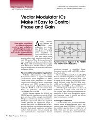
High Frequency Design<br />
<strong>LDMOS</strong> MODEL<br />
substrate loss circuit, consisting of a<br />
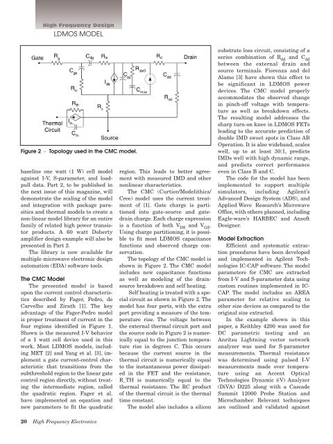
Figure 2 · Topology used in the CMC model.<br />
baseline one watt (1 W) cell model<br />
against I-V, S-parameter, and loadpull<br />
data. <strong>Part</strong> 2, to be published in<br />
the next issue of this magazine, will<br />
demonstrate the scaling of the model<br />
and integration with package parasitics<br />
and thermal models to create a<br />
non-linear model library for an entire<br />
family of related high power transistor<br />
products. A 60 watt Doherty<br />
amplifier design example will also be<br />
presented in <strong>Part</strong> 2.<br />
The library is now available for<br />
multiple microwave electronic design<br />
automation (EDA) software tools.<br />
The CMC <strong>Model</strong><br />
The presented model is based<br />
upon the current control characteristics<br />
described by Fager, Pedro, de<br />
Carvelho and Zirath [1]. The key<br />
advantage of the Fager-Pedro model<br />
is proper treatment of current in the<br />
four regions identified in Figure 1.<br />
Shown is the measured I-V behavior<br />
of a 1 watt cell device used in this<br />
work. Most <strong>LDMOS</strong> models, including<br />
MET [2] and Yang et al. [3], implement<br />
a gate current-control characteristic<br />
that transitions from the<br />
subthreshold region to the linear gate<br />
control region directly, without treating<br />
the intermediate region, called<br />
the quadratic region. Fager et al.<br />
have implemented an equation and<br />
new parameters to fit the quadratic<br />
region. This leads to better agreement<br />
with measured IMD and other<br />
nonlinear characteristics.<br />
The CMC (Curtice/<strong>Model</strong>ithics/<br />
Cree) model uses the current treatment<br />
of [1]. Gate charge is partitioned<br />
into gate-source and gatedrain<br />
charge. Each charge expression<br />
is a function of both V DS<br />
and V GS<br />
.<br />
Using charge partitioning, it is possible<br />
to fit most <strong>LDMOS</strong> capacitance<br />
functions and observed charge conservation.<br />
The topology of the CMC model is<br />
shown in Figure 2. The CMC model<br />
includes new capacitance functions<br />
as well as modeling of the drainsource<br />
breakdown and self heating.<br />
Self heating is treated with a special<br />
circuit as shown in Figure 2. The<br />
model has four ports, with the extra<br />
port providing a measure of the temperature<br />
rise. The voltage between<br />
the external thermal circuit port and<br />
the source node in Figure 2 is numerically<br />
equal to the junction temperature<br />
rise in degrees C. This occurs<br />
because the current source in the<br />
thermal circuit is numerically equal<br />
to the instantaneous power dissipated<br />
in the FET and the resistance,<br />
R_TH is numerically equal to the<br />
thermal resistance. The RC product<br />
of the thermal circuit is the thermal<br />
time constant.<br />
The model also includes a silicon<br />
series combination of R dd<br />
and C dd<br />
between the external drain and<br />
source terminals. Fiorenza and del<br />
Alamo [3] have shown this effect to<br />
be significant in <strong>LDMOS</strong> power<br />
devices. The CMC model properly<br />
accommodates the observed change<br />
in pinch-off voltage with temperature<br />
as well as breakdown effects.<br />
The resulting model addresses the<br />
sharp turn-on knee in <strong>LDMOS</strong> FETs<br />
leading to the accurate prediction of<br />
double IMD sweet spots in Class AB<br />
Operation. It is also wideband, scales<br />
well, up to at least 30:1, predicts<br />
IMDs well with high dynamic range,<br />
and predicts correct performance<br />
even in Class B and C.<br />
The code for the model has been<br />
implemented to support multiple<br />
simulators, including Agilent’s<br />
Advanced Design System (ADS), and<br />
Applied Wave Research’s Microwave<br />
Office, with others planned, including<br />
Eagle-ware’s HARBEC and Ansoft<br />
Designer.<br />
<strong>Model</strong> Extraction<br />
Efficient and systematic extraction<br />
procedures have been developed<br />
and implemented in Agilent Technologies<br />
IC-CAP software. The model<br />
parameters for CMC are extracted<br />
from I-V and S-parameter data using<br />
custom routines implemented in IC-<br />
CAP. The model includes an AREA<br />
parameter for relative scaling to<br />
other size devices as compared to the<br />
original size extracted.<br />
In the example shown in this<br />
paper, a Keithley 4200 was used for<br />
DC parametric testing and an<br />
Anritsu Lightning vector network<br />
analyzer was used for S-parameter<br />
measurements. Thermal resistance<br />
was determined using pulsed I-V<br />
measurements made over temperature<br />
using an Accent Optical<br />
Technologies Dynamic i(V) Analyzer<br />
(DiVA) D225 along with a Cascade<br />
Summit 12000 Probe Station and<br />
Microchamber. Relevant techniques<br />
are outlined and validated against<br />
20 High Frequency Electronics