Multiband Monopole Antenna for Wireless Communication
Multiband Monopole Antenna for Wireless Communication
Multiband Monopole Antenna for Wireless Communication

You also want an ePaper? Increase the reach of your titles
YUMPU automatically turns print PDFs into web optimized ePapers that Google loves.
High Frequency Design<br />
MULTIBAND ANTENNA<br />
From May 2011 High Frequency Electronics<br />
Copyright © 2011 Summit Technical Media, LLC<br />
<strong>Multiband</strong> <strong>Monopole</strong><br />
<strong>Antenna</strong> <strong>for</strong> <strong>Wireless</strong><br />
<strong>Communication</strong><br />
By H. Hassan and A-K. Hamid<br />
University of Sharjah, UAE<br />
<strong>Multiband</strong> antennas<br />
are attrac-<br />
This article describes a<br />
lossy magnetic-material<br />
tive <strong>for</strong> many<br />
coated monopole antenna military and commercial<br />
that can be dynamically applications where it is<br />
retuned to different required to have a single<br />
frequencies of operation antenna that can be<br />
dynamically reconfigured<br />
on multiple frequency bands. Such antennas<br />
result in considerable savings in size and<br />
weight, as well as cost.<br />
Recent development of modern wireless<br />
and mobile communication has suggested<br />
increasing demands <strong>for</strong> novel antennas with a<br />
multiband operation <strong>for</strong> cellular and WLAN<br />
applications. For instance, wireless local area<br />
networks (WLAN) <strong>for</strong> the IEEE 802.11b and<br />
IEEE 802.11a operate in 2.4-2.48 GHz, 5.15-<br />
5.35 GHz and 5.725-5.825 GHz. Many novel<br />
antenna structures <strong>for</strong> single, dual or multiple<br />
bands have been proposed by [2-16], however,<br />
most of these antenna configurations suggest<br />
complicated design in the antenna structures.<br />
In this article, a lossy magnetic-material<br />
coated monopole antenna on a conducting box<br />
is simulated by using FDTD. <strong>Multiband</strong> operation<br />
and good radiation per<strong>for</strong>mance suitable<br />
<strong>for</strong> the WLAN and cellular systems can be<br />
achieved. Details of the antenna design are<br />
described, and simulated results such as<br />
return loss, input resistance and reactance,<br />
radiation patterns are presented and discussed.<br />
Problem Description<br />
The basic configuration and structure is<br />
similar to that used in [1], which is an approximation<br />
to a small hand-held portable device<br />
with an attached antenna. The wire monopole<br />
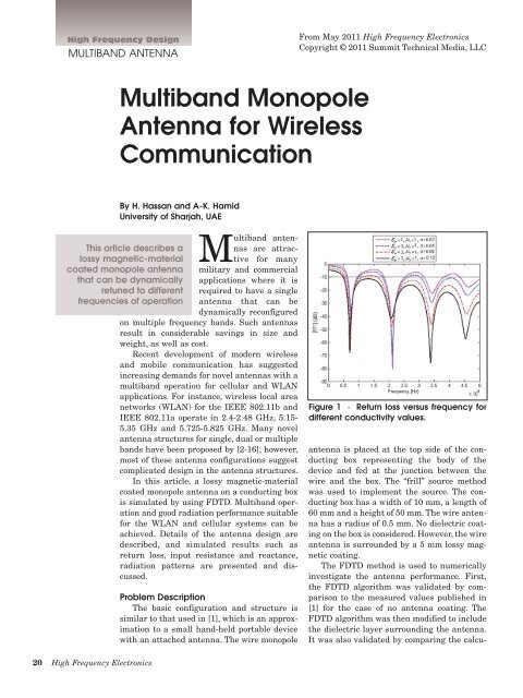
Figure 1 · Return loss versus frequency <strong>for</strong><br />
different conductivity values.<br />
antenna is placed at the top side of the conducting<br />
box representing the body of the<br />
device and fed at the junction between the<br />
wire and the box. The “frill” source method<br />
was used to implement the source. The conducting<br />
box has a width of 10 mm, a length of<br />
60 mm and a height of 50 mm. The wire antenna<br />
has a radius of 0.5 mm. No dielectric coating<br />
on the box is considered. However, the wire<br />
antenna is surrounded by a 5 mm lossy magnetic<br />
coating.<br />
The FDTD method is used to numerically<br />
investigate the antenna per<strong>for</strong>mance. First,<br />
the FDTD algorithm was validated by comparison<br />
to the measured values published in<br />
[1] <strong>for</strong> the case of no antenna coating. The<br />
FDTD algorithm was then modified to include<br />
the dielectric layer surrounding the antenna.<br />
It was also validated by comparing the calcu-<br />
20 High Frequency Electronics
High Frequency Design<br />
MULTIBAND ANTENNA<br />
Figure 2 · Return loss versus σ at f = 1.5 GHz and f =<br />
5 GHz.<br />
Figure 3 · The input reactance versus frequency at various<br />
values of σ.<br />
Figure 5 · The input reactance versus frequency <strong>for</strong> µ r<br />
values of 1 and 2.<br />
Figure 4 · The input resistance versus frequency at various<br />
values of σ.<br />
lated values published in <strong>for</strong> the case of changing permittivity<br />
while keeping the permeability unchanged [18].<br />
In the simulation, all sides of the computation domain<br />
were terminated by PML layers [19] to enhance the accuracy<br />
of the results [19]. The structure is excited by a<br />
Gaussian pulse to obtain results over a wide bandwidth.<br />
Numerical Results<br />
Several FDTD simulation runs were per<strong>for</strong>med <strong>for</strong> the<br />
characterization of the antenna per<strong>for</strong>mance. In Figure 1,<br />
the return loss versus frequency curves <strong>for</strong> various conductivity<br />
values are presented. From the given values, it<br />
can be noticed that the return loss decreases with<br />
increasing σ. This result is convincing because as we<br />
increase σ, the resistance will decrease and the lost power<br />
will also decrease. This creates an easy and simple way to<br />
enhance the reception conditions, while many recent<br />
papers try to enhance the reception conditions by implementing<br />
complicated antenna structures [3-6, 9-10].<br />
Figure 2 shows the return loss versus σ at a given frequency.<br />
For the given values, it can be seen that the<br />
return loss versus σ at frequency (1.5 GHz) is totally linear,<br />
however, <strong>for</strong> higher frequencies (i.e., 5 GHz), the magnitude<br />
of the return loss tends to be more exponantially<br />
decaying as we increase σ. Further, the return loss at<br />
higher frequencies seems to be lower than at lower frequencies.<br />
Figure 3 shows the simulated input reactance versus<br />
frequency <strong>for</strong> different conductivity values. It shows that<br />
increasing σ will decrease the input reactance values<br />
closer to zero, as a result, this will enable the device to<br />
operate on many center frequencies.<br />
Figure 4 shows the simulated input resistance versus<br />
frequency <strong>for</strong> different conductivity values. It can be seen<br />
that increasing σ, the input resistance tends to decrease<br />
to 50 Ω, which is the practical impdance of a coaxial cable.<br />
The antenna center frequency can be shifted to bands<br />
commonly used <strong>for</strong> practical applications in cellular or<br />
WLAN by changing the permeability of the antenna coating<br />
material.<br />
This case is presented in Figure 5, where the center<br />
frequency is changed from 2.3 to 2.6 GHz by increasing<br />
22 High Frequency Electronics
High Frequency Design<br />
MULTIBAND ANTENNA<br />
Figure 6 · (a) Simulation results of the E-plane radiation<br />
patterns of the antenna at 900 MHz <strong>for</strong> various values of<br />
σ. (b) Simulation results of the H-plane radiation patterns<br />
of the antenna at 900 MHz <strong>for</strong> various values of σ.<br />
the relative permeability of the coating from 1 to 2.<br />
Conclusions<br />
A study of the effects of lossy magnetic coating on a<br />
monopole antenna per<strong>for</strong>mance is presented. In particular,<br />
it has been shown that a monopole antenna can operate<br />
in multiband cellular and WLAN applications by<br />
changing the conductivity of the coating material with<br />
excellent radiation properties.<br />
Acknowledgments<br />
The authors wish to acknowledge the support provided<br />
by the University of Sharjah, U.A.E.<br />
References<br />
1. R. Luebbers, Li. Chen, T. Uno and S. Adachi. “FDTD<br />
calculation of radiation patterns, impedance, and gain <strong>for</strong><br />
a monopole antenna on a conducting box,” IEEE<br />
Transactions on <strong>Antenna</strong>s and Propagation, vol. 40, no.<br />
12, pp. 1577-1583. 1992.<br />
2. W. C. Liu, “Compact microstrip-line-fed ring<br />
monopole antenna with tuning strip <strong>for</strong> 5 GHz WLAN<br />
operation,” Electronics Letters, vol. 41, no. 15, pp. 831-832,<br />
2005.<br />
3. W. C. Liu, “Broadband dual-frequency meandered<br />
CPW-fed monopole antenna,” Electronics Letters, vol. 40,<br />
no.21, pp. 1319-1320, 2004.<br />
4. L. Zhang, Y.-C. Jiao, G. Zhao, Y. Song, and F.-S.<br />
Zhang, “Broadband dual-band CPW-fed closed rectangular<br />
ring monopole antenna with a vertical strip <strong>for</strong> WLAN<br />
operation,” Microwave and Optical Technology Letters,<br />
vol. 50, pp. 1929-1931, 2008.<br />
5. J. H.Yoon, “Fabrication and measurement of rectangular<br />
ring with opened CPW-fed monopole antenna <strong>for</strong><br />
2.4/5.2-GHz WLAN operation,” Microwave and Optical<br />
Technology Letters, vol. 48, pp. 1480-1483, 2006.<br />
6. R. K. Raj, M. Joseph, B. Paul, and P. Mohanan,<br />
“Compact planar multiband antenna <strong>for</strong> GPS, DCS,<br />
2.4/5.8 GHz WLAN applications,” Electronics Letters, vol.<br />
41, pp. 290-291, 2005.<br />
7. J. Y. Li, J. L. Guo, Y. B. Gan, and Q. Z. Liu, “The triband<br />
per<strong>for</strong>mance of sleeve dipole antenna,” Journal of<br />
Electromagnetic Waves and Applications, vol. 19, pp. 2081-<br />
2092, 2005.<br />
8. K. G. Thomas, and M. Sreenivasan, “A novel triple<br />
band printed antenna <strong>for</strong> WLAN/WiMAX applications,”<br />
Microwave and Optical Technology Letters, vol. 51, pp.<br />
2481-2485, 2009.<br />
9. H. Sabri and Z. Atlasbaf, “Two novel compact tripleband<br />
microstrip annular-ring slot antennas <strong>for</strong> pcs-1900<br />
and WLAN applications,” Progress In Electromagnetics<br />
Research Letters, vol. 5, pp. 87-98, 2008.<br />
10. Jia, J.-Y., C.-I. Hsu, and S.-C. Hsu, “Design of a<br />
compact dual-band annular-ring slot antenna,” IEEE<br />
<strong>Antenna</strong>s and <strong>Wireless</strong> Propagation Letters, vol. 6, pp.423-<br />
426, 2007.<br />
11. R. L. Li, G. DeJean, M. M. Tentzeris, and J. Laskar,<br />
“Novel multi-band broadband planar wire antennas <strong>for</strong><br />
wireless communication handheld terminals,” IEEE<br />
<strong>Antenna</strong>s and Propagation Society International<br />
Symposium, vol. 3, pp. 44-47, 2003.<br />
12. N. Behdadand, K. Sarabandi, “A compact dual/<br />
multi-band wireless LAN antenna,” IEEE <strong>Antenna</strong>s and<br />
Propagation Society International Symposium, vol. 2B,<br />
pp. 527-530, 2005.<br />
13. Y. Ryu, J.Park, et al., “Multi-band antenna using<br />
dual composite right/left handed transmission line,” IEEE<br />
<strong>Antenna</strong>s and Propagation Society International<br />
Symposium, pp. 1-4, 2008.<br />
14. R.L. Li, B. Pan, T. Wu, J. Laskar, M.M. Tentzeris, “A<br />
triple-band low-profile planar antenna <strong>for</strong> wireless appli-<br />
24 High Frequency Electronics
cations,” IEEE <strong>Antenna</strong>s and Propagation Society<br />
International Symposium, pp. 1-4, 2008<br />
15. Y.-L. Kuo, and K.-L. Wong, “Printed double-T<br />
monopole antenna <strong>for</strong> 2.4/5.2 GHz dual-band WLAN operations,”<br />
<strong>Antenna</strong>s and Propagation, IEEE Transactions,<br />
vol. 51, no .9, pp. 2187-2192, 2003.<br />
16. J. H. Kim, J. N. Lee, and J. K. Park, “Triple-band<br />
antenna with slots <strong>for</strong> PCS/WLAN/UWB applications,”<br />
Microwave and Optical Technology Letters, vol. 52, pp.<br />
2738-2741, 2009.<br />
17. H. Ebrahim Zadeh, Ch. Ghobadi and J. Nourinia,<br />
“Circular Multifractal UWB monopole antenna,” IEICE<br />
Electron. Express, vol. 7, no. 10, pp. 717-721, 2010.<br />
18. M. Alsunaidi, A. Hamid, “FDTD analysis of antenna<br />
coating effects on the per<strong>for</strong>mance of cellular phones,”<br />
IEEE <strong>Antenna</strong> and Propagation Society International<br />
Symposium, vol. 1, pp. 520-523,1998.<br />
19. J.P. Berenger, “A perfectly matched layer <strong>for</strong> the<br />
absorption of electromagnetic waves,” vol. 114, pp. 185-20,<br />
1994.<br />
Author In<strong>for</strong>mation<br />
H.Hamad was born in Dubai, UAE, on May 4, 1986.<br />
She received her B.Sc. degree in Electrical Engineering<br />
from University of Sharjah, Sharjah, UAE, in 2007. She is<br />
pursuing her M.Sc. degree in Electrical Engineering at<br />
the same university. Her research interests include FDTD<br />
simulation of cellular phones and micro-strip patch<br />
antennas<br />
A-K. Hamid was born in Tulkarm, West Bank, on Sept.<br />
9, 1963. He received the B.Sc. degree in Electrical<br />
Engineering from West Virginia Institute of Technology<br />
and University of West Virginia in 1985. He received the<br />
M.Sc. and Ph.D. degrees from the University of Manitoba,<br />
Winnipeg, Manitoba, Canada in 1988 and 1991, respectively,<br />
both in Electrical Engineering. From 1991-1993, he<br />
was with Quantic Laboratories Inc., Winnipeg, Manitoba,<br />
Canada, developing two and three dimensional electromagnetic<br />
field solvers using boundary integral method.<br />
From 1994-2000 he was with the faculty of electrical engineering<br />
at King Fahd University of Petroleum and<br />
Minerals, Dhahran, Saudi Arabia. Since Sept. 2000 he is<br />
with the department of electrical and computer engineering<br />
at the University of Sharjah, Sharjah, United Arab<br />
Emirates. His research interest includes EM wave scattering<br />
from two and three dimensional bodies, propagation<br />
along waveguides with discontinuities, FDTD simulation<br />
of cellular phones, and inverse scattering using<br />
neural networks. He can be reached by e-mail at:<br />
akhamid@sharjah.ac.ae<br />
May 2011 27