Petr SICHO - Helsinki Institute of Physics
Petr SICHO - Helsinki Institute of Physics
Petr SICHO - Helsinki Institute of Physics

You also want an ePaper? Increase the reach of your titles
YUMPU automatically turns print PDFs into web optimized ePapers that Google loves.
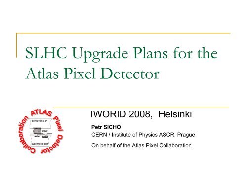
SLHC Upgrade Plans for the<br />
Atlas Pixel Detector<br />
IWORID 2008, <strong>Helsinki</strong><br />
<strong>Petr</strong> <strong>SICHO</strong><br />
CERN / <strong>Institute</strong> <strong>of</strong> <strong>Physics</strong> ASCR, Prague<br />
On behalf <strong>of</strong> the Atlas Pixel Collaboration
Pixel detector in the heart <strong>of</strong> Atlas<br />
Atlas Detector<br />
• Length 46m<br />
• Φ22m<br />
• 7000 tonnes<br />
• First beam injection<br />
in August 2008!<br />
Inner Detector <strong>of</strong> Atlas<br />
(7m long; Φ2,3m)<br />
• TRT<br />
• SCT<br />
• Pixels<br />
1/07/2007 IWORID2008, Helsinky 2
Pixel Package and the Pixel Detector<br />
Pixel package<br />
• Full length 7m,<br />
(includes services)<br />
SQP + Beam Pipe<br />
Support Structure<br />
Connection <strong>of</strong> cables<br />
and pipes (PP1)<br />
Pixel<br />
Detector<br />
SQP + Beam Pipe<br />
Support Structure<br />
Pixel detector<br />
• 3 barrel layers<br />
at R5, 9, 12cm from IP<br />
• 3 disks at each side<br />
• Tracking volume:<br />
1.6m long, 0.2m radius<br />
1.8m 2 <strong>of</strong> silicon in total<br />
• 1744 modules<br />
~ 80 millions channels<br />
• Good d 0 and z 0 resolution<br />
(12μm and 70μm) crucial for<br />
physics program<br />
• Use evaporative cooling to<br />
remove 10 kW <strong>of</strong> power and<br />
operating temperature ~ -5 o C<br />
1/07/2007 IWORID2008, Helsinky 3
Pixel module – basic element <strong>of</strong> Pixel Detector<br />
Pixel Module – short description:<br />
• Each module has 46080 pixels in<br />
an area <strong>of</strong> ~10 cm 2 (1.6 x 6 cm)<br />
• Sensors tile are arrays <strong>of</strong> pixel<br />
diodes (n+ on n substrate)<br />
• Pixel size is 50 x 400 μm<br />
• Silicon sensors bump-bonded to<br />
16 FE chips (~12 μm bumps)<br />
• FE chips are connected to one<br />
controller chip via wire bonding<br />
and flex hybrid<br />
• Micro-cable (~1m) connected to<br />
service patch panel (PP0<br />
connection)<br />
• Modules are placed on carbon<br />
fiber cooling/support structure<br />
• Data transmission trough optical<br />
links<br />
1/07/2007 IWORID2008, Helsinky 4
What is the implication for the Pixels at SLHC?<br />
What are Super Luminosity LHC highlights?<br />
• SLHC (√s ≈ 14 TeV, L ≈ 10 35 cm -2 s -1 ) would allow to extend significantly the LHC physics<br />
aims whilst keeping the same tunnel, machine dipoles and large part <strong>of</strong> “existing” detectors.<br />
• Integrated luminosity at SLHC will reach ~300 fb -1 per year!<br />
What are requirements for trackers?<br />
• Higher Granularity needed! Trackers need more channels to achieve the same<br />
performance with much higher occupancy. More channels - more power required.<br />
Expectation <strong>of</strong> 5-10ktracks/event, pile-up up to 400events / BC!<br />
• Trackers need improved radiation hardness for electronics and especially for sensors<br />
• Inner/forward parts <strong>of</strong> LHC detectors must be changed-hardened-upgraded<br />
‣ Electronics (FE chips)– to cope with very high data rate. Certainly more channels are<br />
needed (~2 x more) - pixel size must be significantly decreased, threshold must be<br />
further decreased !<br />
‣ Radiation hard sensors needed to survive at fluence well above 10 16 n eq /cm 2<br />
• Substantial R&Ds in many different areas are required<br />
• Simulation will play an important role in design definition<br />
Schedule?<br />
• LHC needs to do a major replacement <strong>of</strong> quadrupolest in interaction regions after an<br />
integrated luminosity <strong>of</strong> ~600 fb -1 (2016/2017)<br />
• Aggressive R&D schedule for tracker sub-detectors needed to fit 2016/2017 LHC shutdown<br />
schedule!<br />
1/07/2007 IWORID2008, Helsinky 5
LHC SLHC Luminosity upgrade scenario<br />
Lyn Evans, SLHC-PP kick-<strong>of</strong>f meeting, CERN 9 April 2008<br />
LHC/SLHC<br />
shutdown<br />
Existing B-layer nominal<br />
lifetime ~300 fb -1<br />
~2012-2013<br />
1/07/2007 IWORID2008, Helsinky 6
Which parts are concerned?<br />
• Detector Layout (overall ID layout)<br />
• Sensors<br />
• FE chips<br />
• Module architecture (low cost and reliable solution preferable)<br />
• Power scheme to be upgraded, keeping about the same amount <strong>of</strong><br />
recent services especially cables (serial powering?)<br />
• R/O Architecture<br />
• Optical links (higher data transmission speed)<br />
• DCS (dedicated stave DCS chip), reducing <strong>of</strong> DCS cables<br />
• Cooling (recently ~ -5degr.C, for SLHC tracker regions considered<br />
temperatures even up to -35degr.C)<br />
• Mechanics<br />
1/07/2007 IWORID2008, Helsinky 7
Layout studies - new layout <strong>of</strong> ID – Strawman<br />
Strawman 07<br />
4 Pixel<br />
3 Short Strips<br />
2 Long Strips<br />
Ref. Nigel Hessey<br />
“Strawman 07 numbers”<br />
Strawman 07 is reference ID layout to compare other<br />
options. The simulation and performance studies are<br />
still ongoing so geometrical changes are certainly<br />
considered!<br />
New version - Strawman 08 to be released soon<br />
1/07/2007 IWORID2008, Helsinky 8
Innermost Pixel B-physics layer replacement<br />
– intermediate step on the way to SLHC<br />
• LHC will increase substantially (~2x) its nominal luminosity even before upgrading to<br />
SLHC (scheduled to 2016)<br />
• The innermost pixel layer (B physics layer very probably would not survive with<br />
reasonable tracking efficiency until the LHC/SLHC upgrade (scheduled to 2016)<br />
• Present B layer is not designed for luminosities above L ≈ 2·10 34 cm -2 s -1 (granularity<br />
issue – deteriorating <strong>of</strong> efficiency is starting), stopping to work @ L ≈ 2·10 34 cm -2 s -1<br />
• Present B layer has to be replaced even before SLHC upgrade, probably during<br />
shutdown 2012 (6-8 months, new triplets and first injector to be upgraded)<br />
• Very limited time for substantial R&D!<br />
• Certainly there is not enough time to remove complete “pixel package” to surface<br />
large cool down time expected – human safety issues!<br />
• Very probably new additional B-layer has to be inserted together with new beam<br />
pipe <strong>of</strong> reduced size without removing pixels package out <strong>of</strong> Atlas<br />
• There are not yet final decisions concerning B-layer upgrade/replacement, expected<br />
in coming weeks ….<br />
1/07/2007 IWORID2008, Helsinky 9
Expected Radiation levels in ID region<br />
Ian Dawson, Valencia Tracker Upgrade Workshop Nov, 2007<br />
• Fluences at small radii (pixel region) dominated by particles from interaction point (no<br />
shielding possibility)<br />
1/07/2007 IWORID2008, Helsinky 10
Sensors - the most sensitive devices to radiation<br />
What are issues <strong>of</strong> present silicon pixel sensors?<br />
• SLHC resulting fluence for innermost layer is expected up to 2 ·10 16 n eq /cm 2<br />
• Resent n-in-n pixel detector is proved to be radiation hard up to 2 ·10 15 n eq /cm 2,<br />
behind this fluence sensor gives still some charge however charge trapping plays<br />
significant role and deteriorating <strong>of</strong> CCE is dominant<br />
• Huge leakage current – risk <strong>of</strong> thermal runaway<br />
• Increase <strong>of</strong> full depletion voltage (>1000V) – underdepleted operation to be<br />
considered (lower efficiency, worsening <strong>of</strong> resolution,..)<br />
1/07/2007 IWORID2008, Helsinky 11
R&D on Silicon Sensors for SLHC<br />
3D active edge silicon sensors – main features ( ref. Cinzia Da Via Barcelona April 2008)<br />
☺ Tiny highly doped p+ and n+ electrodes (~ Φ10μm) are processed inside the detector bulk<br />
instead <strong>of</strong> being implanted on the wafer's surface (Sintef, Stanford lab, recently more involved)<br />
☺ The edge <strong>of</strong> sensor is an electrode, dead volume at the edge < 5 microns!<br />
☺ Short collection distance, high average E field at low bias, long charge deposition distance<br />
☺ Layout with alternating rows <strong>of</strong> p+ and n+ columns produces very fast charge collection<br />
reducing the impact <strong>of</strong> charge trapping<br />
☺ Radiation hardness: S/N >20 and collected charge >13ke - at fluence close to 2·10 16 neq/cm2<br />
☺ 3D pixel module in production recently, should be ready for testbeam in Nov 2008<br />
Technical challenges <strong>of</strong> building<br />
detectors, production cost??<br />
Efficiency in low field areas<br />
(highly doped columns)<br />
Higher capacitance – greater<br />
demands on FE electronics<br />
Sharp Holes after etching (Sintef)<br />
1/07/2007 IWORID2008, Helsinky 12
R&D on Silicon Sensors for SLHC<br />
Planar Pixel sensors R&D for the Atlas Upgrade (ref. Daniel Muenstermann, PUGM June 2008)<br />
• There are still many options and many open questions…<br />
• Bulk material? n-type or p-type?<br />
n-bulk is proven technology <strong>of</strong> recent Atlas pixel sensors<br />
p-bulk (designated for SCT upgrade) does not invert with high radiation therefore<br />
processing is much easier and less costly due to one side processing only,<br />
the price will have certainly high impact to final decisions…<br />
• Thin sensors <strong>of</strong> about 75μm thick (standard thickness 250μm) either n-in-n or n-in-p<br />
After a fluence <strong>of</strong> 5 ·10 15 n eq /cm 2 U fd ~150V vs ~1600V <strong>of</strong> standard sensors 250μm thick,<br />
the charge about the same, bulk reverse current reduced, charge collection faster, charge<br />
trapping effects reduced. Also Si material budget advantage is not negligible.<br />
Disadvantages: More costly processing <strong>of</strong> thin wafer, low signal from the beginning <strong>of</strong><br />
operation (~3300e - @ 75μm) (ref. Michael Beimforde, Valencia)<br />
• New design <strong>of</strong> detector edges is required to reduce inactive areas (GR areas).<br />
Active/Slim edges are desired - inactive edges have to shrink from ~1100μm to ~100μm,<br />
also trying to avoid crystal damaging cutting methods<br />
• Planar p-bulk (n-in-p) sensors would be probably very cost attractive solution…<br />
1/07/2007 IWORID2008, Helsinky 13
New Pixel FE-I4 chip – goals and issues<br />
• IBM 0,13μm CMOS technology<br />
• Increase the chip size<br />
7,6x10,8mm at FE-I3 to 16,2x18,7mm<br />
at FE-I4, active area 74% to 87%<br />
• Cope with high hit rate<br />
• Reduce the pixel size<br />
(50x400 μm to 50x250 μm)<br />
• Reduce power (385 to 240mW)<br />
• Serial data output rate <strong>of</strong> the chip -<br />
design target value is 160Mb/s<br />
• Radiation hardness does not look as<br />
serious issue (Vt shift seems to be<br />
much lower at 0,13 μm comparing<br />
with 0,25 μm <strong>of</strong> present FE-I3 chips)<br />
• Before starting with design <strong>of</strong> full size<br />
FE-I4 (64r x 324c ) following things<br />
have to be taken into account:<br />
• System architecture: including<br />
DCS, ROD and Opto-links<br />
• Testing (from wafer to irradiation<br />
and test beam)<br />
• Sensors design issues<br />
Pixel size 50 x 250 μm 2<br />
Bump pad diameter 12 μm<br />
Input<br />
Normal pixel input capacitance<br />
range*<br />
DC-coupled negative polarity<br />
300-500 fF<br />
Long pixel input capacitance range* 450-700 fF<br />
In-time threshold with 20ns gate 4000 e<br />
Two-hit time resolution 400 ns<br />
DC leakage current tolerance 100 nA<br />
Single channel ENC sigma (400fF) 300 e<br />
Tuned threshold dispersion 100 e<br />
Analog supply current/pixel @400fF 10 μA<br />
Radiation tolerance 200 MRad<br />
Average hit rate 200 MHz/cm 2<br />
Acquisition mode<br />
Data driven with time stamp<br />
Time stamp precision 8 bits<br />
Readout initiation<br />
Max. number <strong>of</strong> continuous triggers 16<br />
Trigger command<br />
Trigger latency 3.2 μs<br />
Single chip data output rate 160 Mb/s<br />
1/07/2007<br />
IWORID2008, Helsinky 14
FE-I4 protoI chip (3x4mm)<br />
Submitted in March, should be delivered in July<br />
(MPW run through Cern contract with MOSIS)<br />
Analog measurements and logical functionality<br />
<strong>of</strong> all the blocks should give substantial<br />
answers to open questions before proceeding<br />
to the full size chip FE-I4 (16,2 x 18,7mm)<br />
Chip is suitable for doing radiation<br />
measurement and SEU test<br />
FE-I4 Proto I chip - Array <strong>of</strong> 61 x 14 cells<br />
Pixel size<br />
Number <strong>of</strong> rows 324<br />
Number <strong>of</strong> columns 64<br />
Edge bumps to physical edge<br />
Bottom <strong>of</strong> chip<br />
FE-I4 Main features<br />
50um x 250um<br />
125um<br />
2.4mm<br />
Maximum operating voltage 1.5V<br />
Nominal (max) analog current /pixel<br />
Nominal (max) digital current /pixel<br />
10 (18) uA<br />
10 (15) uA<br />
Ref .Roberto Becherle PGUM June 2008<br />
1/07/2007 IWORID2008, Helsinky 15
Summary<br />
• Large number <strong>of</strong> R&D’s in different areas is ongoing<br />
• Development <strong>of</strong> radiation hard silicon sensors for fluence close to 2 ·10 16 n eq /cm 2 seems<br />
to be really serious issue…<br />
• To be ready for 2016 LHC shutdown is quite aggressive but still feasible<br />
• The overall production cost will be certainly a key factor…<br />
• We may even consider 2 different module types - cheaper ones for outer layers and<br />
more delicate (higher granularity, radiation harder) for pixel inner layers<br />
• New FE-I4 will be probably good solution for B-Layer replacement (Y2012?) and for<br />
outer Pixel layers at SLHC, however for innermost layer(s) at least the pixel size has to<br />
be further reduced<br />
• Upgrade <strong>of</strong> innermost B-layer seems to be in intermediate step to SLHC detector<br />
upgrade. Considering Y2012 very little time for substantial R&D is left!<br />
• Large fraction <strong>of</strong> the Atlas Pixel community is busy with commissioning and operation <strong>of</strong><br />
the Pixel detector at Cern<br />
1/07/2007 IWORID2008, Helsinky 16