Petr SICHO - Helsinki Institute of Physics
Petr SICHO - Helsinki Institute of Physics
Petr SICHO - Helsinki Institute of Physics

Create successful ePaper yourself
Turn your PDF publications into a flip-book with our unique Google optimized e-Paper software.
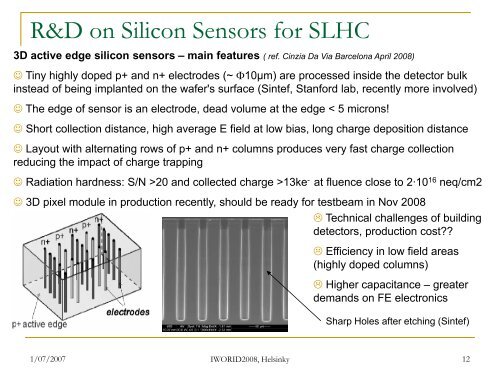
R&D on Silicon Sensors for SLHC<br />
3D active edge silicon sensors – main features ( ref. Cinzia Da Via Barcelona April 2008)<br />
☺ Tiny highly doped p+ and n+ electrodes (~ Φ10μm) are processed inside the detector bulk<br />
instead <strong>of</strong> being implanted on the wafer's surface (Sintef, Stanford lab, recently more involved)<br />
☺ The edge <strong>of</strong> sensor is an electrode, dead volume at the edge < 5 microns!<br />
☺ Short collection distance, high average E field at low bias, long charge deposition distance<br />
☺ Layout with alternating rows <strong>of</strong> p+ and n+ columns produces very fast charge collection<br />
reducing the impact <strong>of</strong> charge trapping<br />
☺ Radiation hardness: S/N >20 and collected charge >13ke - at fluence close to 2·10 16 neq/cm2<br />
☺ 3D pixel module in production recently, should be ready for testbeam in Nov 2008<br />
Technical challenges <strong>of</strong> building<br />
detectors, production cost??<br />
Efficiency in low field areas<br />
(highly doped columns)<br />
Higher capacitance – greater<br />
demands on FE electronics<br />
Sharp Holes after etching (Sintef)<br />
1/07/2007 IWORID2008, Helsinky 12