Petr SICHO - Helsinki Institute of Physics
Petr SICHO - Helsinki Institute of Physics
Petr SICHO - Helsinki Institute of Physics

Create successful ePaper yourself
Turn your PDF publications into a flip-book with our unique Google optimized e-Paper software.
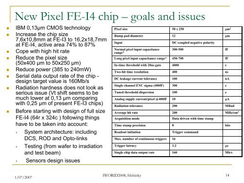
New Pixel FE-I4 chip – goals and issues<br />
• IBM 0,13μm CMOS technology<br />
• Increase the chip size<br />
7,6x10,8mm at FE-I3 to 16,2x18,7mm<br />
at FE-I4, active area 74% to 87%<br />
• Cope with high hit rate<br />
• Reduce the pixel size<br />
(50x400 μm to 50x250 μm)<br />
• Reduce power (385 to 240mW)<br />
• Serial data output rate <strong>of</strong> the chip -<br />
design target value is 160Mb/s<br />
• Radiation hardness does not look as<br />
serious issue (Vt shift seems to be<br />
much lower at 0,13 μm comparing<br />
with 0,25 μm <strong>of</strong> present FE-I3 chips)<br />
• Before starting with design <strong>of</strong> full size<br />
FE-I4 (64r x 324c ) following things<br />
have to be taken into account:<br />
• System architecture: including<br />
DCS, ROD and Opto-links<br />
• Testing (from wafer to irradiation<br />
and test beam)<br />
• Sensors design issues<br />
Pixel size 50 x 250 μm 2<br />
Bump pad diameter 12 μm<br />
Input<br />
Normal pixel input capacitance<br />
range*<br />
DC-coupled negative polarity<br />
300-500 fF<br />
Long pixel input capacitance range* 450-700 fF<br />
In-time threshold with 20ns gate 4000 e<br />
Two-hit time resolution 400 ns<br />
DC leakage current tolerance 100 nA<br />
Single channel ENC sigma (400fF) 300 e<br />
Tuned threshold dispersion 100 e<br />
Analog supply current/pixel @400fF 10 μA<br />
Radiation tolerance 200 MRad<br />
Average hit rate 200 MHz/cm 2<br />
Acquisition mode<br />
Data driven with time stamp<br />
Time stamp precision 8 bits<br />
Readout initiation<br />
Max. number <strong>of</strong> continuous triggers 16<br />
Trigger command<br />
Trigger latency 3.2 μs<br />
Single chip data output rate 160 Mb/s<br />
1/07/2007<br />
IWORID2008, Helsinky 14