Petr SICHO - Helsinki Institute of Physics
Petr SICHO - Helsinki Institute of Physics
Petr SICHO - Helsinki Institute of Physics
You also want an ePaper? Increase the reach of your titles
YUMPU automatically turns print PDFs into web optimized ePapers that Google loves.
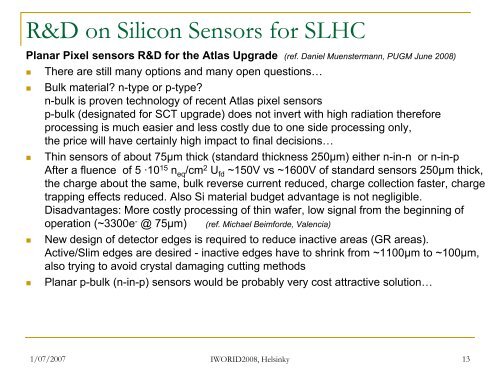
R&D on Silicon Sensors for SLHC<br />
Planar Pixel sensors R&D for the Atlas Upgrade (ref. Daniel Muenstermann, PUGM June 2008)<br />
• There are still many options and many open questions…<br />
• Bulk material? n-type or p-type?<br />
n-bulk is proven technology <strong>of</strong> recent Atlas pixel sensors<br />
p-bulk (designated for SCT upgrade) does not invert with high radiation therefore<br />
processing is much easier and less costly due to one side processing only,<br />
the price will have certainly high impact to final decisions…<br />
• Thin sensors <strong>of</strong> about 75μm thick (standard thickness 250μm) either n-in-n or n-in-p<br />
After a fluence <strong>of</strong> 5 ·10 15 n eq /cm 2 U fd ~150V vs ~1600V <strong>of</strong> standard sensors 250μm thick,<br />
the charge about the same, bulk reverse current reduced, charge collection faster, charge<br />
trapping effects reduced. Also Si material budget advantage is not negligible.<br />
Disadvantages: More costly processing <strong>of</strong> thin wafer, low signal from the beginning <strong>of</strong><br />
operation (~3300e - @ 75μm) (ref. Michael Beimforde, Valencia)<br />
• New design <strong>of</strong> detector edges is required to reduce inactive areas (GR areas).<br />
Active/Slim edges are desired - inactive edges have to shrink from ~1100μm to ~100μm,<br />
also trying to avoid crystal damaging cutting methods<br />
• Planar p-bulk (n-in-p) sensors would be probably very cost attractive solution…<br />
1/07/2007 IWORID2008, Helsinky 13


