Xilinx UG393 Spartan-6 FPGA PCB Design Guide
Xilinx UG393 Spartan-6 FPGA PCB Design Guide
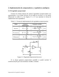
Xilinx UG393 Spartan-6 FPGA PCB Design Guide

You also want an ePaper? Increase the reach of your titles
YUMPU automatically turns print PDFs into web optimized ePapers that Google loves.
Chapter 2: Power Distribution System<br />
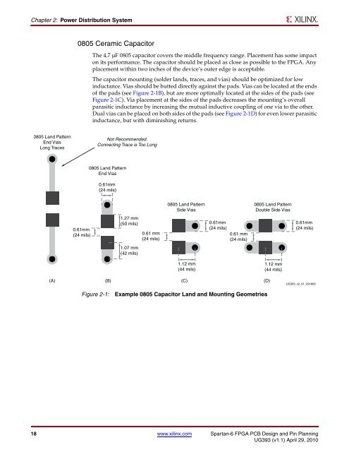
0805 Ceramic Capacitor<br />
The 4.7 µF 0805 capacitor covers the middle frequency range. Placement has some impact<br />
on its performance. The capacitor should be placed as close as possible to the <strong>FPGA</strong>. Any<br />
placement within two inches of the device’s outer edge is acceptable.<br />
The capacitor mounting (solder lands, traces, and vias) should be optimized for low<br />
inductance. Vias should be butted directly against the pads. Vias can be located at the ends<br />
of the pads (see Figure 2-1B), but are more optimally located at the sides of the pads (see<br />
Figure 2-1C). Via placement at the sides of the pads decreases the mounting’s overall<br />
parasitic inductance by increasing the mutual inductive coupling of one via to the other.<br />
Dual vias can be placed on both sides of the pads (see Figure 2-1D) for even lower parasitic<br />
inductance, but with diminishing returns.<br />
X-Ref Target - Figure 2-1<br />
0805 Land Pattern<br />
End Vias<br />
Long Traces<br />
Not Recommended.<br />
Connecting Trace is Too Long<br />
0805 Land Pattern<br />
End Vias<br />
0.61mm<br />
(24 mils)<br />
0805 Land Pattern<br />
Side Vias<br />
0805 Land Pattern<br />
Double Side Vias<br />
0.61mm<br />
(24 mils)<br />
1.27 mm<br />
(50 mils)<br />
0.61 mm<br />
(24 mils)<br />
0.61mm<br />
(24 mils)<br />
0.61 mm<br />
(24 mils)<br />
0.61mm<br />
(24 mils)<br />
1.07 mm<br />
(42 mils)<br />
1.12 mm<br />
(44 mils)<br />
1.12 mm<br />
(44 mils)<br />
(A)<br />
(B)<br />
(C)<br />
(D)<br />
<strong>UG393</strong>_c2_01_091809<br />
Figure 2-1:<br />
Example 0805 Capacitor Land and Mounting Geometries<br />
18 www.xilinx.com <strong>Spartan</strong>-6 <strong>FPGA</strong> <strong>PCB</strong> <strong>Design</strong> and Pin Planning<br />
<strong>UG393</strong> (v1.1) April 29, 2010