Xilinx UG393 Spartan-6 FPGA PCB Design Guide
Xilinx UG393 Spartan-6 FPGA PCB Design Guide
Xilinx UG393 Spartan-6 FPGA PCB Design Guide

You also want an ePaper? Increase the reach of your titles
YUMPU automatically turns print PDFs into web optimized ePapers that Google loves.
Chapter 5: <strong>Design</strong> of Transitions for High-Speed Signals<br />
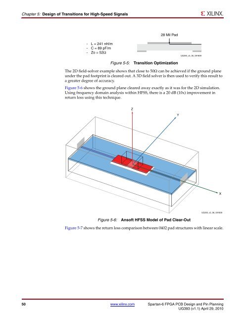
X-Ref Target - Figure 5-5<br />
28 Mil Pad<br />
- L = 241 nH/m<br />
- C = 89 pF/m<br />
- Zo = 52Ω<br />
<strong>UG393</strong>_c5_05_091809<br />
Figure 5-5:<br />
Transition Optimization<br />
The 2D field-solver example shows that close to 50Ω can be achieved if the ground plane<br />
under the pad footprint is cleared out. A 3D field solver is then used to verify this result to<br />
a greater degree of accuracy.<br />
Figure 5-6 shows the ground plane cleared away exactly as it was for the 2D simulation.<br />
Using frequency domain analysis within HFSS, there is a 20 dB (10x) improvement in<br />
return loss using this technique.<br />
X-Ref Target - Figure 5-6<br />
Z<br />
Y<br />
X<br />
<strong>UG393</strong>_c5_06_091809<br />
Figure 5-6:<br />
Ansoft HFSS Model of Pad Clear-Out<br />
Figure 5-7 shows the return loss comparison between 0402 pad structures with linear scale.<br />
50 www.xilinx.com <strong>Spartan</strong>-6 <strong>FPGA</strong> <strong>PCB</strong> <strong>Design</strong> and Pin Planning<br />
<strong>UG393</strong> (v1.1) April 29, 2010